


-
高能透射电子束照射下聚合物薄膜的带电效应严重影响其电子显微学检测的可靠性. 采用数值计算方法研究了聚合物薄膜的带电效应. 基于Monte Carlo方法模拟了电子的散射过程, 采用有限差分法处理电荷的输运、俘获和复合过程, 获得了净电荷、内建电场、表面出射电流、透射电流等动态分布特性, 分析了薄膜厚度、电子束能量对相关带电特性的影响. 结果表明: 由于近表面电子的出射, 样品内部净电荷、空间电位沿入射方向均呈现先为正、后为负的分布特性, 导致部分出射电子返回表面以及内部沉积电子向基底输运形成电子束感生电流; 随着电子束照射, 由于薄膜带电强度较弱, 透射电流随时间保持不变, 实际出射电流及样品电流分别下降和上升至一个稳定值. 薄膜厚度的增加使带电过程的瞬态时间增加, 引起表面电位下降以及实际出射电流、样品电流增大; 电子束能量的升高使透射电流增大, 样品电流减小, 引起表面正电位下降及实际出射电流的减小.The serious charging effect of polymer film with a thickness of the order of microns under the radiation of high-energy transmission electron beam, on the reliability of the micro-nano electronic device in electron microscopy detection is investigated. The charging effect of the polymer film is numerically calculated in this paper. The scattering process is simulated by the Monte Carlo method. The elastic scattering is calculated with the Rutherford scattering model. The inelastic scattering is simulated with the fast secondary electron (SE) model and the Penn model. The transport, the capture, and the recombination process of the charges are treated with the finite difference method. The fourth-order Runge-Kutta method is used to solve the trajectory of the emitted SEs. The dynamic distributions of the net charge, the built-in electric field, the surface emission current, and the transmission current are investigated, and the influence of the film thickness and the beam energy on the charging characteristics are analyzed. The results show that due to the emission of electrons near the sample surface, the distribution of the net charge in the sample is first positive and then negative along the incident direction. In addition, under the irradiation,higher charge quantity is deposited in the sample, and the net charge density increases gradually. However, with long-time irradiation, the deposited electrons transport to the surface under the action of built-in electric field which reduces the surface net charge density. Therefore the net charge density tends to a stable value. The space potential is positive in the surface and negative inside the sample. Therefore some emitted SEs return to the surface, resulting in the electron beam-induced current. With the irradiation, the positive surface potential increases and tends to a stable value. Hence the actual surface emission current decreases to a stable value and the sample current increases to a stable value. The sample current remains unchanged due to the weak charging strength. Increasing the film thickness leads the transient time to increase, which contributes to the decline of the surface potential and the increase of the actual emission currentand sample current. The increase of the beam energy causes the transmission current to increase and the sample current to decrease. In addition, it reduces the positive surface potential and the actual surface emission current accordingly. The results conduce to the decrease of the charging effect of the polymer film under the radiation of high-energy electron beam in the electron microscopy.
-
Keywords:
- charging effect /
- numerical simulation /
- transmission current /
- transport
[1] Zhang M, Wang X X, Cao W Q, Yuan J, Cao M S 2019 Adv. Optical Mater. 6 1900689
[2] Cao M S, Wang X X, Zhang M, Shu J C, Cao W Q, Yang H J, Fang X Y, Yuan J 2019 Adv. Funct. Mater. 29 1807398
 Google Scholar
[3] Reimer L 1993 Image Formation in Low Voltage Scanning Electron Microscopy (Bellingham: SPIE Optical Engineering Press) p71
[4] Fakhfakh S, Jbara O, Rondot S, Hadjadj A, Fakhfakh Z 2012 J. Non-Cryst. Solids 358 1157
Google Scholar
[5] Jbara O, Fakhfakh S, Belhaj M, Rondot S, Hadjadj A, Patat J M 2008 J. Phys. D 41 245504
Google Scholar
[6] Belhaj M, Paulmier T, Hanna R, Arnaout M, Balcon N, Payan D, Puech J 2014 Nucl. Instrum. Methods Phys. Rec., Sect. B 320 46
Google Scholar
[7] Paulmier T, Dirassen B, Payan D, Eesbeek M V 2009 IEEE Trans. Dielectr. Electr. Insul. 16 682
Google Scholar
[8] 黄建国, 韩建伟 2010 物理学报 59 2907
Google Scholar
Huang J G, Han J W 2010 Acta Phys. Sin. 59 2907
Google Scholar
[9] Ben Ammar L, Fakhfakh S, Jbara O, Rondot S 2017 J. Microsc. 265 322
Google Scholar
[10] Cazaux J 2010 J. Electron Spectrosc. Relat. Phenom. 176 58
Google Scholar
[11] Cornet N, Goeuriot D, Guerret-Piécourt C, Juvé D, Tréheux D, Touzin M, Fitting H J 2008 J. Appl. Phys. 103 064110
Google Scholar
[12] Rau E I, Fakhfakh S, Andrianov M V, Evstafeva E N, Jbara O, Rondot S, Mouze Z 2008 Nucl. Instrum. Methods Phys. Res. Sect. B 266 719
Google Scholar
[13] Cazaux J 2012 J. Electron Microsc. 61 261
Google Scholar
[14] Rau E I, Tatarintsev A A 2012 J. Surf. Invest. 6 911
Google Scholar
[15] Feng G B, Wang F, Hu T C, Cao M 2015 Chinese Phys. B 24 117901
Google Scholar
[16] Pan S M, Min D M, Wang X P, Hou X B, Wang L, Li S T 2019 IEEE Trans. Nucl. Sci. 66 549
Google Scholar
[17] Li W Q, Zhang H B 2010 Appl. Surf. Sci. 256 3482
Google Scholar
[18] Li W Q, Mu K, Xia R H 2011 Micron 42 443
Google Scholar
[19] 李维勤, 刘丁, 张海波 2014 物理学报 63 227303
Google Scholar
Li W Q, Liu D, Zhang H B 2014 Acta Phys. Sin. 63 227303
Google Scholar
[20] 李维勤, 郝杰, 张海波 2015 物理学报 64 086801
Google Scholar
Li W Q, Hao J, Zhang H B 2015 Acta Phys. Sin. 64 086801
Google Scholar
[21] Saloum S, Akel M, Alkhaled B 2009 J. Phys. D 42 085201
Google Scholar
[22] Barman P, Singh M S, Maibam J, Brojen R K, Sharma B I 2010 Ind. J. Phys. 84 711
Google Scholar
[23] 翁明, 胡天存, 曹猛, 徐伟军 2015 物理学报 64 157901
Google Scholar
Weng M, Hu T C, Cao M, Xu W J 2015 Acta Phys. Sin. 64 157901
Google Scholar
[24] 封国宝, 曹猛, 崔万照, 李军, 刘纯亮, 王芳 2017 物理学报 66 067901
Google Scholar
Feng G B, Cao M, Cui W Z, Li J, Liu C L, Wang F 2017 Acta Phys. Sin. 66 067901
Google Scholar
[25] Joy D C 1995 Monte Carlo Modeling for Electron Microscopy and Microanalysis (New York: Oxford University Press) p27
[26] You D S, Li H M, Ding Z J 2018 J. Electron Spectrosc. Relat. Phenom. 222 156
Google Scholar
[27] Da B, Mao S F, Zhang G H, Ding Z J 2012 J. Appl. Phys. 112 034310
Google Scholar
[28] Touzin M, Goeuriot D, Guerret-Piécourt C, Juvé D, Tréheux D, Fitting H J 2006 J. Appl. Phys. 99 114110
Google Scholar
[29] Cao M S, Shu J C, Wang X X, Wang X, Zhang M, Yang H J, Fang X, Yuan J 2019 Annalen Der Physik 531 1800390
Google Scholar
[30] Fang X Y, Yu X X, Zheng H M, Jin H B, Wang L, Cao M S 2015 Phys. Lett. A 379 2245
Google Scholar
[31] Li S L, Yu X X, Li Y L, Jia Y H, Fang X Y, Cao M S 2019 Eur. Phys. J. B 92 155
Google Scholar
[32] Song Z G, Ong C K, Gong H 1997 Appl. Surf. Sci. 119 169
Google Scholar
[33] Sessler G M 1992 IEEE T. Electr. Insul. 27 961
Google Scholar
[34] Sessler G M, Figueiredo M T, Ferreria G F L 2004 IEEE T. Dielect. El. Inl. 11 192
[35] Li Y J, Li S L, Gong P, Li Y L, Fang X Y, Jia Y H, Cao M S 2018 Physica E 104 247
Google Scholar
[36] Rau E I 2008 Appl. Surf. Sci. 254 2110
Google Scholar
-
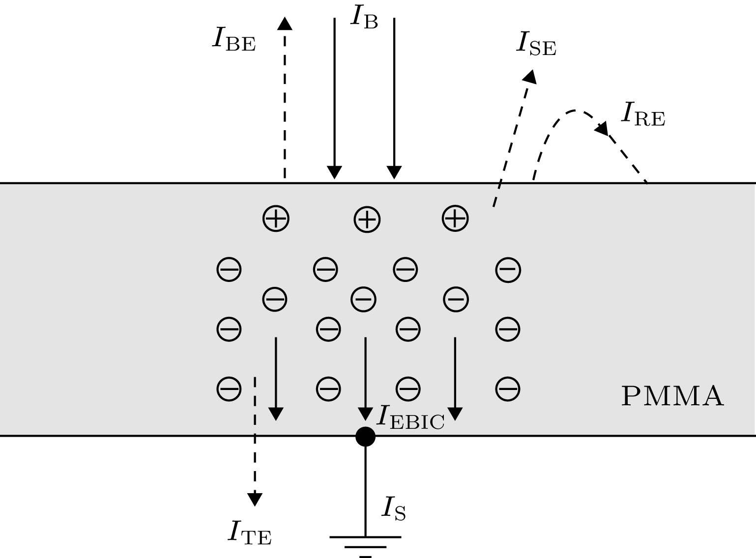
图 1 高能电子与PMMA薄膜相互作用示意图
Fig. 1. Interaction between high-energy electrons and PMMA thin film.
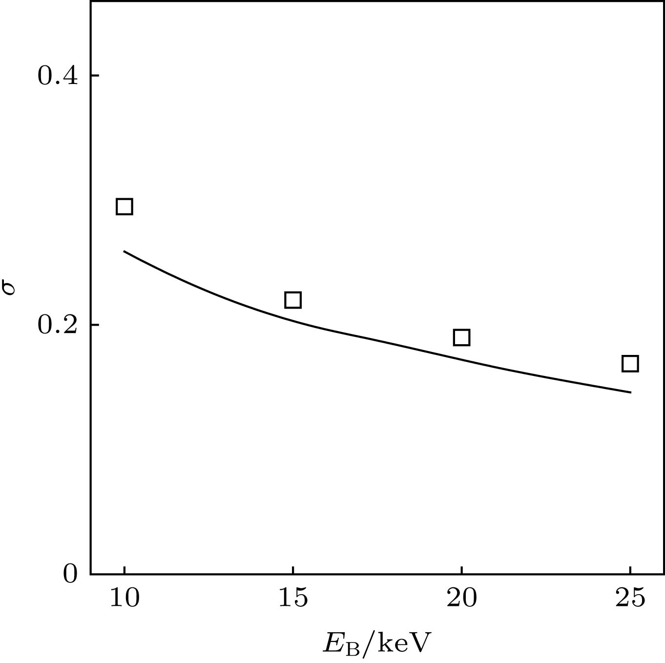
图 3 电子总产额的模拟(线条)和测量(方块)结果
Fig. 3. Simulated (lines) and experimental (squares) electron total yields.
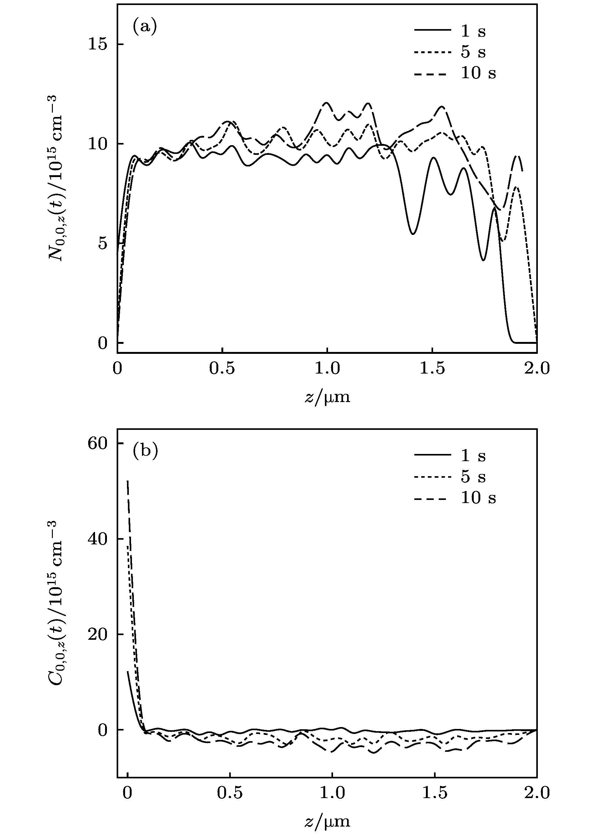
图 4 样品内部入射方向电荷分布 (a) 电子密度; (b) 净电荷密度
Fig. 4. Charges distribution along the incident direction: (a) Electron density ; (b) net charge density.
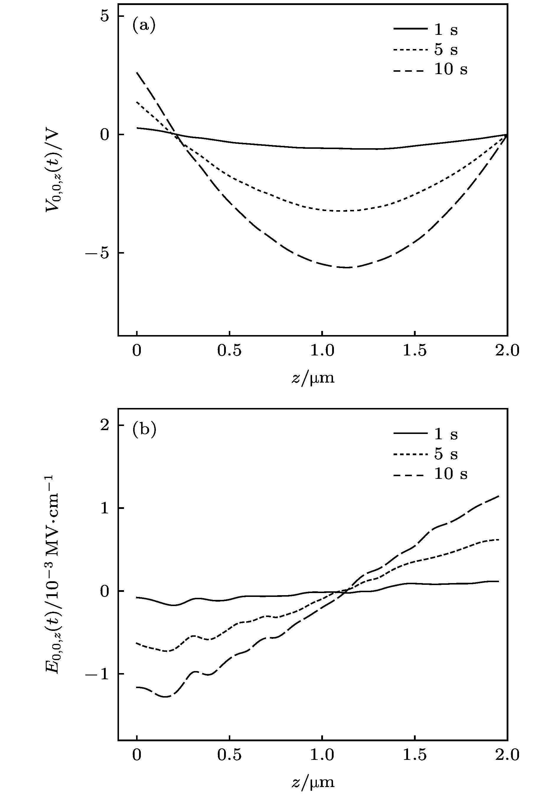
图 5 (a) 空间电位; (b) 电场强度沿入射方向分布
Fig. 5. (a) Space potential and (b) electric field along the incident direction.

图 6 表面电位VS和出射电子电流Iσ时变特性
Fig. 6. The surface potential VS and emission current Iσ as function of time.

图 7 透射电流ITE和样品电流IS时变特性
Fig. 7. The transmission current ITE and the sample current IS as function of time.
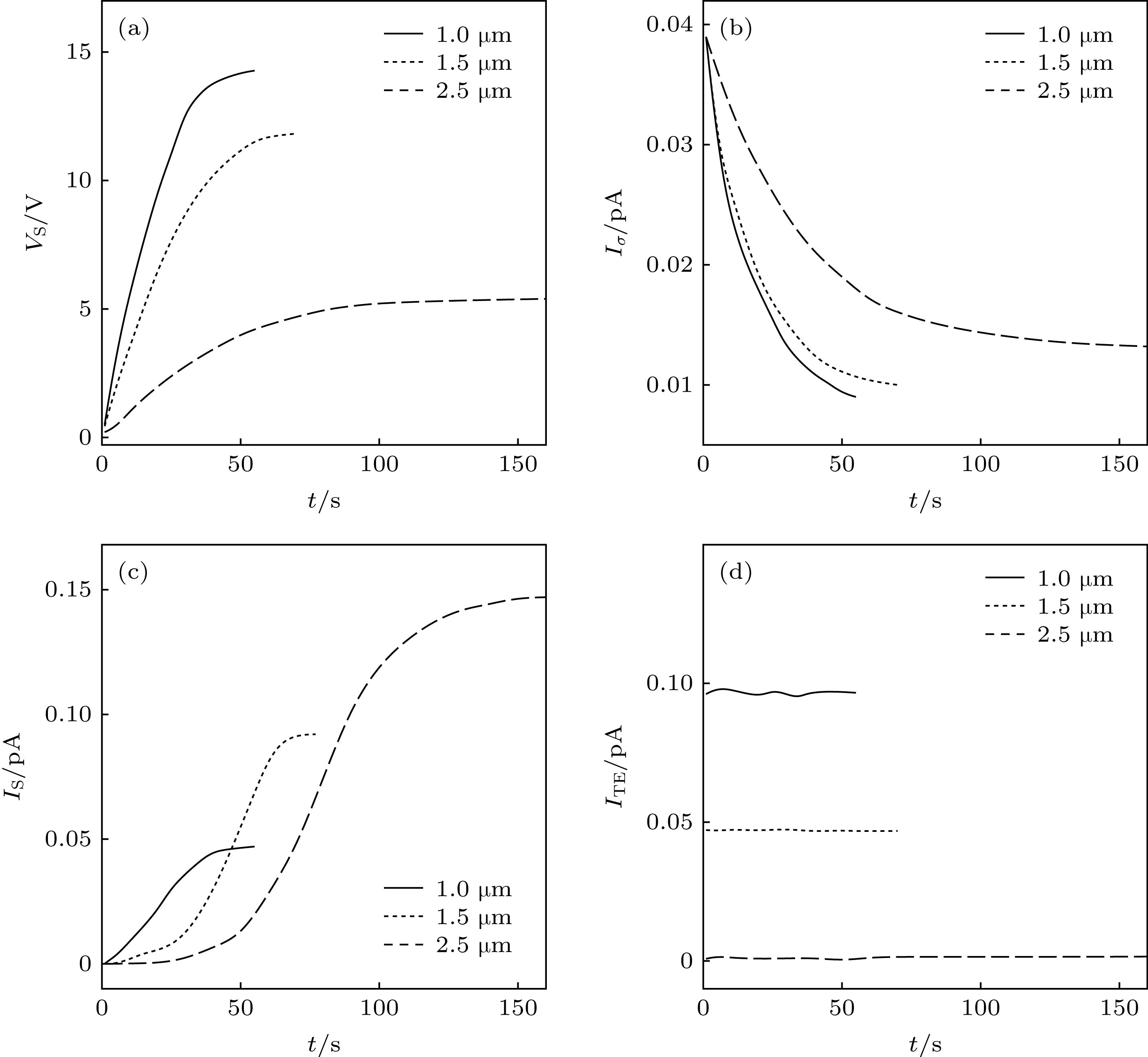
图 8 不同厚度下的带电特性 (a) 表面电位; (b) 表面出射电流; (c) 样品电流; (d) 透射电流
Fig. 8. Charging characteristics under different thicknesses: (a) Surface potential; (b) surface emission current; (c) sample current; (d) transmission current.

图 9 不同入射能量下带电特性 (a) 表面电位; (b) 表面出射电流; (c) 样品电流; (d) 透射电流
Fig. 9. Charging characteristics under different beam energies: (a) Surface potential; (b) surface emission current; (c) sample current; (d) transmission current.
表 1 参数默认取值
Table 1. Default values of parameters.
参数 取值 单位 电子束能量EB 10 keV 束流 0.16 pA 样品厚度H 2 μm 复合率 10–14 cm–3·s–1 电子迁移率μ 10–10 cm2·V–1·s–1 陷阱体密度Ntrap 1017 cm–3  下载: 导出CSV
-
[1] Zhang M, Wang X X, Cao W Q, Yuan J, Cao M S 2019 Adv. Optical Mater. 6 1900689
[2] Cao M S, Wang X X, Zhang M, Shu J C, Cao W Q, Yang H J, Fang X Y, Yuan J 2019 Adv. Funct. Mater. 29 1807398
Google Scholar
[3] Reimer L 1993 Image Formation in Low Voltage Scanning Electron Microscopy (Bellingham: SPIE Optical Engineering Press) p71
[4] Fakhfakh S, Jbara O, Rondot S, Hadjadj A, Fakhfakh Z 2012 J. Non-Cryst. Solids 358 1157
Google Scholar
[5] Jbara O, Fakhfakh S, Belhaj M, Rondot S, Hadjadj A, Patat J M 2008 J. Phys. D 41 245504
Google Scholar
[6] Belhaj M, Paulmier T, Hanna R, Arnaout M, Balcon N, Payan D, Puech J 2014 Nucl. Instrum. Methods Phys. Rec., Sect. B 320 46
Google Scholar
[7] Paulmier T, Dirassen B, Payan D, Eesbeek M V 2009 IEEE Trans. Dielectr. Electr. Insul. 16 682
Google Scholar
[8] 黄建国, 韩建伟 2010 物理学报 59 2907
Google Scholar
Huang J G, Han J W 2010 Acta Phys. Sin. 59 2907
Google Scholar
[9] Ben Ammar L, Fakhfakh S, Jbara O, Rondot S 2017 J. Microsc. 265 322
Google Scholar
[10] Cazaux J 2010 J. Electron Spectrosc. Relat. Phenom. 176 58
Google Scholar
[11] Cornet N, Goeuriot D, Guerret-Piécourt C, Juvé D, Tréheux D, Touzin M, Fitting H J 2008 J. Appl. Phys. 103 064110
Google Scholar
[12] Rau E I, Fakhfakh S, Andrianov M V, Evstafeva E N, Jbara O, Rondot S, Mouze Z 2008 Nucl. Instrum. Methods Phys. Res. Sect. B 266 719
Google Scholar
[13] Cazaux J 2012 J. Electron Microsc. 61 261
Google Scholar
[14] Rau E I, Tatarintsev A A 2012 J. Surf. Invest. 6 911
Google Scholar
[15] Feng G B, Wang F, Hu T C, Cao M 2015 Chinese Phys. B 24 117901
Google Scholar
[16] Pan S M, Min D M, Wang X P, Hou X B, Wang L, Li S T 2019 IEEE Trans. Nucl. Sci. 66 549
Google Scholar
[17] Li W Q, Zhang H B 2010 Appl. Surf. Sci. 256 3482
Google Scholar
[18] Li W Q, Mu K, Xia R H 2011 Micron 42 443
Google Scholar
[19] 李维勤, 刘丁, 张海波 2014 物理学报 63 227303
Google Scholar
Li W Q, Liu D, Zhang H B 2014 Acta Phys. Sin. 63 227303
Google Scholar
[20] 李维勤, 郝杰, 张海波 2015 物理学报 64 086801
Google Scholar
Li W Q, Hao J, Zhang H B 2015 Acta Phys. Sin. 64 086801
Google Scholar
[21] Saloum S, Akel M, Alkhaled B 2009 J. Phys. D 42 085201
Google Scholar
[22] Barman P, Singh M S, Maibam J, Brojen R K, Sharma B I 2010 Ind. J. Phys. 84 711
Google Scholar
[23] 翁明, 胡天存, 曹猛, 徐伟军 2015 物理学报 64 157901
Google Scholar
Weng M, Hu T C, Cao M, Xu W J 2015 Acta Phys. Sin. 64 157901
Google Scholar
[24] 封国宝, 曹猛, 崔万照, 李军, 刘纯亮, 王芳 2017 物理学报 66 067901
Google Scholar
Feng G B, Cao M, Cui W Z, Li J, Liu C L, Wang F 2017 Acta Phys. Sin. 66 067901
Google Scholar
[25] Joy D C 1995 Monte Carlo Modeling for Electron Microscopy and Microanalysis (New York: Oxford University Press) p27
[26] You D S, Li H M, Ding Z J 2018 J. Electron Spectrosc. Relat. Phenom. 222 156
Google Scholar
[27] Da B, Mao S F, Zhang G H, Ding Z J 2012 J. Appl. Phys. 112 034310
Google Scholar
[28] Touzin M, Goeuriot D, Guerret-Piécourt C, Juvé D, Tréheux D, Fitting H J 2006 J. Appl. Phys. 99 114110
Google Scholar
[29] Cao M S, Shu J C, Wang X X, Wang X, Zhang M, Yang H J, Fang X, Yuan J 2019 Annalen Der Physik 531 1800390
Google Scholar
[30] Fang X Y, Yu X X, Zheng H M, Jin H B, Wang L, Cao M S 2015 Phys. Lett. A 379 2245
Google Scholar
[31] Li S L, Yu X X, Li Y L, Jia Y H, Fang X Y, Cao M S 2019 Eur. Phys. J. B 92 155
Google Scholar
[32] Song Z G, Ong C K, Gong H 1997 Appl. Surf. Sci. 119 169
Google Scholar
[33] Sessler G M 1992 IEEE T. Electr. Insul. 27 961
Google Scholar
[34] Sessler G M, Figueiredo M T, Ferreria G F L 2004 IEEE T. Dielect. El. Inl. 11 192
[35] Li Y J, Li S L, Gong P, Li Y L, Fang X Y, Jia Y H, Cao M S 2018 Physica E 104 247
Google Scholar
[36] Rau E I 2008 Appl. Surf. Sci. 254 2110
Google Scholar

 下载:
下载:
计量
- 文章访问数: 9368
- PDF下载量: 71
- 被引次数: 0
