


-
为了研究热阴极表面形貌对电子发射能力的影响, 使用飞秒激光微纳加工技术在光滑的热阴极表面制备不同尺寸和形状的周期性条纹结构, 并使用相同的制备工艺对阴极进行除气和激活. 测试结果显示: 阴极表面周期性条纹结构可有效增强阴极的电子发射能力, 正交双向条纹结构表面阴极的发射电流密度高于单向条纹结构表面阴极的发射电流密度, 而且随条纹结构尺寸的降低, 阴极的电子发射能力逐渐增强. 对阴极表面形貌进行仿真, 发现微尖顶端位置在强电场的作用下具有较强的电子发射能力. 当阴极表面微尖底部直径与高度比值(r/h)较小时, 微尖的侧面仍是阴极电子发射的主要区域, 但是随着r/h减小, 阴极的电子发射区域逐渐由微尖侧面发射向微尖顶端转移, 场助电子发射效应成为阴极电子发射的主要组成部分.As a kind of influence factor, the surface topography determines the uniformity and current of peritoneal impregnated diffusion cathode (M-type dispenser cathode) emitted electrons. It can be seen from the emission characteristics of the cathode in the micro-range that the lathe tool grains at the cathode surface can affect the current uniformity, and the electron emission will be enhanced. But the distribution of the lathe tool grains is uncontrollable. Therefore to fully utilize the promoting effect of surface stripes on electron emission, the effect of surface topography onthe emission property of M-type dispenser cathode is investigated. And the simplest way to change the surface morphology of cathode surface is to fabricate a periodic stripe structure which can be divided into unidirectional stripe structure and orthogonal bidirectional stripe structure. And the orthogonal bidirectional stripe structure at the cathode surface can form micro-tip structure like the spindle cathode. To research the effect of surface topography on the emission properties of M-type dispenser cathode, the periodic stripe structures on the cathode surface with different sizes and shapes are processed by the femtosecond leaser in the fabrication of micro/nano-size microstructure. The cathodes are prepared with the same degassing and activated method. The test results of the cathodes show the periodic stripe structure on the cathode surface can effectively enhance the cathode electron emission capability. The emission current density of cathode with orthogonal bidirectional stripe is higher than that of cathode with unidirectional stripe. And with the stripe size declining, the emission capability is gradually enhanced. Also, this phenomenon occurs in the scandium-impregnated diffusion cathode. With the help of simulation of cathode surface topography, it is shown that the top of tip has a great electron emission capability for its strong electric field. When the ratio of bottom radius to height of the tip (r/h) is small, the side area is the main region of cathode electron emission. But as the r/h keeps decreasing, the main electron emission region is transferred from the side of tip to the top of tip, and the field assisted effect is the major component of the cathode electron emission.
-
Keywords:
- diffusion cathode /
- surface topography /
- current density /
- micro-tip array
[1] Chen D S, Lindau I, Hecht M H, Viescas A J, Nogami J, Spicer W E 1982 Appl. Surf. Sci. 13 321
 Google Scholar
[2] 廖复疆 2006 电子学报 34 513
Google Scholar
Liao F J 2006 Acta Electron. Sin. 34 513
Google Scholar
[3] 阴生毅, 张洪来, 杨靖鑫, 奎热西, 钱海杰, 王嘉欧, 王宇, 王欣欣 2011 电子与信息学报 33 3040
Yin S Y, Zhang H L, Yang J X, Urash I, Qian H J, Wang J O, Wang Y, Wang X X 2011 J. Electron. Inf. Technol. 33 3040
[4] Ares Fang C S, Maloney C E 1990 J. Vac. Sci. Technol. A 8 2329
Google Scholar
[5] Jones D, Mcneely D, Swanson L W 1979 Appl. Surf. Sci. 2 232
Google Scholar
[6] 任峰, 阴生毅, 卢志鹏, 李阳, 王宇, 张申金, 杨峰, 卫东 2017 物理学报 66 187901
Google Scholar
Ren F, Yin S Y, Lu Z P, Li Y, Wang Y, Zhang S J, Yang F, Wei D 2017 Acta Phys. Sin. 66 187901
Google Scholar
[7] Barik R, Bera A, Tanwar A K, Baek I K, Eom K, Sattorov M A, Min S H, Kwon O J, Park G S 2013 Int. J. Refract. Met. Hard Mat. 38 60
Google Scholar
[8] Brion D, Tonnerre J C, Shroff A M 1983 Appl. Surf. Sci. 16 55
Google Scholar
[9] 王光强, 王建国, 李小泽, 范如玉, 王行舟, 王雪锋, 童长江 2010 物理学报 59 8459
Google Scholar
Wang G Q, Wang J G, Li X Z, Fan R Y, Wang X Z, Wang X F, Tong C J 2010 Acta Phys. Sin. 59 8459
Google Scholar
[10] Booske J H, Dobbs R J, Joye C D, Kory C L, Neil G R, Park G, Park J, Temkin R J 2011 IEEE Trans. on Teraheeth Sci. Technol. 1 54
Google Scholar
[11] Wang Y, Wang J, Liu W, Zhang K, Li J 2007 IEEE Trans. Electron Dev. 54 1061
Google Scholar
[12] 梁文龙, 王亦曼, 刘伟, 李洪义, 王金淑 2014 物理学报 63 057901
Google Scholar
Liang W L, Wang Y M, Liu W, Li H Y, Wang J S 2014 Acta Phys. Sin. 63 057901
Google Scholar
[13] 李玉涛, 张洪来, 刘濮鲲, 张明晨 2006 物理学报 55 6677
Google Scholar
Li Y T, Zhang H L, Liu P K, Zhang M C 2006 Acta Phys. Sin. 55 6677
Google Scholar
[14] Gaertner G 2012 J. Vac. Sci. Technol. B 30 060801
Google Scholar
[15] Wang J, Liu W, Li L, Wang Y C, Wang Y, Zhou M 2009 IEEE Trans. Electron Dev. 56 779
Google Scholar
[16] Liu W, Wang Y, Wang J, Wang Y C 2011 IEEE Trans. Electron Dev. 58 1241
Google Scholar
[17] Meduri R, Shubankar S, Mukta J 2018 IEEE Trans. Electron Dev. 65 2083
Google Scholar
[18] Ryan J, Dane M, John B 2017 APL Mater. 5 116105
Google Scholar
[19] Bernard V, Wayne L O, Minchael C G, Charles O, Victor S, Allan V 2018 IEEE Trans. Electron Dev. 65 2077
Google Scholar
[20] Yang Y, Wang Y, Liu W, Pan Z, Li J, Wang J 2018 IEEE Trans. Electron Dev. 65 2072
Google Scholar
[21] Gartner G, Geittner P, Raasch D, Wiechert D U 1999 Appl. Surf. Sci. 146 22
Google Scholar
-
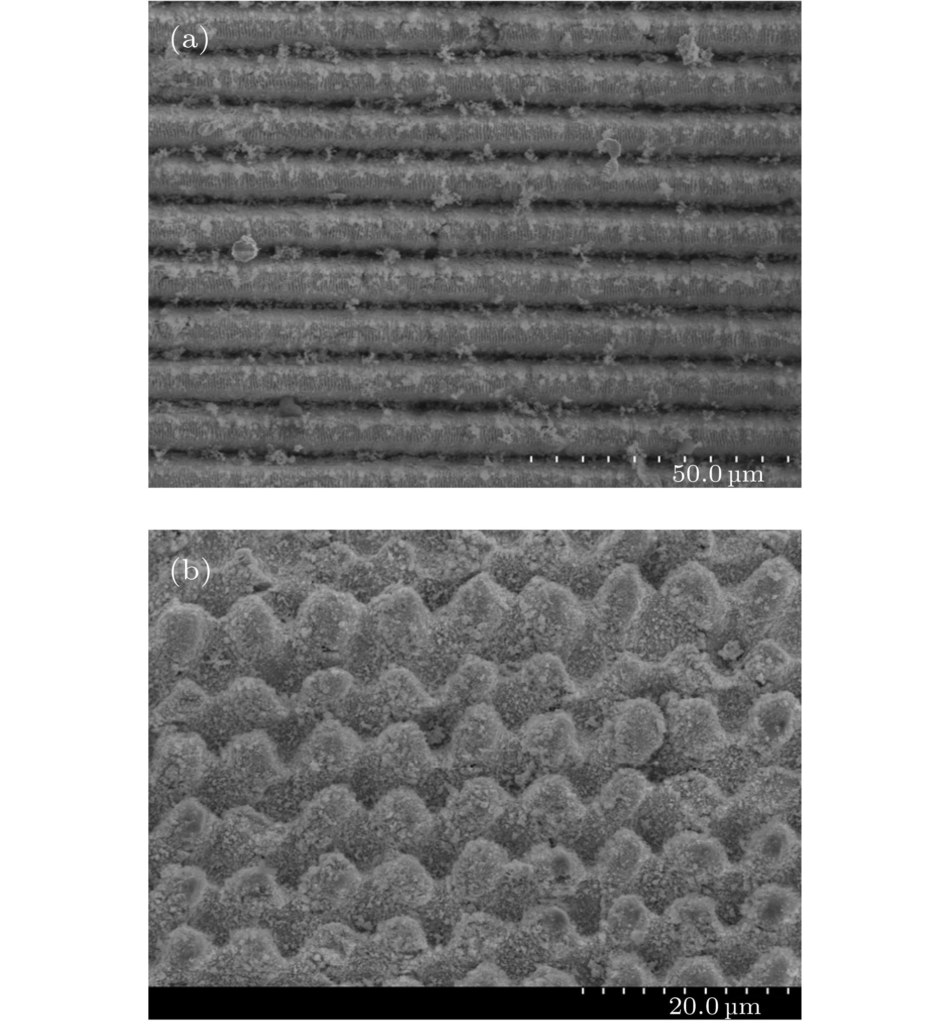
图 2 周期性条纹结构阴极的表面显微形貌 (a)单向条纹结构; (b)正交双向条纹结构
Fig. 2. Surface microtopography of cathode with periodic stripe structure: (a) Unidirectionalstripe structure; (b) orthogonal bidirectional stripe structure.

图 3 水冷真空二极管结构及阴极性能测试系统示意图(1为阴极, 2为玻壳, 3为阳极, 4为冷却水接口)
Fig. 3. Diagram of water-cooled vacuum diode and cathode performance testing system. Symbol 1, 2, 3 and 4 are cathode, glass shell, anode and cooling water connector, respectively.
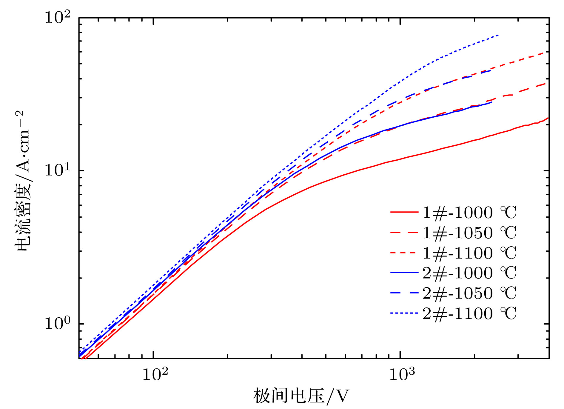
图 4 不同工作温度条件下阴极样品1和样品2发射电流密度特性
Fig. 4. Current density character of cathode sample 1 and 2 with different working temperature.

图 5 不同工作温度条件下阴极样品3和样品4的发射电流密度特性
Fig. 5. Current density character of cathode sample 3 and 4 with different working temperature.

图 6 极间距为0.1 mm时阴极样品4的发射电流密度特性
Fig. 6. Current density character of cathode sample 4 with polar distance 0.1 mm.

图 7 不同工作温度条件下阴极样品5和样品6发射电流密度特性
Fig. 7. Current density character of cathode sample 5 and 6 with different working temperature.
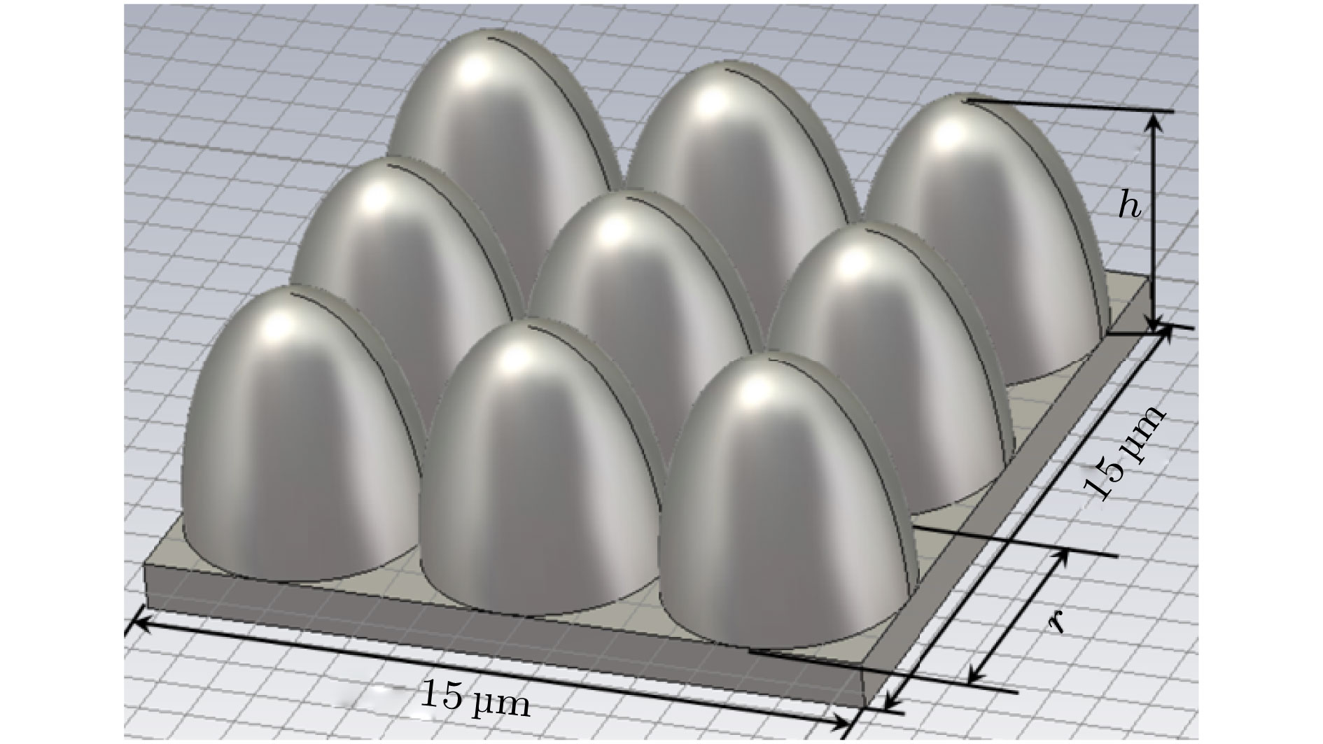
图 8 3 × 3阵列结构的阴极电子发射性能仿真模型
Fig. 8. Emulation model of electron emission performance of cathode with array 3 × 3.
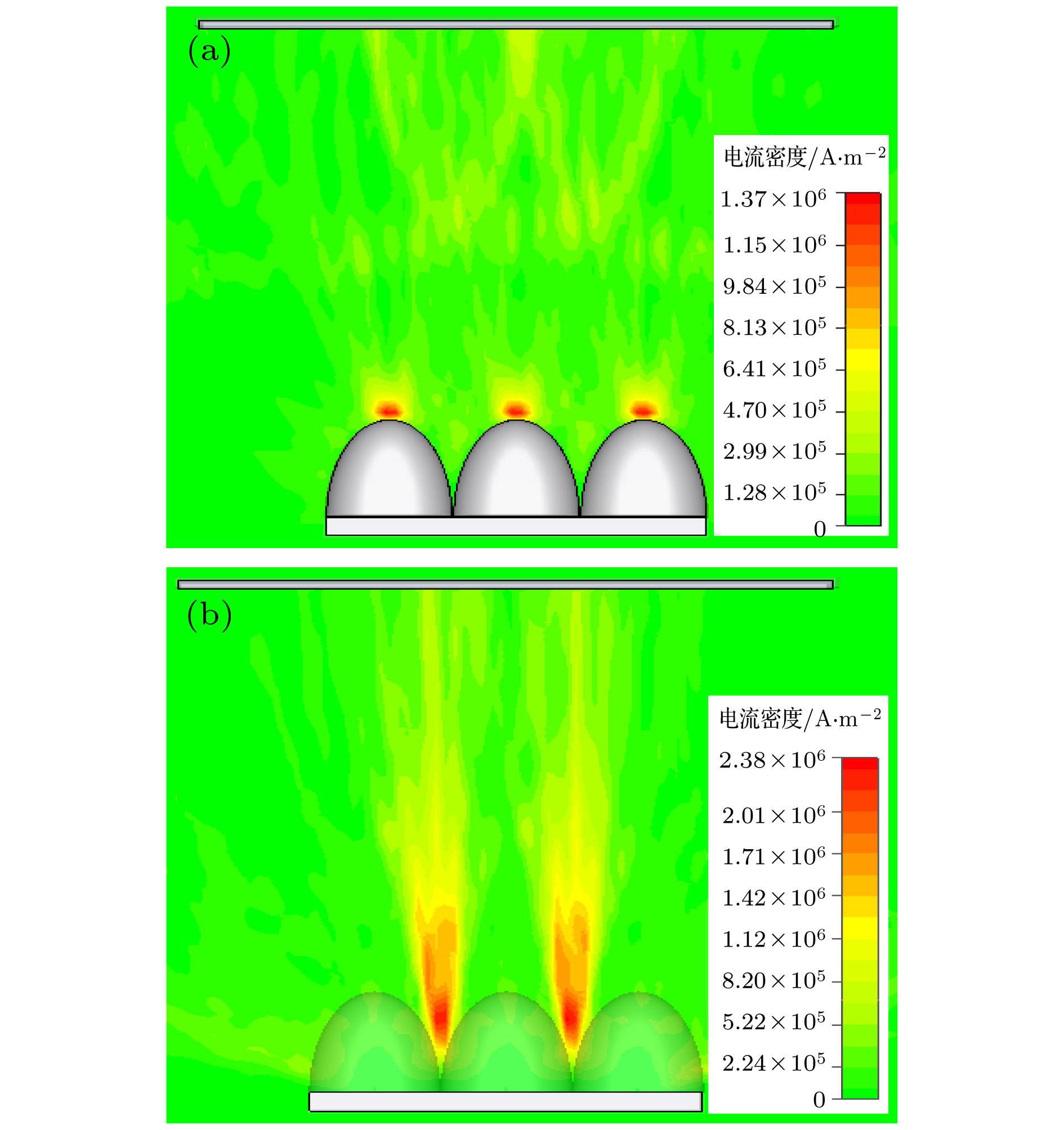
图 9 3 × 3阵列结构的阴极纵向截面处电子的空间分布 (a)微尖尖端位置截面; (b)微尖间隙位置截面
Fig. 9. Spatial distribution of electrons of longitudinal sections of cathode with array 3 × 3: (a) Cross section of top of tip; (b) cross section of clearance of tips.

图 10 距阴极表面微尖顶端
$10\;\text{μm}$ 位置处横向截面中的电子分布Fig. 10. Electronic distribution of lateral interface that far from the cathode surface about
$10\;\text{μm}.$ 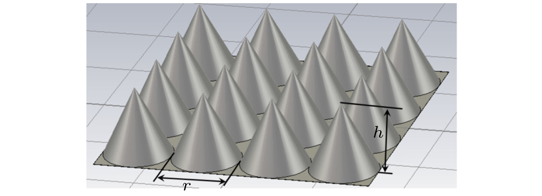
图 11 4 × 4阵列结构阴极表面理想结构模型
Fig. 11. Ideal structural model of cathode surface with array 4 × 4.

图 12 锥形微尖阵列结构中阴极电势分布
Fig. 12. Potential distribution of cathode at the tapered micro-tip array structure.
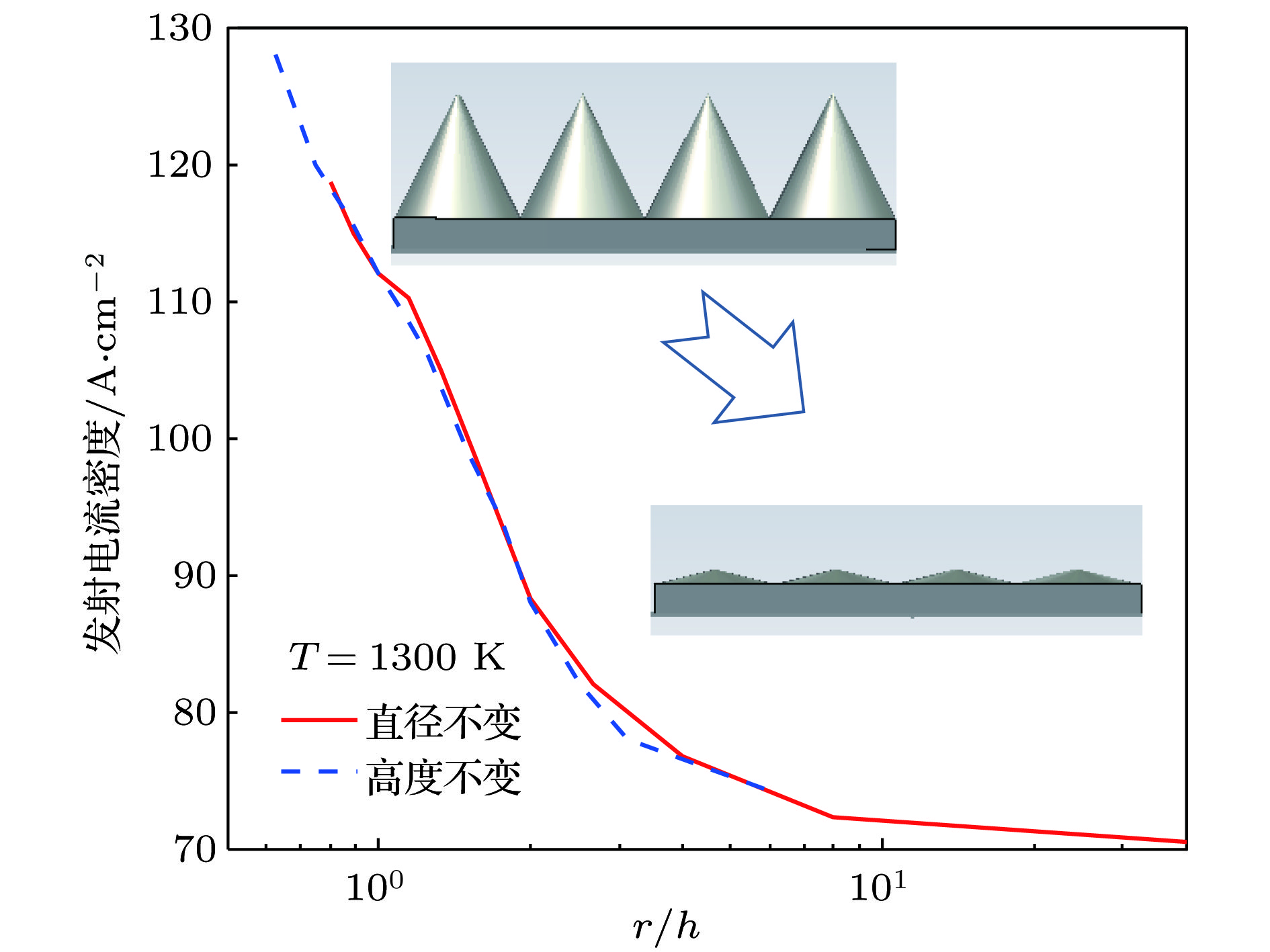
图 13 微尖结构r/h值对阴极发射电流密度的影响
Fig. 13. Effect of r/h value of micro-tip structure on emission current density of cathode.
表 1 阴极种类及其表面结构参数
Table 1. Type of cathode and surface structure parameters.
样品编号 阴极类型 条纹结构 条纹间距
$/\text{μm}$条纹深度
$/\text{μm}$1 覆膜浸渍
扩散阴极单向 50 50 2 覆膜浸渍
扩散阴极正交双向 50 50 3 覆膜浸渍
扩散阴极正交双向 35 35 4 覆膜浸渍
扩散阴极正交双向 8 8 5 钪酸盐
阴极单向 8 8 6 钪酸盐
阴极正交双向 8 8  下载: 导出CSV
表 2 阴极样品2、样品3和样品4的零场发射电流密度
Table 2. Zero field emission current density of cathode sample 2, 3 and 4.
测试温度/℃ 阴极样品2
/A·cm−2阴极样品3
/A·cm−2阴极样品4
/A·cm−21000 7.2 9.1 20.6 1050 12.3 17.8 35.5 1100 19.5 31.6 63.5
下载: 导出CSV
-
[1] Chen D S, Lindau I, Hecht M H, Viescas A J, Nogami J, Spicer W E 1982 Appl. Surf. Sci. 13 321
Google Scholar
[2] 廖复疆 2006 电子学报 34 513
Google Scholar
Liao F J 2006 Acta Electron. Sin. 34 513
Google Scholar
[3] 阴生毅, 张洪来, 杨靖鑫, 奎热西, 钱海杰, 王嘉欧, 王宇, 王欣欣 2011 电子与信息学报 33 3040
Yin S Y, Zhang H L, Yang J X, Urash I, Qian H J, Wang J O, Wang Y, Wang X X 2011 J. Electron. Inf. Technol. 33 3040
[4] Ares Fang C S, Maloney C E 1990 J. Vac. Sci. Technol. A 8 2329
Google Scholar
[5] Jones D, Mcneely D, Swanson L W 1979 Appl. Surf. Sci. 2 232
Google Scholar
[6] 任峰, 阴生毅, 卢志鹏, 李阳, 王宇, 张申金, 杨峰, 卫东 2017 物理学报 66 187901
Google Scholar
Ren F, Yin S Y, Lu Z P, Li Y, Wang Y, Zhang S J, Yang F, Wei D 2017 Acta Phys. Sin. 66 187901
Google Scholar
[7] Barik R, Bera A, Tanwar A K, Baek I K, Eom K, Sattorov M A, Min S H, Kwon O J, Park G S 2013 Int. J. Refract. Met. Hard Mat. 38 60
Google Scholar
[8] Brion D, Tonnerre J C, Shroff A M 1983 Appl. Surf. Sci. 16 55
Google Scholar
[9] 王光强, 王建国, 李小泽, 范如玉, 王行舟, 王雪锋, 童长江 2010 物理学报 59 8459
Google Scholar
Wang G Q, Wang J G, Li X Z, Fan R Y, Wang X Z, Wang X F, Tong C J 2010 Acta Phys. Sin. 59 8459
Google Scholar
[10] Booske J H, Dobbs R J, Joye C D, Kory C L, Neil G R, Park G, Park J, Temkin R J 2011 IEEE Trans. on Teraheeth Sci. Technol. 1 54
Google Scholar
[11] Wang Y, Wang J, Liu W, Zhang K, Li J 2007 IEEE Trans. Electron Dev. 54 1061
Google Scholar
[12] 梁文龙, 王亦曼, 刘伟, 李洪义, 王金淑 2014 物理学报 63 057901
Google Scholar
Liang W L, Wang Y M, Liu W, Li H Y, Wang J S 2014 Acta Phys. Sin. 63 057901
Google Scholar
[13] 李玉涛, 张洪来, 刘濮鲲, 张明晨 2006 物理学报 55 6677
Google Scholar
Li Y T, Zhang H L, Liu P K, Zhang M C 2006 Acta Phys. Sin. 55 6677
Google Scholar
[14] Gaertner G 2012 J. Vac. Sci. Technol. B 30 060801
Google Scholar
[15] Wang J, Liu W, Li L, Wang Y C, Wang Y, Zhou M 2009 IEEE Trans. Electron Dev. 56 779
Google Scholar
[16] Liu W, Wang Y, Wang J, Wang Y C 2011 IEEE Trans. Electron Dev. 58 1241
Google Scholar
[17] Meduri R, Shubankar S, Mukta J 2018 IEEE Trans. Electron Dev. 65 2083
Google Scholar
[18] Ryan J, Dane M, John B 2017 APL Mater. 5 116105
Google Scholar
[19] Bernard V, Wayne L O, Minchael C G, Charles O, Victor S, Allan V 2018 IEEE Trans. Electron Dev. 65 2077
Google Scholar
[20] Yang Y, Wang Y, Liu W, Pan Z, Li J, Wang J 2018 IEEE Trans. Electron Dev. 65 2072
Google Scholar
[21] Gartner G, Geittner P, Raasch D, Wiechert D U 1999 Appl. Surf. Sci. 146 22
Google Scholar


 下载:
下载:


计量
- 文章访问数: 13790
- PDF下载量: 107
- 被引次数: 0
