


-
In this study, the high-quality GaN films are prepared by a simple, green and low-cost plasma enhanced chemical vapor deposition (PECVD) method at 950 ℃, with Ga2O3 and N2 serving as a gallium source and a nitrogen source, respectively. In order to improve the crystal quality of GaN films and ascertain the photoresponse mechanism of GaN films, the effect of the preparation temperature of GaN buffer layer on the crystal quality and photoelectric properties of GaN thin films are investigated. It is indicated that with the increase of the buffer temperature of GaN films, the crystal quality of GaN films first increases and then decreases, and the highest crystal quality is obtained at 875 ℃. When buffer layer temperature is 875 ℃, the calculated total dislocation density is 9.74 × 109 cm–2, and the carrier mobility is 0.713 cm2·V–1·s–1. The crystal quality of GaN film after being annealed is improved. The total dislocation density of GaN film decreases to 7.38 × 109 cm–2, and the carrier mobility increases to 43.5 cm2·V–1·s–1. The UV-Vis absorption spectrum results indicate that the optical band gap of GaN film is 3.35 eV. The scanning electron microscope (SEM) results indicate that GaN film (buffer layer temperature is 875 ℃) has smooth surface and compact structure. The Hall and X-ray photoelectron spectroscopy (XPS) results indicate that there are N vacancies, Ga vacancies or O doping in the GaN film, which act as deep level to capture photogenerated electrons and holes. With the bias increasing, the photoresponsivity of the GaN film photodetector gradually increases and then reaches a saturation value. This is due to the deep levels produced by vacancy or O doping. In addition, photocurrent response and recovery of GaN film are slow, which is also due to the deep levels formed by vacancy or O doping. At 5-V bias, the photoresponsivity of GaN film is 0.2 A/W, rise time is 15.4 s, and fall time is 24 s. Therefore, the high-quality GaN film prepared by the proposed green and low-cost PECVD method present a strong potential application in ultraviolet photodetector. The PECVD method developed by us provides a feasible way of preparing high-quality GaN films, and the understanding of the photoresponse mechanism of GaN films provides a theoretical basis for the wide application of GaN films.
-
Keywords:
- GaN film /
- plasma chemical vapor deposition /
- crystal quality /
- photoresponsivity /
- photoresponse mechanism
[1] Liu L, Xia S, Diao Y, Lu F, Tian J 2020 Solid State Ionics 350 115327
 Google Scholar
[2] Wang X, Zhang Y, Chen X, He M, Liu C, Yin Y, Zou X, Li S 2014 Nanoscale 6 12009
Google Scholar
[3] Zhang X, Liu Q, Liu B, Yang W, Li J, Niu P, Jiang X 2017 J. Mater. Chem. C 5 4319
Google Scholar
[4] Peng M, Liu Y, Yu A, Zhang Y, Liu C, Liu J, Wu W, Zhang K, Shi X, Kou J, Zhai J, Wang Z L 2016 ACS Nano 10 1572
Google Scholar
[5] Chen X Y, Yip C T, Fung M K, Djurišić A B, Chan W K 2010 Appl. Phys. A 100 15
Google Scholar
[6] Li Y, Wang W, Li X, Huang L, Lin Z, Zheng Y, Chen X, Li G 2019 J. Alloys Compd. 771 1000
Google Scholar
[7] Deng G, Zhang Y, Yu Y, Yan L, Li P, Han X, Chen L, Zhao D, Du G 2018 Superlattice. Microstruct. 116 1
Google Scholar
[8] Liang Q, Wang R Z, Yang M Q, Ding Y, Wang C H 2020 Thin Solid Films 710 138266
Google Scholar
[9] Yang W J, Wang W L, Liu Z L, Li G Q 2015 Mater. Sci. Semicond. Process. 39 499
Google Scholar
[10] Okuno K, Oshio T, Shibata N, Honda Y, Yamaguchi M, Tanaka S, Amano H 2013 Phys. Status Solidi C 10 369
Google Scholar
[11] Bak S J, Mun D H, Jung K C, Park J H, Bae H J, Lee I W, Ha J S, Jeong T, Oh T S 2013 Electron. Mater. Lett. 9 367
Google Scholar
[12] Tran B T, Chang E Y, Lin K L, Luong T T, Yu H W, Huang M C, Chung C C, Trinh H D, Nguyen H Q, Nguyen C L, Luc Q H 2012 ECS Trans. 50 461
Google Scholar
[13] Huang W C, Chu C M, Wong Y Y, Chen K W, Lin Y K, Wu C H, Lee W I, Chang E Y 2016 Mater. Sci. Semicond. Process. 45 1
Google Scholar
[14] Zhao J W, Zhang Y F, Li Y H, Su C H, Song X M, Yan H, Wang R Z 2015 Sci. Rep. 5 17692
Google Scholar
[15] Ji Y H, Wang R Z, Feng X Y, Zhang Y F, Yan H 2017 J. Phys. Chem. C 121 24804
Google Scholar
[16] Feng X Y, Wang R Z, Liang Q, Ji Y H, Yang M Q 2019 Cryst. Growth. Des. 19 2687
Google Scholar
[17] 梁琦, 王如志, 杨孟骐, 王长昊, 刘金伟 2020 物理学报 69 087801
Google Scholar
Liang Q, Wang R Z, Yang M Q, Wang C H, Liu J W 2020 Acta Phys. Sin. 69 087801
Google Scholar
[18] Ramesh C, Tyagi P, Bhattacharyya B, Husale S, Maurya K K, Kumar M S, Kushvaha S S 2019 J. Alloys Compd. 770 572
Google Scholar
[19] Popovici G, Xu G Y, Botchkarev A, Kim W, Tang H, Salvador A, Morkoç H, Strange R, White J O 1997 J. Appl. Phys. 82 4020
Google Scholar
[20] Eckey L, Gfug U V, Holst J, Hoffmann A, Kaschner A, Siegle H, Thomsen C, Schineller B, Heime K, Heuken M, Schön O, Beccard R 1998 J. Appl. Phys. 84 5828
Google Scholar
[21] Greenlee J D, Feigelson B N, Anderson T J, Tadjer M J, Hite J K, Mastro M A, Eddy C R, Hobart K D, Kub F J 2014 J. Appl. Phys. 116 063502
Google Scholar
[22] Huang Y, Chen X D, Fung S, Beling C D, Ling C C, Wei Z F, Xu S J, Zhi C Y 2004 J. Appl. Phys. 96 1120
Google Scholar
[23] Hwang C Y, Schurman M J, Mayo W E 1997 J. Electron. Mater. 26 243
Google Scholar
[24] Jeong J K, Choi J H, Hwang C S, Kim H J, Lee J H, Lee J H, Kim C S 2004 Appl. Phys. Lett. 84 2575
Google Scholar
[25] Ng H M, Doppalapudi D, Moustakas T D, Weimann N G, Eastman L F 1998 Appl. Phys. Lett. 73 821
Google Scholar
[26] Lee J H, Hahm S H, Lee J H, Bae S B, Lee K S, Cho Y H, Lee J L 2003 Appl. Phys. Lett. 83 917
Google Scholar
[27] Wang Y Q, Wang R Z, Zhu M K, Wang B B, Wang B, Yan H 2013 Appl. Surf. Sci. 285 115
Google Scholar
[28] Lee C T, Lin Y J, Lin C H 2002 J. Appl. Phys. 92 3825
Google Scholar
[29] Gui Y, Yang L, Tian K, Zhang H, Fang S 2019 Sens. Actuators, B 288 104
Google Scholar
[30] Sun X, Li D, Jiang H, Li Z, Song H, Chen Y, Miao G 2011 Appl. Phys. Lett. 98 121117
Google Scholar
[31] Jhou Y D, Chang S J, Su Y K, Lee Y Y, Liu C H, Lee H C 2007 Appl. Phys. Lett. 91 103506
Google Scholar
[32] Golgir H R, Li D W, Keramatnejad K, Zou Q M, Xiao J, Wang F, Jiang L, Silvain J F, Lu Y F 2017 ACS Appl. Mater. Interfaces 9 21539
Google Scholar
[33] Müller A, Konstantinidis G, Androulidaki M, Dinescu A, Stefanescu A, Cismaru A, Neculoiu D, Pavelescu E, Stavrinidis A 2012 Thin Solid Films 520 2158
Google Scholar
[34] Xie F, Lu H, Xiu X, Chen D, Han P, Zhang R, Zheng Y 2011 Solid State Electron. 57 39
Google Scholar
[35] Osinsky A, Gangopadhyay S, Yang J W, Gaska R, Kuksenkov D, Temkin H, Shmagin I K, Chang Y C, Muth J F, Kolbas R M 1998 Appl. Phys. Lett. 72 551
Google Scholar
[36] Pant R, Shetty A, Chandan G, Roul B, Nanda K K, Krupanidhi S B 2018 ACS Appl. Mater. Interfaces 10 16918
Google Scholar
[37] Mukundan S, Mohan L, Chandan G, Roul B, Krupanidhi S B 2014 J. Appl. Phys. 116 204502
Google Scholar
-

图 1 不同制备温度缓冲层的未退火GaN薄膜的XRD图谱
Figure 1. The XRD pattern of unannealed GaN films with buffer layer fabricated at different temperature.

图 2 不同制备温度缓冲层的未退火GaN薄膜的XRC半高全宽曲线
Figure 2. The FWHM of XRCs of unannealed GaN films with buffer layer fabricated at different temperature.

图 3 不同制备温度缓冲层的未退火GaN薄膜的Raman光谱图
Figure 3. Raman spectra of unannealed GaN films with buffer layer fabricated at different temperature.
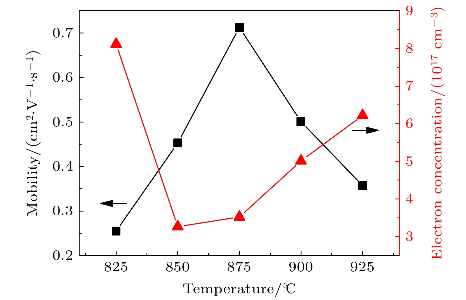
图 4 未退火GaN薄膜的缓冲层制备温度与电子浓度和迁移率的关系曲线
Figure 4. Electron concentration and mobility of unannealed GaN films with buffer layer at different temperature.
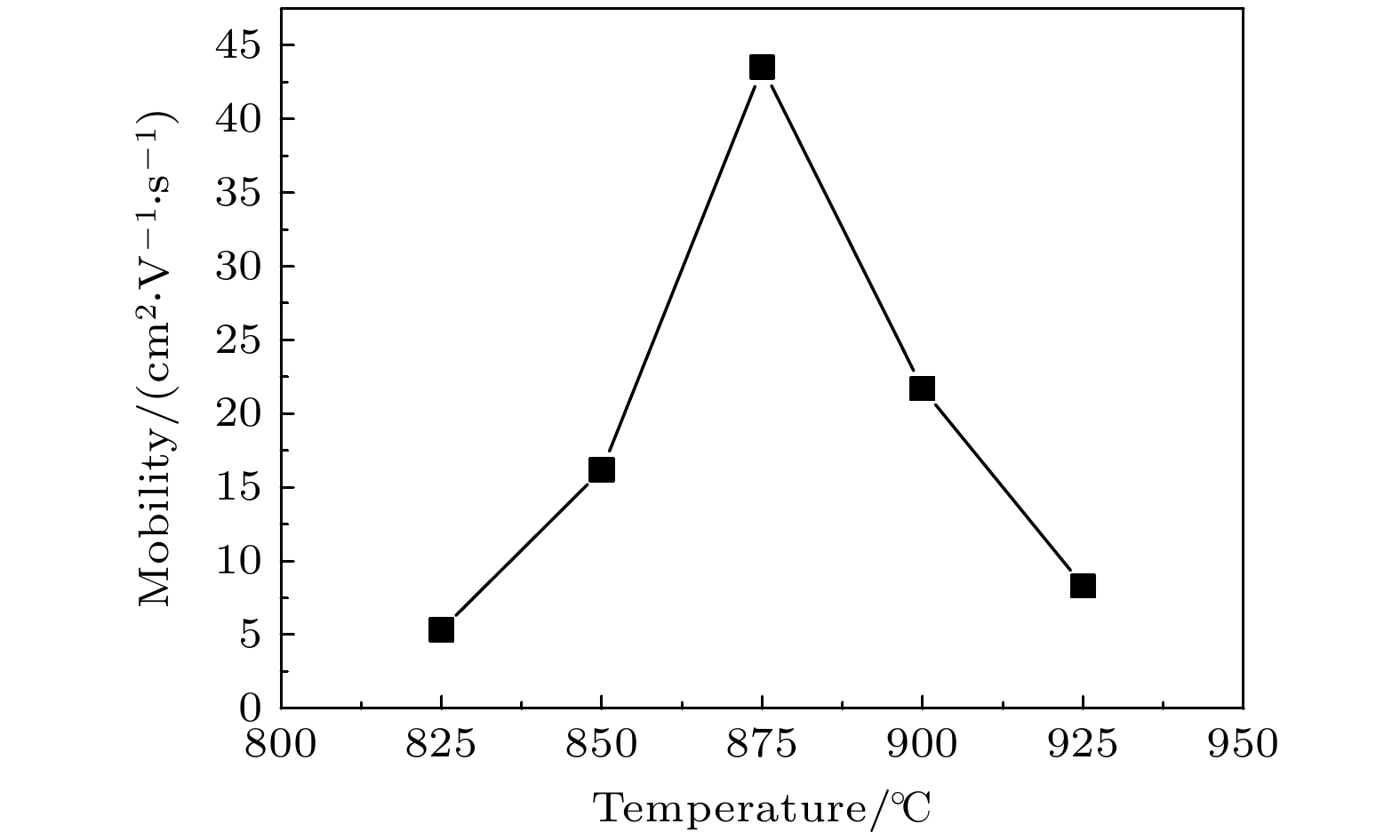
图 5 退火GaN薄膜的缓冲层制备温度与迁移率的关系曲线
Figure 5. Mobility of annealed GaN films with buffer layer at different temperature.

图 6 缓冲层制备温度为875 ℃的退火GaN薄膜的XRC图谱 (a) (100)面; (b) (101)面
Figure 6. The XRCs of annealed GaN fim with buffer layer at 875 ℃: (a) (100); (b) (101).
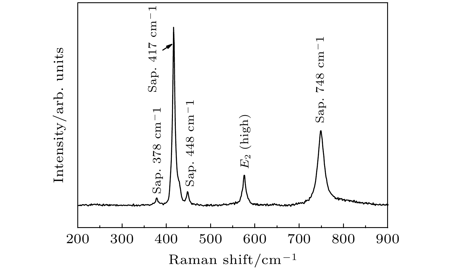
图 7 缓冲层制备温度为875 ℃的退火GaN薄膜的Raman光谱图
Figure 7. Raman spectra of annealed GaN fim with buffer layer at 875 ℃.

图 8 缓冲层制备温度为875 ℃的退火GaN薄膜的微观区域SEM图和实物图 (a)表面SEM图; (b)截面SEM图; (c) 退火GaN薄膜样品的实物图
Figure 8. SEM images and picture of annealed GaN film with buffer layer at 875 ℃: (a) SEM image of surface; (b) cross sectional SEM image; (c) the picture of annealed GaN film sample.
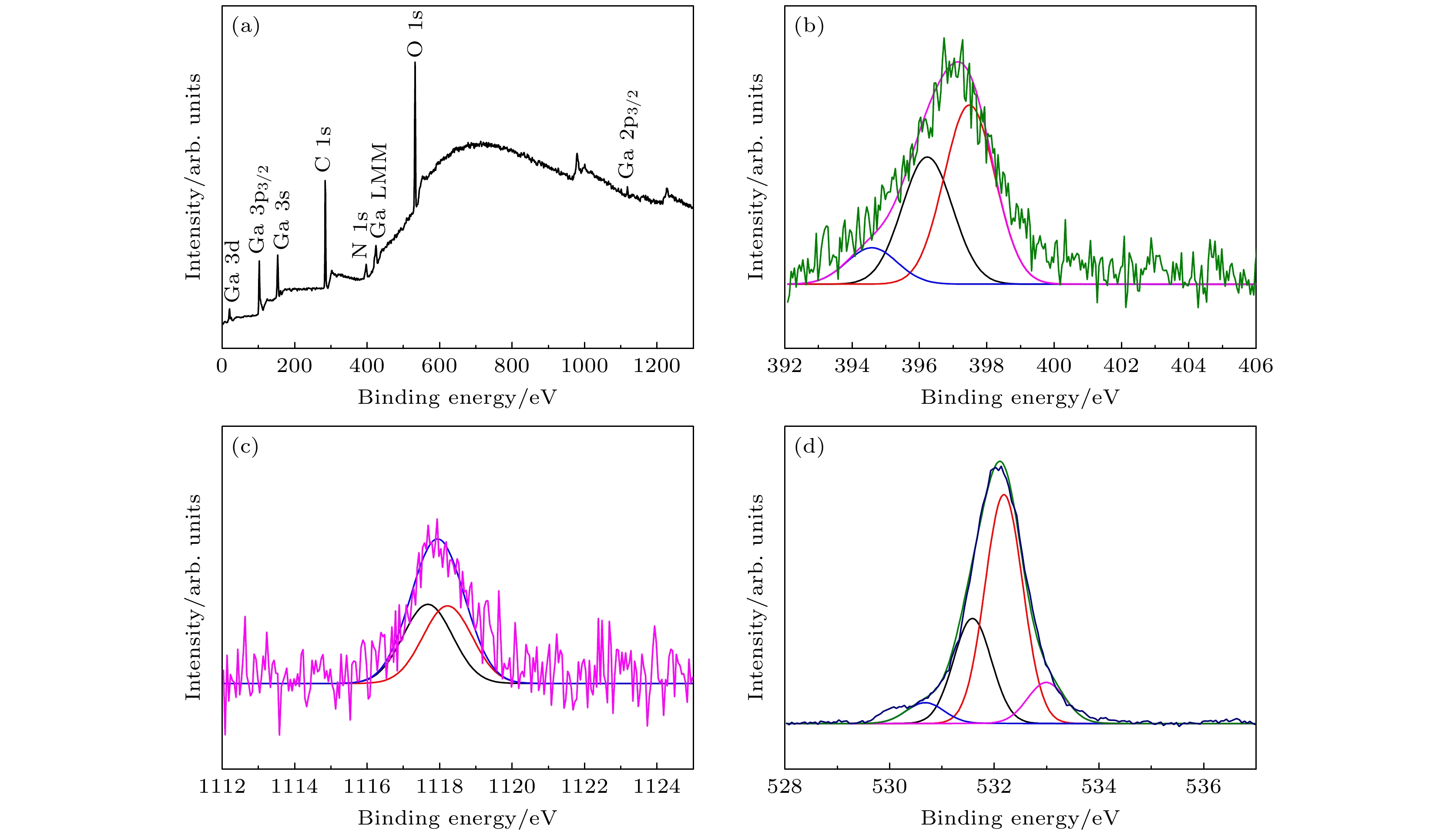
图 9 GaN薄膜的XPS图谱 (a)全谱; (b) N 1s带; (c) Ga 2p3/2带; (d) O 1s 带
Figure 9. XPS spectra of annealed GaN fim with buffer layer at 875 ℃: (a) General scan spectrum; (b) N 1s band; (c) Ga 2p3/2 band; (d) O 1s band.

图 10 GaN薄膜的UV-Vis吸收光谱.
Figure 10. UV-Vis absorption spectrum of GaN film.
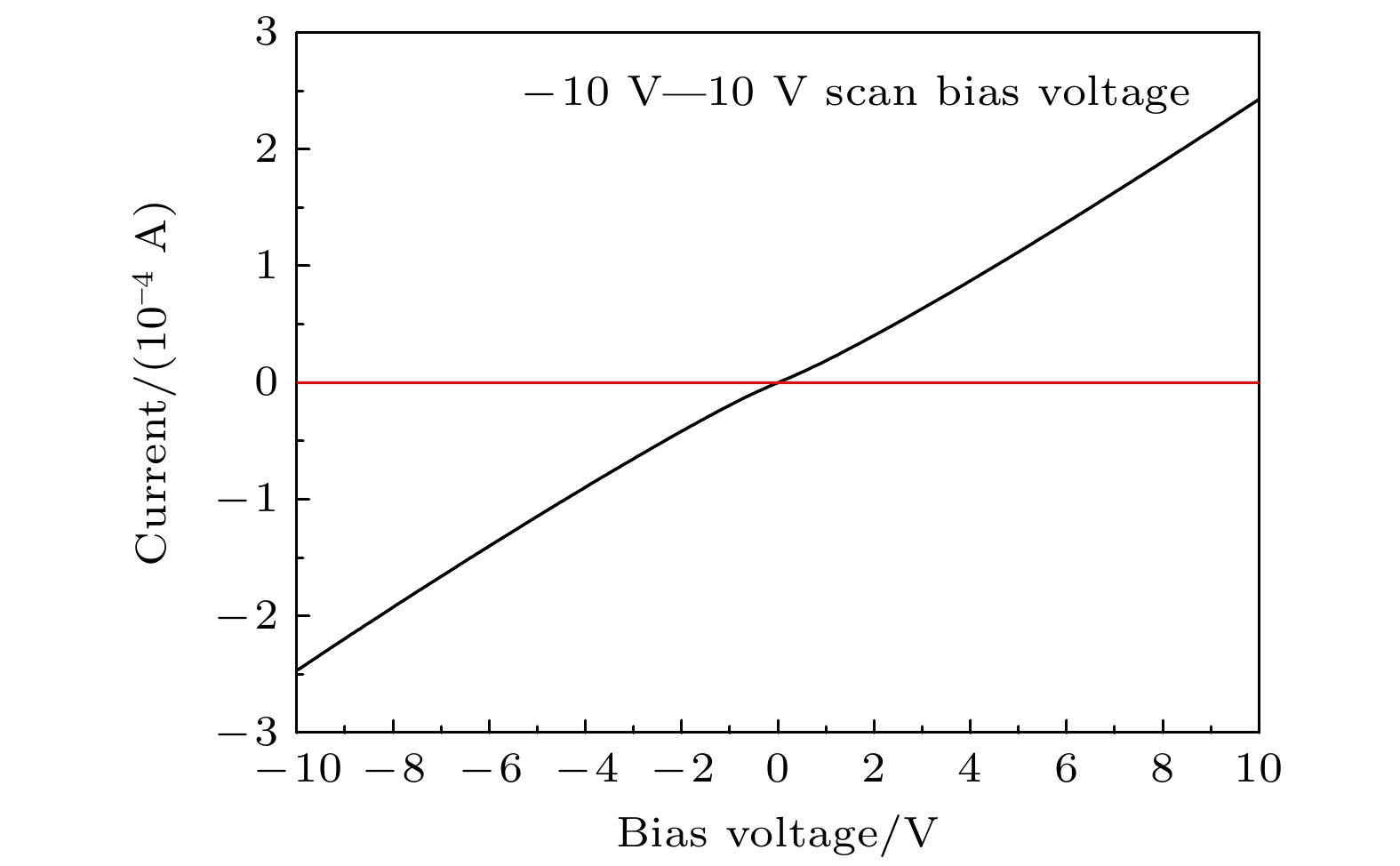
图 11 退火GaN薄膜紫外探测器的I -V曲线.
Figure 11. The I -V curve of annealed GaN film ultraviolet photodetector.

图 12 (a)退火GaN薄膜紫外探测器在不同光照强度下的光电流; (b)功率与光响应度的关系曲线
Figure 12. (a) Photocurrent of GaN film ultraviolet photodetector at different illumination intensity; (b) the power versus photoresponsivity curve of GaN fim ultraviolet photodetector.
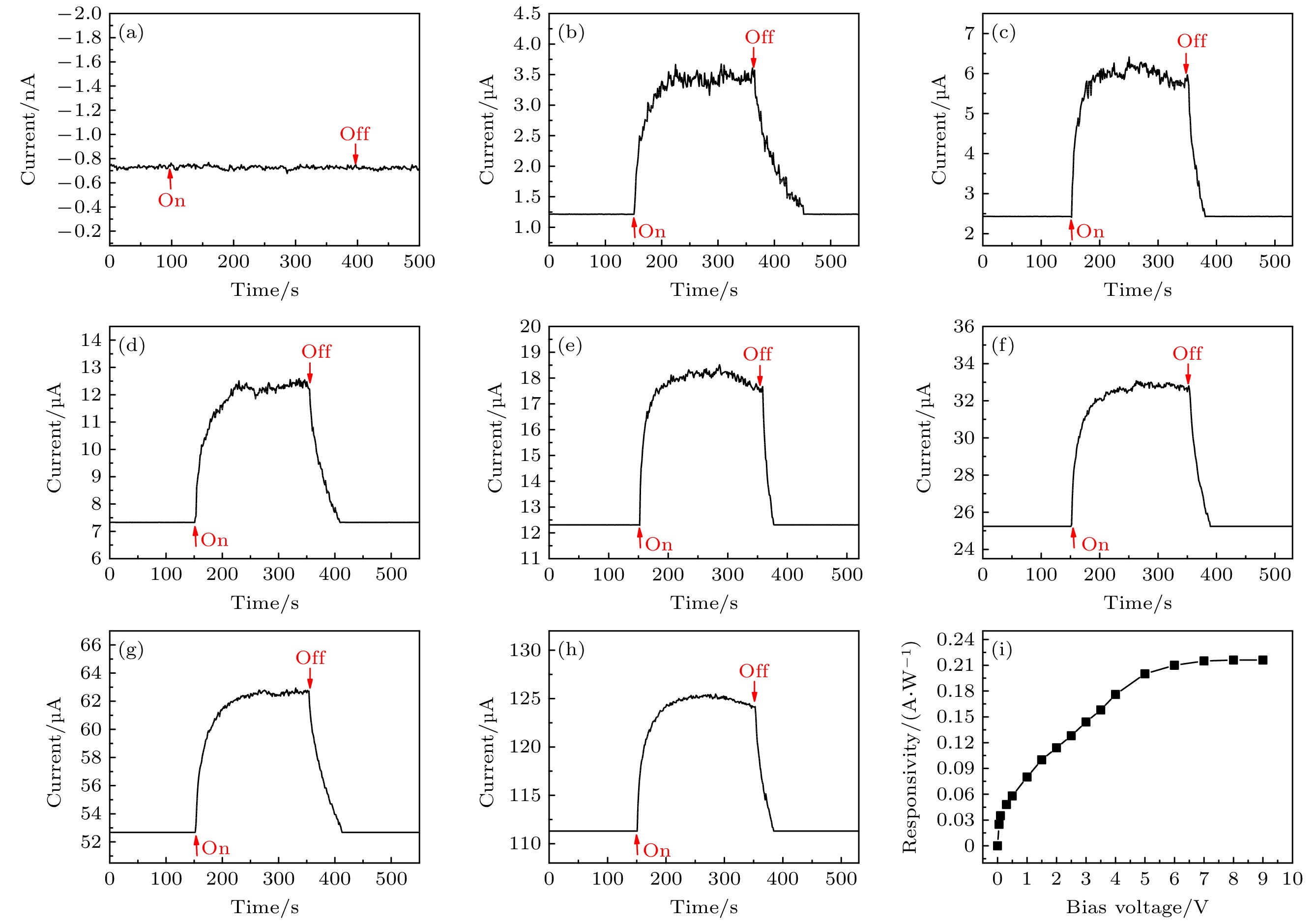
图 13 退火GaN薄膜紫外探测器在不同偏压下的电流以及光响应度 (a) 0 V; (b) 0.05 V; (c) 0.1 V; (d) 0.3 V; (e) 0.5 V; (f) 1 V; (g) 2 V; (h) 3 V; (i)不同偏压对应的光响应度大小
Figure 13. Current of annealed GaN films ultraviolet photodetector at different bias voltage: (a) 0 V; (b) 0.05 V; (c) 0.1 V; (d) 0.3 V; (e) 0.5 V; (f) 1 V; (g) 2 V; (h) 3 V. (i) The responsivity of photodetector at different bias voltage.
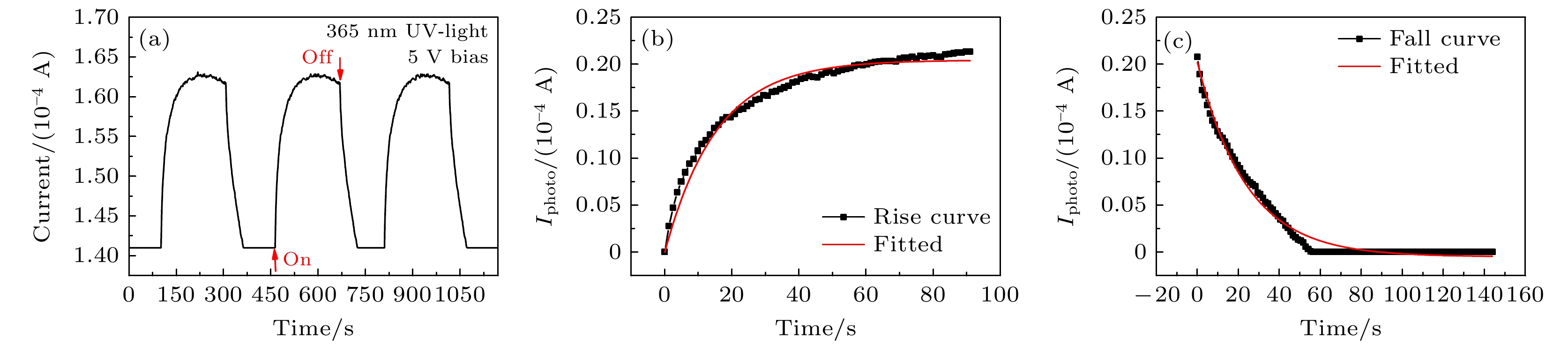
图 14 退火GaN薄膜紫外探测器 (a)电流与时间的关系曲线; (b)时间与光电流上升的曲线; (c)时间与光电流下降的曲线
Figure 14. (a) Current versus time curve of annealed GaN film ultraviolet photodetector; (b) the time versus rise current curve of annealed GaN film ultraviolet photodetector; (c) the time versus fall current curve of annealed GaN film ultraviolet photodetector.
表 1 不同缓冲层制备温度下获得的GaN薄膜的位错密度计算值
Table 1. Dislocation density of GaN films with buffer layer fabricated at different temperature.
缓冲层制备
温度/℃刃位错密度
/(109 cm–2)螺位错密度
/(109 cm–2)总位错密度
/(1010 cm–2)825 8.68 2.94 1.16 850 8.53 2.77 1.13 875 7.41 2.33 0.974 900 7.64 2.52 1.02 925 8.63 2.79 1.14  DownLoad: CSV
表 2 不同制备温度缓冲层的未退火GaN薄膜相对应的E2(high)声子散射峰半高全宽
Table 2. The full width at half maximum of E2 (high) phonon scattering peak of unannealed GaN fims with buffer layer at different temperature.
缓冲层制备温度/℃ 825 850 875 900 925 半高全宽/cm–1 18.8 13.3 10 12.5 25.2
DownLoad: CSV
表 3 缓冲层制备温度为875 ℃的GaN薄膜退火前后的Hall数据对比
Table 3. Hall value of unannealed and annealed GaN films with buffer layer at 875 ℃.
电阻率
/(Ω·cm–1)迁移率
/(cm2·V–1·s–1)载流子浓度
/(1017 cm–3)退火前 24.86 0.713 3.524 退火后 5.254 43.5 3.907
DownLoad: CSV
-
[1] Liu L, Xia S, Diao Y, Lu F, Tian J 2020 Solid State Ionics 350 115327
Google Scholar
[2] Wang X, Zhang Y, Chen X, He M, Liu C, Yin Y, Zou X, Li S 2014 Nanoscale 6 12009
Google Scholar
[3] Zhang X, Liu Q, Liu B, Yang W, Li J, Niu P, Jiang X 2017 J. Mater. Chem. C 5 4319
Google Scholar
[4] Peng M, Liu Y, Yu A, Zhang Y, Liu C, Liu J, Wu W, Zhang K, Shi X, Kou J, Zhai J, Wang Z L 2016 ACS Nano 10 1572
Google Scholar
[5] Chen X Y, Yip C T, Fung M K, Djurišić A B, Chan W K 2010 Appl. Phys. A 100 15
Google Scholar
[6] Li Y, Wang W, Li X, Huang L, Lin Z, Zheng Y, Chen X, Li G 2019 J. Alloys Compd. 771 1000
Google Scholar
[7] Deng G, Zhang Y, Yu Y, Yan L, Li P, Han X, Chen L, Zhao D, Du G 2018 Superlattice. Microstruct. 116 1
Google Scholar
[8] Liang Q, Wang R Z, Yang M Q, Ding Y, Wang C H 2020 Thin Solid Films 710 138266
Google Scholar
[9] Yang W J, Wang W L, Liu Z L, Li G Q 2015 Mater. Sci. Semicond. Process. 39 499
Google Scholar
[10] Okuno K, Oshio T, Shibata N, Honda Y, Yamaguchi M, Tanaka S, Amano H 2013 Phys. Status Solidi C 10 369
Google Scholar
[11] Bak S J, Mun D H, Jung K C, Park J H, Bae H J, Lee I W, Ha J S, Jeong T, Oh T S 2013 Electron. Mater. Lett. 9 367
Google Scholar
[12] Tran B T, Chang E Y, Lin K L, Luong T T, Yu H W, Huang M C, Chung C C, Trinh H D, Nguyen H Q, Nguyen C L, Luc Q H 2012 ECS Trans. 50 461
Google Scholar
[13] Huang W C, Chu C M, Wong Y Y, Chen K W, Lin Y K, Wu C H, Lee W I, Chang E Y 2016 Mater. Sci. Semicond. Process. 45 1
Google Scholar
[14] Zhao J W, Zhang Y F, Li Y H, Su C H, Song X M, Yan H, Wang R Z 2015 Sci. Rep. 5 17692
Google Scholar
[15] Ji Y H, Wang R Z, Feng X Y, Zhang Y F, Yan H 2017 J. Phys. Chem. C 121 24804
Google Scholar
[16] Feng X Y, Wang R Z, Liang Q, Ji Y H, Yang M Q 2019 Cryst. Growth. Des. 19 2687
Google Scholar
[17] 梁琦, 王如志, 杨孟骐, 王长昊, 刘金伟 2020 物理学报 69 087801
Google Scholar
Liang Q, Wang R Z, Yang M Q, Wang C H, Liu J W 2020 Acta Phys. Sin. 69 087801
Google Scholar
[18] Ramesh C, Tyagi P, Bhattacharyya B, Husale S, Maurya K K, Kumar M S, Kushvaha S S 2019 J. Alloys Compd. 770 572
Google Scholar
[19] Popovici G, Xu G Y, Botchkarev A, Kim W, Tang H, Salvador A, Morkoç H, Strange R, White J O 1997 J. Appl. Phys. 82 4020
Google Scholar
[20] Eckey L, Gfug U V, Holst J, Hoffmann A, Kaschner A, Siegle H, Thomsen C, Schineller B, Heime K, Heuken M, Schön O, Beccard R 1998 J. Appl. Phys. 84 5828
Google Scholar
[21] Greenlee J D, Feigelson B N, Anderson T J, Tadjer M J, Hite J K, Mastro M A, Eddy C R, Hobart K D, Kub F J 2014 J. Appl. Phys. 116 063502
Google Scholar
[22] Huang Y, Chen X D, Fung S, Beling C D, Ling C C, Wei Z F, Xu S J, Zhi C Y 2004 J. Appl. Phys. 96 1120
Google Scholar
[23] Hwang C Y, Schurman M J, Mayo W E 1997 J. Electron. Mater. 26 243
Google Scholar
[24] Jeong J K, Choi J H, Hwang C S, Kim H J, Lee J H, Lee J H, Kim C S 2004 Appl. Phys. Lett. 84 2575
Google Scholar
[25] Ng H M, Doppalapudi D, Moustakas T D, Weimann N G, Eastman L F 1998 Appl. Phys. Lett. 73 821
Google Scholar
[26] Lee J H, Hahm S H, Lee J H, Bae S B, Lee K S, Cho Y H, Lee J L 2003 Appl. Phys. Lett. 83 917
Google Scholar
[27] Wang Y Q, Wang R Z, Zhu M K, Wang B B, Wang B, Yan H 2013 Appl. Surf. Sci. 285 115
Google Scholar
[28] Lee C T, Lin Y J, Lin C H 2002 J. Appl. Phys. 92 3825
Google Scholar
[29] Gui Y, Yang L, Tian K, Zhang H, Fang S 2019 Sens. Actuators, B 288 104
Google Scholar
[30] Sun X, Li D, Jiang H, Li Z, Song H, Chen Y, Miao G 2011 Appl. Phys. Lett. 98 121117
Google Scholar
[31] Jhou Y D, Chang S J, Su Y K, Lee Y Y, Liu C H, Lee H C 2007 Appl. Phys. Lett. 91 103506
Google Scholar
[32] Golgir H R, Li D W, Keramatnejad K, Zou Q M, Xiao J, Wang F, Jiang L, Silvain J F, Lu Y F 2017 ACS Appl. Mater. Interfaces 9 21539
Google Scholar
[33] Müller A, Konstantinidis G, Androulidaki M, Dinescu A, Stefanescu A, Cismaru A, Neculoiu D, Pavelescu E, Stavrinidis A 2012 Thin Solid Films 520 2158
Google Scholar
[34] Xie F, Lu H, Xiu X, Chen D, Han P, Zhang R, Zheng Y 2011 Solid State Electron. 57 39
Google Scholar
[35] Osinsky A, Gangopadhyay S, Yang J W, Gaska R, Kuksenkov D, Temkin H, Shmagin I K, Chang Y C, Muth J F, Kolbas R M 1998 Appl. Phys. Lett. 72 551
Google Scholar
[36] Pant R, Shetty A, Chandan G, Roul B, Nanda K K, Krupanidhi S B 2018 ACS Appl. Mater. Interfaces 10 16918
Google Scholar
[37] Mukundan S, Mohan L, Chandan G, Roul B, Krupanidhi S B 2014 J. Appl. Phys. 116 204502
Google Scholar

 DownLoad:
Catalog
Metrics
- Abstract views: 4179
- PDF Downloads: 115
- Cited By: 0
