


-
In tunneling oxide passivation contact (n-TOPCon) photovoltaic devices, poly-Si (n+) films with high-concentration phosphorus doping are the key materials for electron selective passivation. Its optical and electronic properties strongly depend on the chemical configuration and physical phase, and also on high temperature annealing and structural relaxation in the recrystallization process. The poly-Si (n+) films grown on SiOx/n-Si substrates by low pressure chemical vapor deposition technology are investigated, while the microstructure of the film is studied by using X-ray photoelectron spectroscopy with depth etching, high-resolution transmission electron microscopy and X-ray diffraction analysis. It is found that the binding energy values of the two fitted peaks (O2 and O3) of O 1s state of the thin film are situated at 532.1 and 533.7 eV, corresponding to the bonding of O—Si and O—P, respectively. The binding energy values of the two fitted peaks (P2 and P3) of P 2p state are located at 132.4 and 135.1 eV, corresponding to O—P* bonding with the same origin. Electronic microscopy and light diffraction analyses show that the polycrystalline silicon film has the characteristic of (111) preferential orientation, and the space of crystal plane is 0.313 nm, for which the average grain size is in a range of about 43.6–55.0 nm. However, the mechanical deformation and grain boundaries are generated in the annealing process at 920 ℃ along (111) crystal cluster, resulting in the localized monocrystalline state within large grains. The comprehensive analyses of thermodynamic function parameters of formation enthalpy, reaction entropy, heat capacity, formation energy and Gibbs free energy and energy minimum principle analysis indicate that there exist conditions for forming Si—O and P—O bonds in the polysilicon film, and thus the bonding state of silicon and phosphorus oxides are formed.
-
Keywords:
- poly-Si (n+) /
- phosphorous oxide /
- silicon oxide /
- photoelectron spectroscopy /
- depth profile analysis
[1] Feldmann F, Bivour M, Reichel C, Steinkemper H, Hermle M, Glunz S W 2014 Sol. Energy Mater. Sol. Cells 131 46
 Google Scholar
[2] Moldovan A, Feldmann F, Zimmer M, Rentsch J, Benick J, Hermle M 2015 Sol. Energy Mater. Sol. Cells 142 123
Google Scholar
[3] Shen W, Zhao Y, Liu F 2022 Front. Energy 16 40
Google Scholar
[4] Richter A, Müller R, Benick J, Feldmann F, Steinhauser B, Reichel C, Fell A, Bivour M, Hermle M, Glunz S W 2021 Nat. Energy 6 429
Google Scholar
[5] Long W, Yin S, Peng F G, Yang M, Fang L, Ru X N, Qu M H, Lin H F, Xu X X 2021 Sol. Energy Mater. Sol. Cells 231 111291
Google Scholar
[6] Yan D, Cuevas A, Michel J I, Zhang C, Wan Y, Zhang X, Bullock J 2021 Joule 5 811
Google Scholar
[7] Chen D, Chen Y, Wang Z, Gong J, Liu C, Zou Y, He Y, Wang Y, Yuan L, Lin W, Xia R, Yin L, Zhang X, Xu G, Yang Y, Shen H, Feng Z, Altermatt P P, Verlinden P J 2020 Sol. Energy Mater. Sol. Cells 206 110258
Google Scholar
[8] Yoshikawa K, Kawasaki H, Yoshida W, Irie T, Konishi K, Nakano K, Uto T, Adachi D, Kanematsu M, Uzu H 2017 Nat. Energy 2 17032
Google Scholar
[9] Chandra M N, Biswas S, Acharya S, Panda T, Sadhukhan S, Sharma J R, Nandi A, Bose S, Kole A, Das G, Maity S, Chaudhuri P, Saha H 2020 Mater. Sci. Semicond. Process. 119 105163
Google Scholar
[10] Padhamnath P, Khanna A, Nandakumar N, Nampalli N, Shanmugam V, Aberle A G, Duttagupta S 2020 Sol. Energy Mater. Sol. Cells 207 110358
Google Scholar
[11] Gao T, Yang Q, Guo X Q, Huang Y Q, Zhang Z, Wang Z X, Liao M D, Shou C H, Zeng Y H, Yan B J, Hou G F, Zhang X D, Zhao Y, Ye J C 2019 Sol. Energy Mater. Sol. Cells 200 109926
Google Scholar
[12] Kim D R, Lee C H, Weisse J M, Cho I S, Zheng X 2012 Nano Lett. 12 6485
Google Scholar
[13] Polzin J I, Hammann B, Niewelt T, Kwapil W, Hermle M, Feldmann F 2021 Sol. Energy Mater. Sol. Cells 230 111267
Google Scholar
[14] Padhamnath P, Khanna A, Balaji N, Shanmugam V, Nandakumar N, Wang D, Sun Q, Huang M, Huang S, Fan B, Ding B, Aberle A G, Duttagupta S 2020 Sol. Energy Mater. Sol. Cells 218 110751
Google Scholar
[15] Susa M, Kawagishi K, Tanaka N, Nagata K 1997 J. Electrochem. Soc. 144 2552
Google Scholar
[16] Hide I, Matsuyama T, Suzuki M, Yamashita H, Suzuki T, Moritani T, Maeda Y 1990 J. Cryst. Growth 99 1339
Google Scholar
[17] Fırat M, Payo M R, Duerinckx F, Luchies J-M, Lenes M, Poortmans J 2019 AIP Conf. Proc. 2147 040004
Google Scholar
[18] Kern W 1970 RCA Rev. 31 51
Google Scholar
[19] Lozac'h M, Nunomura S, Matsubara K 2020 Sol. Energy Mater. Sol. Cells 207 110357
Google Scholar
[20] Han L, Chen Z 2013 ECS J. Solid State Sci. Technol. 2 N228
Google Scholar
[21] Ying W B, Mizokawa Y, Kamiura Y, Kawamoto K, Yang W Y 2001 Appl. Surf. Sci. 181 1
Google Scholar
[22] Sherwood P M A 2002 Surf. Sci. Spectra 9 62
Google Scholar
[23] Moulder J F, Chastain J, King R C 1992 Handbook of X-ray Photoelectron Spectroscopy: a Reference Book of Standard Spectra for Identification and Interpretation of XPS Data (Waltham: Perkin-Elmer Corporation) pp230–232
[24] Chen K, Bothwell A, Guthrey H, Hartenstein M B, Polzin J I, Feldmann F, Nemeth W, Theingi S, Page M, Young D L, Stradins P, Agarwal S 2022 Sol. Energy Mater. Sol. Cells 236 111510
Google Scholar
[25] Monshi A, Foroughi M R, Monshi M R 2012 World J. Nano Sci. Eng. 2 154
Google Scholar
[26] Kale A S, Nemeth W, Guthrey H, Nanayakkara S U, LaSalvia V, Theingi S, Findley D, Page M, Al-Jassim M, Young D L, Stradins P, Agarwal S 2019 ACS Appl. Mater. Interfaces 11 42021
Google Scholar
[27] De Jong M, Chen W, Angsten T, Jain A, Notestine R, Gamst A, Sluiter M, Krishna Ande C, van der Zwaag S, Plata J J, Toher C, Curtarolo S, Ceder G, Persson K A, Asta M 2015 Sci. Data 2 150009
Google Scholar
[28] De Jong M, Chen W, Geerlings H, Asta M, Persson K A 2015 Sci. Data 2 150053
Google Scholar
[29] Jain A, Hautier G, Ong S P, Moore C J, Fischer C C, Persson K A, Ceder G 2011 Phys. Rev. B 84 045115
Google Scholar
[30] Perry D L, Phillips S L 1998 Handbook of inorganic compounds (Boca Raton: CRC Press)
[31] Jung I H, Hudon P 2012 J. Am. Ceram. Soc. 95 3665
Google Scholar
[32] Rahman M, Hudon P, Jung I H 2013 Metall. Mater. Trans. B 44 837
Google Scholar
[33] Boigelot R, Graz Y, Bourgel C, Defoort F, Poirier J 2015 Ceram. Int. 41 2353
Google Scholar
-
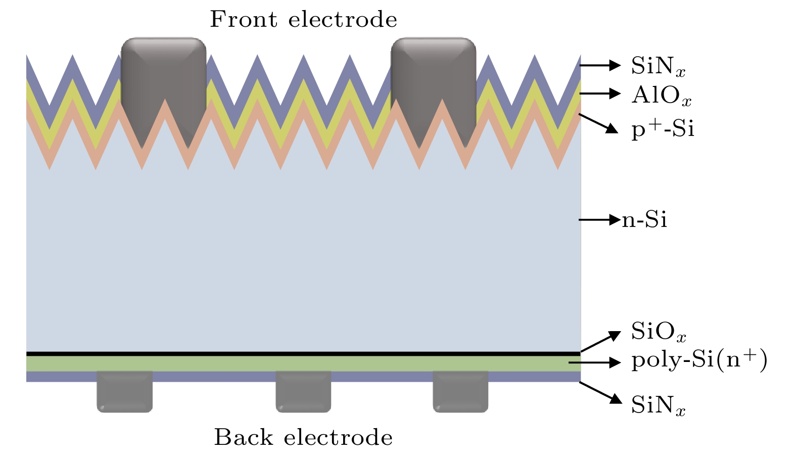
图 1 n-TOPCon 器件结构示意图
Figure 1. Schematic diagram of n-TOPCon device.
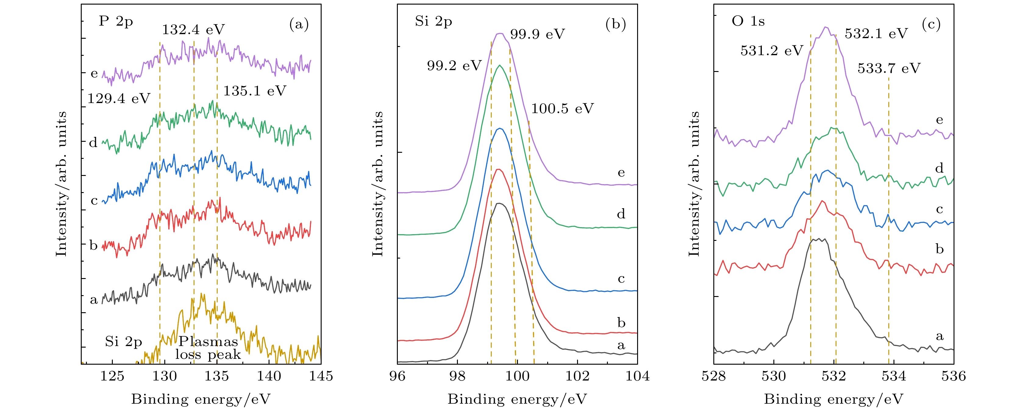
图 2 P 2p, Si 2p, O 1s态的XPS能谱图(描述了能谱在薄膜不同深度处的强度变化, 对应刻蚀时间为a: 0 s, b: 500 s, c: 1500 s, d: 2000 s, e: 2600 s) (a) P 2p态的XPS能谱和Si 2p态的等离激元损失峰; (b) Si 2p 态的XPS能谱; (c) O 1s 态的XPS能谱. 为了方便显示各元素结合能的变化, 对(a)—(c)图谱曲线的强度均做出了调整
Figure 2. The XPS spectra of P 2p, Si 2p and O 1s, which describes the changes of density with different depths at etching time of a 0 s, b 500 s, c 1500 s, d 2000 s, and e 2600 s. (a) XPS spectra of P 2p states and Si 2p for plasmon loss peak; (b) XPS spectra of Si 2p states; (c) XPS spectra of O 1s states. In order to display the change of binding energy of each elements intuitively, the intensity of spectrum curves in panel (a)–(c) are adjusted.
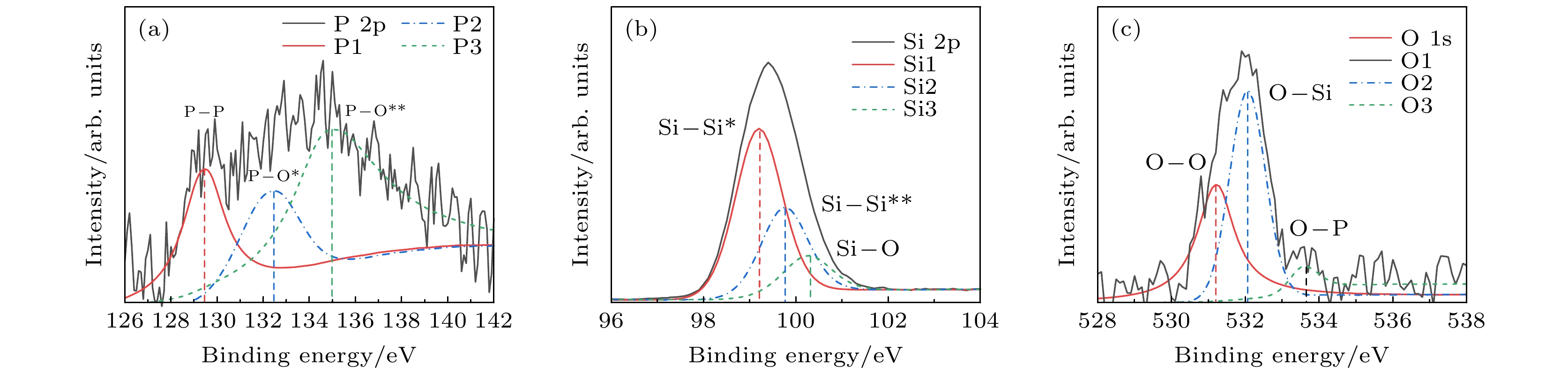
图 3 刻蚀时间为2000 s时P 2p态、Si 2p、O 1s态的分峰拟合图谱 (a) P 2p态; (b) Si 2p态; (c) O 1s态
Figure 3. Fitting peak spectra of P 2p, Si 2p, O 1s state of etching time of 2000 s: (a) P 2p state; (b) Si 2p state; (c) O 1s state.
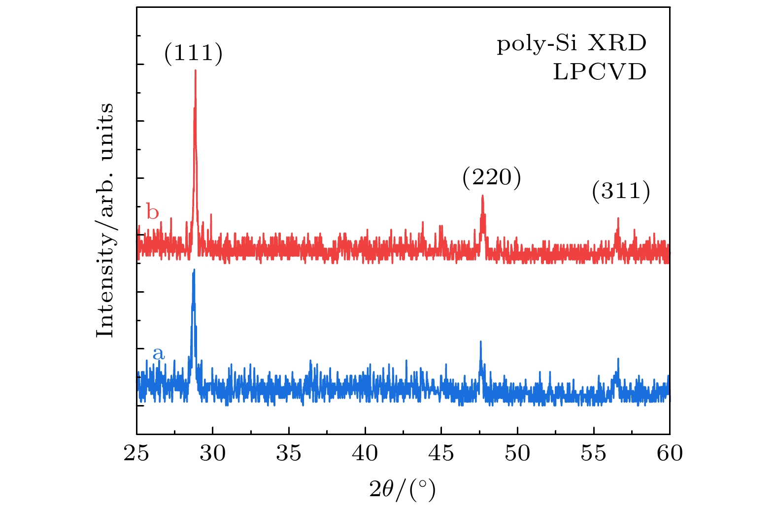
图 4 n-TOPCon器件中poly-Si (n+)薄膜的XRD表征, 其中a, b分别为同一样品的两次测量结果
Figure 4. Characterization of poly-Si (n+) film in n-TOPCon device, and a, b are the two measurements for the same sample, respectively.
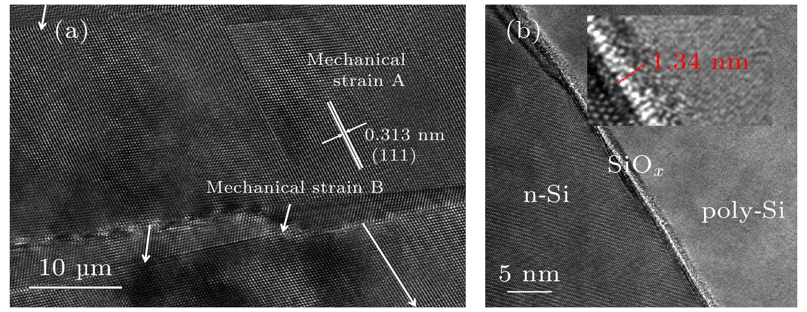
图 5 (a) n-TOPCon器件中poly-Si (n+)薄膜的不同晶面方向与力学形变; (b) poly-Si (n+)/SiOx/n-Si界面与隧穿氧化硅
Figure 5. (a) Characterization of different crystal face orientations and mechanical strains in poly-Si (n+) film of n-TOPCon device; (b) poly-Si (n+)/SiOx/n-Si interface and tunneling silicon oxide.
表 1 298 K(室温)时, SiP, SiO, SiO2 和P2O5的热力学函数参数(生成焓、热容、反应熵与形成能)
Table 1. Thermodynamic function parameters (formation enthalpy, heat capacity, reaction entropy and formation energy) of SiP, SiO, SiO2 and P2O5 at 298 K (RT).
$ {H}_{0}^{298} $/
eV${C}_{\mathrm{P} }$/
(J·mol–1·K–1)${ {S} }_{0}^{298}/$
(J·mol–1·K–1)形成能/
eVSiP –0.64 –5.65 33.35 –0.28 SiO –8.19 –2.05 211.18 –4.11 SiO2 –9.44 –10.08 43.63 –9.81 P2O5 –31.20 –15.61 17.07 –15.60  DownLoad: CSV
表 2 1193 K (920 ℃)时, SiP, SiO, SiO2 和 P2O5的热力学函数参数(生成焓、热容、反应熵与形成能)
Table 2. Thermodynamic function parameters (formation enthalpy, heat capacity, reaction entropy and Gibbs free energy) of SiP, SiO, SiO2 and P2O5 at 1193 K.
$ {H}_{0}^{1193} $/
eV$ {C}_{\mathrm{P}} $/
(J·mol–1·K–1)$ {S}_{0}^{1193} $/
(J·mol–1·K–1)$ {G}_{0}^{1193} $
/
eVSiP –53.05 –5.65 25.51 –53.37 SiO –27.21 –2.05 208.34 –29.79 SiO2 –102.95 –10.08 29.65 –103.31 P2O5 –176.01 –15.61 –4.58 –175.95
DownLoad: CSV
-
[1] Feldmann F, Bivour M, Reichel C, Steinkemper H, Hermle M, Glunz S W 2014 Sol. Energy Mater. Sol. Cells 131 46
Google Scholar
[2] Moldovan A, Feldmann F, Zimmer M, Rentsch J, Benick J, Hermle M 2015 Sol. Energy Mater. Sol. Cells 142 123
Google Scholar
[3] Shen W, Zhao Y, Liu F 2022 Front. Energy 16 40
Google Scholar
[4] Richter A, Müller R, Benick J, Feldmann F, Steinhauser B, Reichel C, Fell A, Bivour M, Hermle M, Glunz S W 2021 Nat. Energy 6 429
Google Scholar
[5] Long W, Yin S, Peng F G, Yang M, Fang L, Ru X N, Qu M H, Lin H F, Xu X X 2021 Sol. Energy Mater. Sol. Cells 231 111291
Google Scholar
[6] Yan D, Cuevas A, Michel J I, Zhang C, Wan Y, Zhang X, Bullock J 2021 Joule 5 811
Google Scholar
[7] Chen D, Chen Y, Wang Z, Gong J, Liu C, Zou Y, He Y, Wang Y, Yuan L, Lin W, Xia R, Yin L, Zhang X, Xu G, Yang Y, Shen H, Feng Z, Altermatt P P, Verlinden P J 2020 Sol. Energy Mater. Sol. Cells 206 110258
Google Scholar
[8] Yoshikawa K, Kawasaki H, Yoshida W, Irie T, Konishi K, Nakano K, Uto T, Adachi D, Kanematsu M, Uzu H 2017 Nat. Energy 2 17032
Google Scholar
[9] Chandra M N, Biswas S, Acharya S, Panda T, Sadhukhan S, Sharma J R, Nandi A, Bose S, Kole A, Das G, Maity S, Chaudhuri P, Saha H 2020 Mater. Sci. Semicond. Process. 119 105163
Google Scholar
[10] Padhamnath P, Khanna A, Nandakumar N, Nampalli N, Shanmugam V, Aberle A G, Duttagupta S 2020 Sol. Energy Mater. Sol. Cells 207 110358
Google Scholar
[11] Gao T, Yang Q, Guo X Q, Huang Y Q, Zhang Z, Wang Z X, Liao M D, Shou C H, Zeng Y H, Yan B J, Hou G F, Zhang X D, Zhao Y, Ye J C 2019 Sol. Energy Mater. Sol. Cells 200 109926
Google Scholar
[12] Kim D R, Lee C H, Weisse J M, Cho I S, Zheng X 2012 Nano Lett. 12 6485
Google Scholar
[13] Polzin J I, Hammann B, Niewelt T, Kwapil W, Hermle M, Feldmann F 2021 Sol. Energy Mater. Sol. Cells 230 111267
Google Scholar
[14] Padhamnath P, Khanna A, Balaji N, Shanmugam V, Nandakumar N, Wang D, Sun Q, Huang M, Huang S, Fan B, Ding B, Aberle A G, Duttagupta S 2020 Sol. Energy Mater. Sol. Cells 218 110751
Google Scholar
[15] Susa M, Kawagishi K, Tanaka N, Nagata K 1997 J. Electrochem. Soc. 144 2552
Google Scholar
[16] Hide I, Matsuyama T, Suzuki M, Yamashita H, Suzuki T, Moritani T, Maeda Y 1990 J. Cryst. Growth 99 1339
Google Scholar
[17] Fırat M, Payo M R, Duerinckx F, Luchies J-M, Lenes M, Poortmans J 2019 AIP Conf. Proc. 2147 040004
Google Scholar
[18] Kern W 1970 RCA Rev. 31 51
Google Scholar
[19] Lozac'h M, Nunomura S, Matsubara K 2020 Sol. Energy Mater. Sol. Cells 207 110357
Google Scholar
[20] Han L, Chen Z 2013 ECS J. Solid State Sci. Technol. 2 N228
Google Scholar
[21] Ying W B, Mizokawa Y, Kamiura Y, Kawamoto K, Yang W Y 2001 Appl. Surf. Sci. 181 1
Google Scholar
[22] Sherwood P M A 2002 Surf. Sci. Spectra 9 62
Google Scholar
[23] Moulder J F, Chastain J, King R C 1992 Handbook of X-ray Photoelectron Spectroscopy: a Reference Book of Standard Spectra for Identification and Interpretation of XPS Data (Waltham: Perkin-Elmer Corporation) pp230–232
[24] Chen K, Bothwell A, Guthrey H, Hartenstein M B, Polzin J I, Feldmann F, Nemeth W, Theingi S, Page M, Young D L, Stradins P, Agarwal S 2022 Sol. Energy Mater. Sol. Cells 236 111510
Google Scholar
[25] Monshi A, Foroughi M R, Monshi M R 2012 World J. Nano Sci. Eng. 2 154
Google Scholar
[26] Kale A S, Nemeth W, Guthrey H, Nanayakkara S U, LaSalvia V, Theingi S, Findley D, Page M, Al-Jassim M, Young D L, Stradins P, Agarwal S 2019 ACS Appl. Mater. Interfaces 11 42021
Google Scholar
[27] De Jong M, Chen W, Angsten T, Jain A, Notestine R, Gamst A, Sluiter M, Krishna Ande C, van der Zwaag S, Plata J J, Toher C, Curtarolo S, Ceder G, Persson K A, Asta M 2015 Sci. Data 2 150009
Google Scholar
[28] De Jong M, Chen W, Geerlings H, Asta M, Persson K A 2015 Sci. Data 2 150053
Google Scholar
[29] Jain A, Hautier G, Ong S P, Moore C J, Fischer C C, Persson K A, Ceder G 2011 Phys. Rev. B 84 045115
Google Scholar
[30] Perry D L, Phillips S L 1998 Handbook of inorganic compounds (Boca Raton: CRC Press)
[31] Jung I H, Hudon P 2012 J. Am. Ceram. Soc. 95 3665
Google Scholar
[32] Rahman M, Hudon P, Jung I H 2013 Metall. Mater. Trans. B 44 837
Google Scholar
[33] Boigelot R, Graz Y, Bourgel C, Defoort F, Poirier J 2015 Ceram. Int. 41 2353
Google Scholar

 DownLoad:
Catalog
Metrics
- Abstract views: 3888
- PDF Downloads: 104
- Cited By: 0
