


-
二维六方氮化硼(hBN)的点缺陷最近被发现可以实现室温下的单光子发射, 而成为近年的研究热点. 尽管其具有重要的基础和应用研究意义, hBN中发光缺陷的原子结构起源仍然存在争议. 本文采用基于密度泛函理论的第一性原理计算, 研究hBN单层中一种B空位附近3个N原子被C替代的缺陷(CN)3VB. 在hBN的B空位处, 3个N原子各自带一个在平面内的悬挂键及相应的未配对电子, 而通过C替换可以消除未配对的电子. 系统研究了(CN)3VB缺陷的几何结构、电子结构以及光学性质, 结果表明, 缺陷可以由一个对称的亚稳态经过原子结构弛豫变成1个非对称的、3个C原子连在一起的基态结构. 缺陷的形成在hBN中引入了一些由缺陷悬挂σ键及重构的π键贡献的局域缺陷态. 这些缺陷态可以导致能量阈值在2.58 eV附近的可见光内部跃迁. 本文的工作有助于进一步理解hBN中点缺陷的构成及光学性质, 为实验上探讨发光点缺陷的原子结构起源及其性质提供理论依据.The point defect of two-dimensional hexagonal boron nitride (hBN) has recently been discovered to achieve single photon emission at room temperature, and it has become a research hotspot. Despite its important fundamental and applied research significance, the origin of the atomic structure of luminescence defects in hBN is still controversial. In this paper, first-principle calculations based on density functional theory are used to study a defect (CN)3VB in the hexagonal boron nitride monolayer (hBN) where three N atoms near the B vacancy are replaced by C atoms. At the B vacancy of hBN, the three N atoms each carry an in-plane dangling bond and the corresponding unpaired electron, and the unpaired electron can be eliminated by C substitution. We systematically study the geometric structure, electronic structure and optical properties of (CN)3VB defects, analyze the thermodynamic stability of defects through the calculation of the atomic structure, formation energy, and charge state of the defect, and analyze the position in the band gap and its atomic orbital contribution of defect state through energy band structure and wave function. We also analyze its optical properties through dielectric function and absorption coefficient, and predict its luminous photon energy. The results show that the defect can change from a symmetric metastable state to an asymmetric ground state structure with three C atoms connected together through atomic structure relaxation. The formation energy of asymmetric (CN)3VB is 7.94 eV, which is 3.72 eV lower than that of symmetric one. The formation of defects introduces some local defect states contributed by defect dangling σ bonds and reconstructed π bonds in hBN. The defects have valence states between –2 and +2, and the thermodynamic transition energy level of asymmetric (CN)3VB is higher than that of symmetric (CN)3VB. In the transition from the metastable state to the ground state, these defect states can redshift the light absorption boundary of hBN, enhance the absorption intensity of visible light by hBN, and cause internal optical transitions. Among them, there is a visible light transition with an energy threshold around 2.58 eV in the asymmetry (CN)3VB defect. Single boron atom vacancy defect and (CN)3VB have optical transitions near infrared and ultraviolet energy, respectively. The present work will help to further understand the composition and optical properties of point defects in hBN, and provide a theoretical basis for experimentally exploring the origin and properties of the atomic structure of light-emitting point defects.
[1] Lee S, Yeo J S, Ji Y, Cho C, Kim D Y, Na S I, Lee B H, Lee T 2012 Nanotechnology 23 344013
 Google Scholar
[2] Abderrahmane A, Ko P J, Thu T V, Ishizawa S, Takamura T, Sandhu A 2014 Nanotechnology 25 365202
Google Scholar
[3] Li X, Yin J, Zhou J, Wang Q, Guo W 2014 Nanotechnology 25 105701
Google Scholar
[4] Abdi M, Degenfeld-Schonburg P, Sameti M, Navarrete-Benlloch C, Hartmann M J 2016 Phys. Rev. Lett. 116 233604
Google Scholar
[5] Xia F, Wang H, Xiao D, Dubey M, Ramasubramaniam A 2014 Nat. Photonics 8 899
Google Scholar
[6] Clark G, Schaibley J R, Ross J, Taniguchi T, Watanabe K, Hendrickson J R, Mou S, Yao W, Xu X 2016 Nano Lett. 16 3944
Google Scholar
[7] Shiue R J, Efetov D K, Grosso G, Peng C, Fong K C, Englund D 2017 Nanophotonics 6 1329
Google Scholar
[8] Koenderink A F, Alu A, Polman A 2015 Science 348 516
Google Scholar
[9] Caldwell J D, Aharonovich I, Cassabois G, Edgar J H, Gil B, Basov D 2019 Nat. Rev. Mater. 4 552
Google Scholar
[10] Cai J, Retzker A, Jelezko F, Plenio M B 2013 Nat. Phys. 9 168
Google Scholar
[11] Pla J J, Tan K Y, Dehollain J P, Lim W H, Morton J J, Jamieson D N, Dzurak A S, Morello A 2012 Nature 489 541
Google Scholar
[12] Scarani V, Bechmann-Pasquinucci H, Cerf N J, Dušek M, Lütkenhaus N, Peev M 2009 Rev. Mod. Phys. 81 1301
Google Scholar
[13] O’brien J L, Furusawa A, Vučković J 2009 Nat. Photonics 3 687
Google Scholar
[14] Lo H K, Curty M, Tamaki K 2014 Nat. Photonics 8 595
Google Scholar
[15] Cheung J, Chunnilall C, Woolliams E, Fox N, Mountford J, Wang J, Thomas P 2007 J. Mod. Opt. 54 373
Google Scholar
[16] Rose B C, Huang D, Zhang Z H, Stevenson P, Tyryshkin A M, Sangtawesin S, Srinivasan S, Loudin L, Markham M L, Edmonds A M, Twitchen D J, Lyon S A, de Leon N P 2018 Science 361 60
Google Scholar
[17] Chen D, Zheludev N, Gao W B 2020 Adv. Quantum Technol. 3 1900069
Google Scholar
[18] Bradac C, Gao W, Forneris J, Trusheim M E, Aharonovich I 2019 Nat. Commun. 10 5625
Google Scholar
[19] Tran T T, Bray K, Ford M J, Toth M, Aharonovich I 2015 Nat. Nanotechnol. 11 37
Google Scholar
[20] Chakraborty C, Kinnischtzke L, Goodfellow K M, Beams R, Vamivakas A N 2015 Nat. Nanotechnol. 10 507
Google Scholar
[21] He Y M, Clark G, Schaibley J R, He Y, Chen M C, Wei Y J, Ding X, Zhang Q, Yao W, Xu X 2015 Nat. Nanotechnol. 10 497
Google Scholar
[22] Koperski M, Nogajewski K, Arora A, Cherkez V, Mallet P, Veuillen J Y, Marcus J, Kossacki P, Potemski M 2015 Nat. Nanotechnol. 10 503
Google Scholar
[23] Kumar S, Kaczmarczyk A, Gerardot B D 2015 Nano Lett. 15 7567
Google Scholar
[24] Srivastava A, Sidler M, Allain A V, Lembke D S, Kis A, Imamoglu A 2015 Nat. Nanotechnol. 10 491
Google Scholar
[25] Tonndorf P, Schmidt R, Schneider R, Kern J, Buscema M, Steele G A, Castellanos-Gomez A, van der Zant H S, Vasconcellos S M, Bratschitsch R 2015 Optica 2 347
Google Scholar
[26] Kern J, Niehues I, Tonndorf P, Schmidt R, Wigger D, Schneider R, Stiehm T, de Vasconcellos M S, Reiter D E, Kuhn T, Bratschitsch R 2016 Adv. Mater. 28 7101
Google Scholar
[27] Liu X, Hersam M C 2019 Nat. Rev. Mater. 4 669
Google Scholar
[28] Chen X, Lu X, Dubey S, Yao Q, Liu S, Wang X, Xiong Q, Zhang L, Srivastava A 2019 Nat. Phys. 15 221
Google Scholar
[29] Ziegler J, Klaiss R, Blaikie A, Miller D, Horowitz V R, Alemán B J 2019 Nano Lett. 19 2121
Google Scholar
[30] Chejanovsky N, Kim Y, Zappe A, Stuhlhofer B, Taniguchi T, Watanabe K, Dasari D, Finkler A, Smet J H, Wrachtrup J 2017 Sci. Rep. 7 14758
Google Scholar
[31] Jungwirth N R, Calderon B, Ji Y, Spencer M G, Flatte M E, Fuchs G D 2016 Nano Lett. 16 6052
Google Scholar
[32] Tran T T, Elbadawi C, Totonjian D, Lobo C J, Grosso G, Moon H, Englund D R, Ford M J, Aharonovich I, Toth M 2016 ACS Nano 10 7331
Google Scholar
[33] Dietrich A, Burk M, Steiger E S, Antoniuk L, Tran T T, Nguyen M, Aharonovich I, Jelezko F, Kubanek A 2018 Phys. Rev. B 98 081414
Google Scholar
[34] Meyer J C, Chuvilin A, Algara-Siller G, Biskupek J, Kaiser U 2009 Nano Lett. 9 2683
Google Scholar
[35] Alem N, Erni R, Kisielowski C, Rossell M D, Gannett W, Zettl A 2009 Phys. Rev. B 80 155425
Google Scholar
[36] Watanabe K, Taniguchi T, Kanda H 2004 Nat. Mater. 3 404
Google Scholar
[37] Kubota Y, Watanabe K, Tsuda O, Taniguchi T 2007 Science 317 932
Google Scholar
[38] Silly M, Jaffrennou P, Barjon J, Lauret J S, Ducastelle F, Loiseau A, Obraztsova E, Attal-Tretout B, Rosencher E 2007 Phys. Rev. B 75 085205
Google Scholar
[39] Museur L, Feldbach E, Kanaev A 2008 Phys. Rev. B 78 155204
Google Scholar
[40] Park H, Wadehra A, Wilkins J W, Castro Neto A H 2012 Appl. Phys. Lett. 100 253115
Google Scholar
[41] Weston L, Wickramaratne D, Mackoit M, Alkauskas A, van de Walle C G 2018 Phys. Rev. B 97 214104
Google Scholar
[42] Wang Y, Meng J, Tian Y, Chen Y, Wang G, Yin Z, Jin P, You J, Wu J, Zhang X 2020 ACS Appl. Mater. Interfaces 12 27361
Google Scholar
[43] Mendelson N, Chugh D, Reimers J R, Cheng T S, Gottscholl A, Long H, Mellor C J, Zettl A, Dyakonov V, Beton P H, Novikov S V, Jagadish C, Tan H H, Ford M J, Toth M, Bradac C, Aharonovich I 2020 Nat. Mater. DOI: 10.1038/s41563-020-00850-y
[44] Koperski M, Vaclavkova D, Watanabe K, Taniguchi T, Novoselov K S, Potemski M 2020 PNAS 117 13214
Google Scholar
[45] Kresse G, Kurthmuler J 1996 Comput. Mater. Sci. 6 15
Google Scholar
[46] Kresse G, Hafner J 1994 Phy. Rev. B 49 14251
Google Scholar
[47] Kresse G, Joubert D 1999 Phys. Rev. B 59 1758
Google Scholar
[48] Perdew J P, Burke K, Ernzerhof M 1996 Phys. Rev. Lett. 77 3865
Google Scholar
[49] Wei S H 2004 Comput. Mater. Sci. 30 337
Google Scholar
[50] Huang B, Lee H 2012 Phys. Rev. B 86 245406
Google Scholar
[51] Wickramaratne D, Shen J X, Dreyer C E, Alkauskas A, van de Walle C G 2019 Phys. Rev. B 99 205202
Google Scholar
[52] Shi Y, Hamsen C, Jia X, Kim K K, Reina A, Hofmann M, Hsu A L, Zhang K, Li H, Juang Z Y, Dresselhaus M S, Li L J, Kong J 2010 Nano Lett. 10 4134
Google Scholar
[53] Song L, Ci L, Lu H, Sorokin P B, Jin C, Ni J, Kvashnin A G, Kvashnin D G, Lou J, Yakobson B I, Ajayan P M 2010 Nano Lett. 10 3209
Google Scholar
-
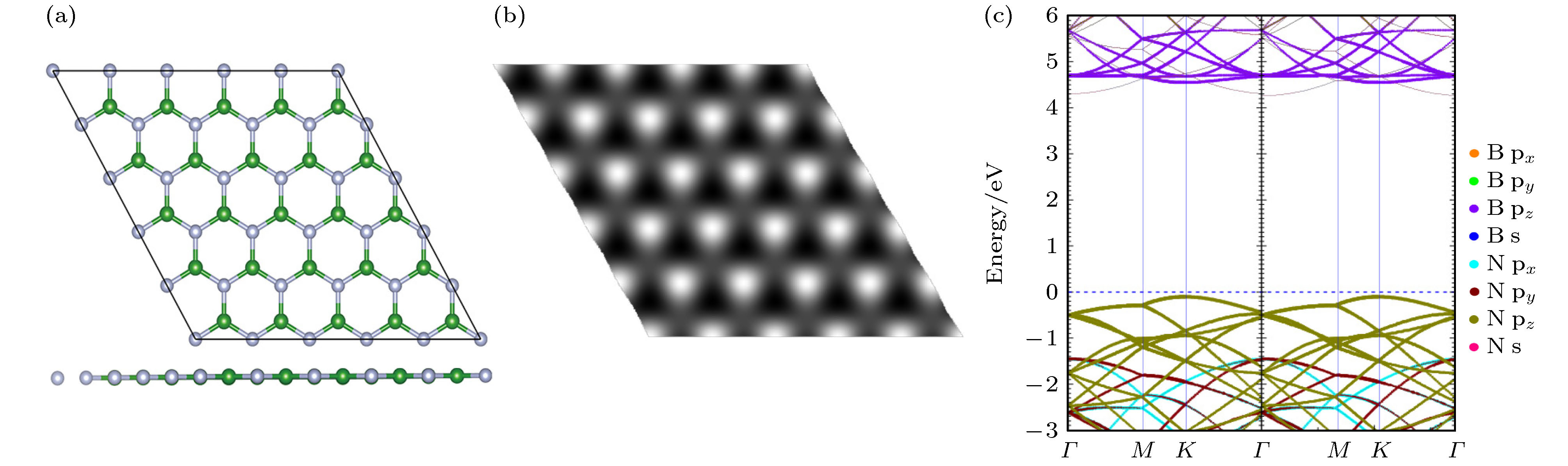
图 1 本征hBN单层 (a) hBN的俯视图和侧视图; (b) 模拟的hBN单层表面STM形貌, 加载电压为–2 V, 探针与原子表面的距离为0.479564 nm; (c) hBN的能带投影图
Fig. 1. Intrinsic hBN monolayer: (a) Top view and side view of hBN; (b) the simulated hBN single-layer surface STM morphology, loading voltage is –2 V, the distance between probe and atomic surface is 0.479564 nm; (c) energy band projection view of hBN.
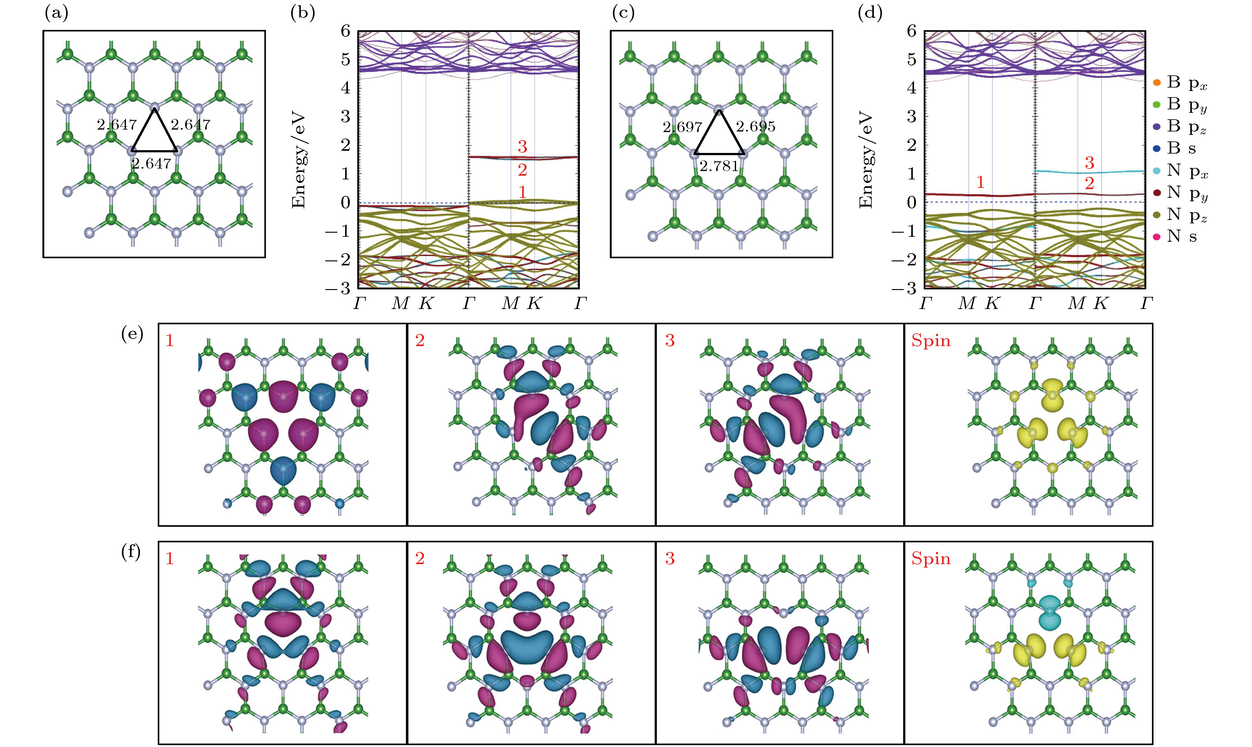
图 2 VB和as-VB的电子结构 (a), (c)分别为VB和as-VB优化后的局部结构俯视图; (b), (d)分别为VB和as-VB的能带投影图; (e), (f)分别为VB和as-VB的缺陷能级在Γ点处波函数的俯视图和自旋电荷密度图
Fig. 2. Electronic structure of VB and as-VB: (a), (c) The top views of the optimized partial structure of VB and as-VB, respectively; (b), (d) the energy band projection diagrams of VB and as-VB, respectively; (e), (f) the top view of the Γ-point wave functions of the defect levels and spin charge density of VB and as-VB, respectively.
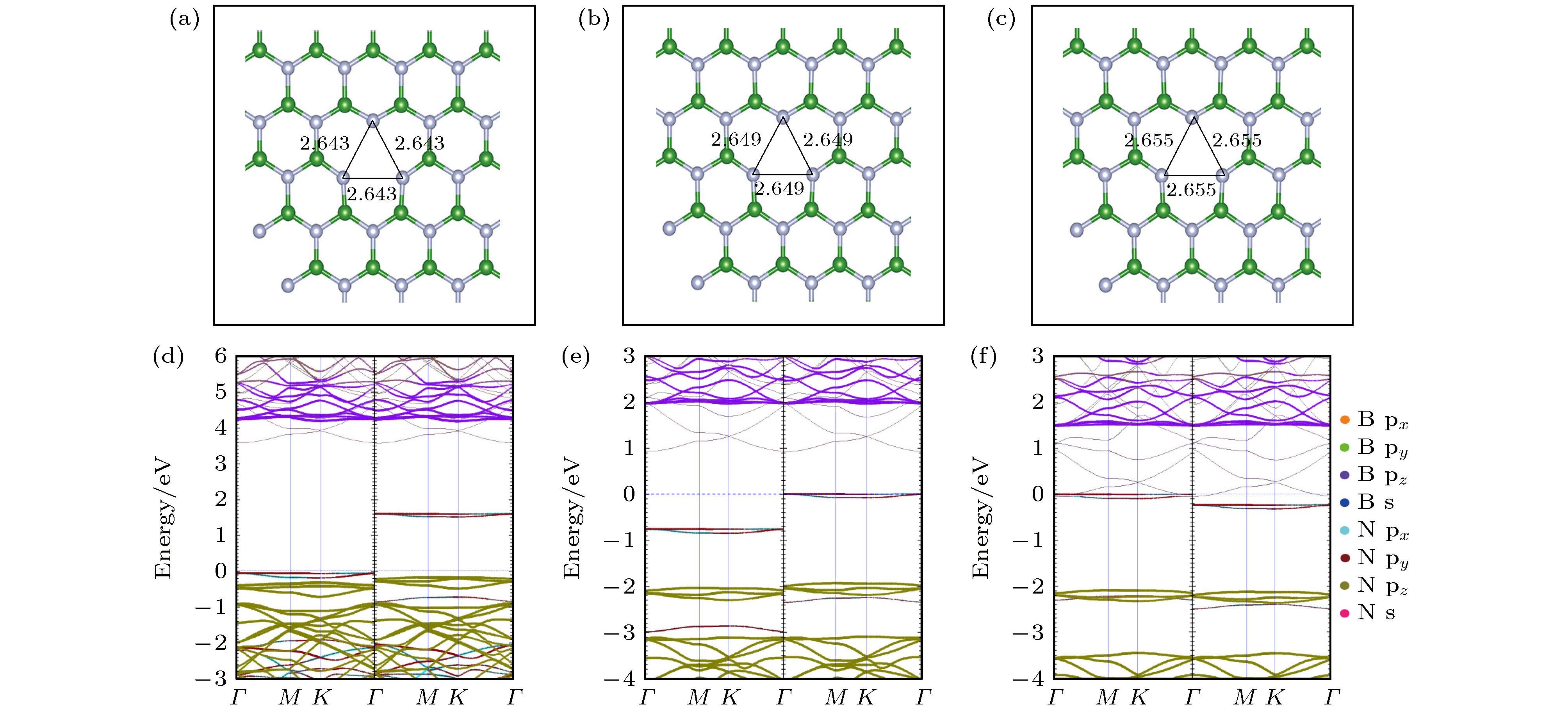
图 3 VB在不同价态的电子结构图 (a)−(c)分别为
$ {\rm{V}}_{\rm{B}}^{-1} $ ,$ {\rm{V}}_{\rm{B}}^{-2} $ ,$ {\rm{V}}_{\rm{B}}^{-3} $ 优化后的局部结构俯视图; (d)−(f)分别为$ {\rm{V}}_{\rm{B}}^{-1} $ ,$ {\rm{V}}_{\rm{B}}^{-2} $ ,${\rm{V}}_{\rm{B}}^{-3}$ 的能带投影图Fig. 3. Electronic structure diagrams of VB in different valence states: (a)−(c) The top views of the optimized partial structure diagrams of
$ {\rm{V}}_{\rm{B}}^{-1} $ ,$ {\rm{V}}_{\rm{B}}^{-2} $ , and$ {\rm{V}}_{\rm{B}}^{-3} $ , respectively; (d)−(f) the energy band projection diagrams of$ {\rm{V}}_{\rm{B}}^{-1} $ ,$ {\rm{V}}_{\rm{B}}^{-2} $ , and$ {\rm{V}}_{\rm{B}}^{-3} $ , respectively.
图 4 在富氮和贫氮条件下, 不同价态的VB形成能为费米能级的函数
Fig. 4. Formation energies of VB with different valences as a function of Fermi level under the nitrogen-rich and nitrogen-poor conditions.
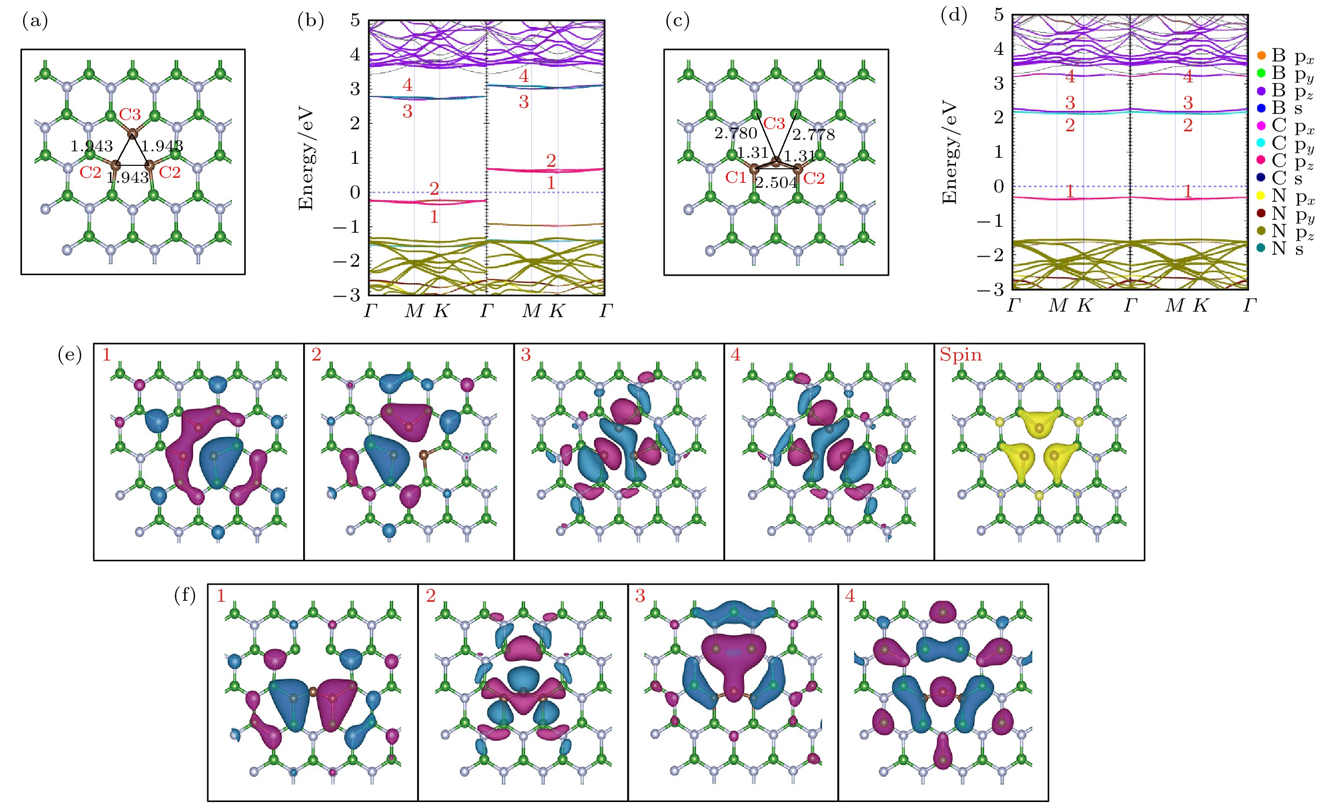
图 5 (CN)3VB和as-(CN)3VB的电子结构 (a), (c)分别为(CN)3VB, as-(CN)3VB优化后局部结构的俯视图; (b), (d)分别为(CN)3VB, as-(CN)3VB的能带投影图; (e) (CN)3VB缺陷能级在Γ点处的波函数图和自旋电荷密度图; (f) as-(CN)3VB缺陷能级在Γ点处的波函数图
Fig. 5. Electronic structure of (CN)3VB and as-(CN)3VB: (a), (c) The top views of the optimized partial structure of (CN)3VB and as-(CN)3VB; (b), (d) the energy band projection diagrams of (CN)3VB and as-(CN)3VB; (e) the top view of the Γ-point wave functions of the defect levels and spin charge density of (CN)3VB; (f) the top view of the Γ-point wave functions of the defect levels of as-(CN)3VB.
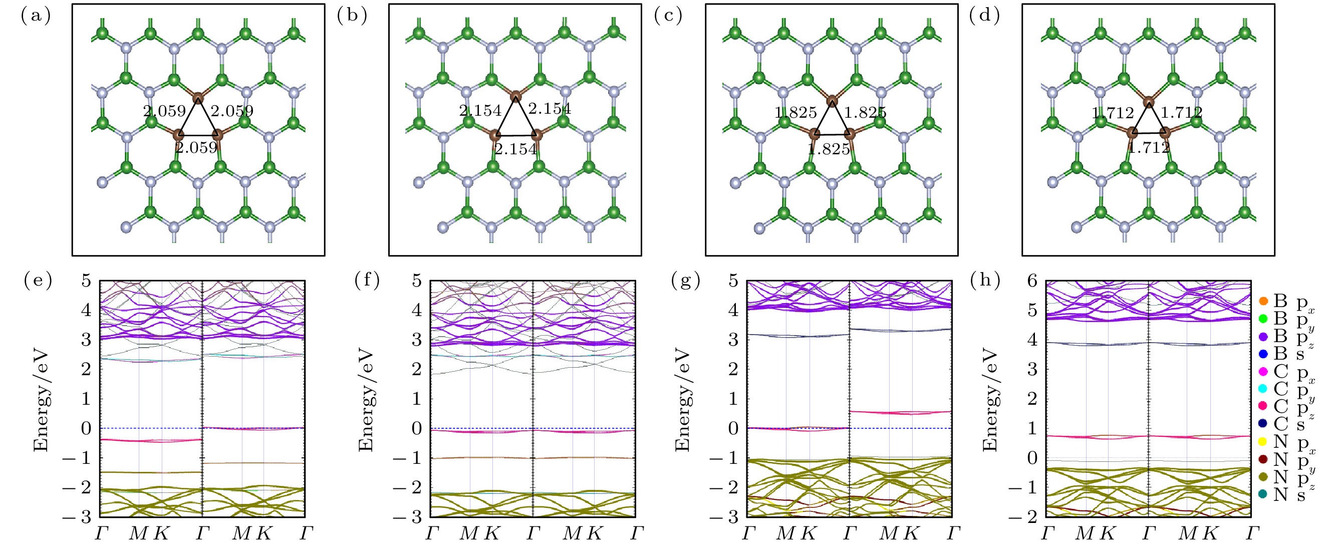
图 6 (CN)3VB不同价态优化后的局部结构和能带投影图 (a)−(d)分别为(CN)3
$ {\rm{V}}_{\rm{B}}^{-1} $ , (CN)3$ {\rm{V}}_{\rm{B}}^{-2} $ , (CN)3$ {\rm{V}}_{\rm{B}}^{+1} $ , (CN)3$ {\rm{V}}_{\rm{B}}^{+2} $ 优化后的局部结构图; (e)−(h)分别为(CN)3$ {\rm{V}}_{\rm{B}}^{-1} $ , (CN)3$ {\rm{V}}_{\rm{B}}^{-2} $ , (CN)3$ {\rm{V}}_{\rm{B}}^{+1} $ , (CN)3$ {\rm{V}}_{\rm{B}}^{+2} $ 的能带投影图Fig. 6. Local structure and energy band projection diagram of (CN)3VB after optimization of different valence states: (a)−(d) The top views of the optimized partial structure diagrams of (CN)3
$ {\rm{V}}_{\rm{B}}^{-1} $ , (CN)3$ {\rm{V}}_{\rm{B}}^{-2} $ , (CN)3$ {\rm{V}}_{\rm{B}}^{+1} $ , (CN)3$ {\rm{V}}_{\rm{B}}^{+2} $ ; (e)−(h) the energy band projection diagrams of (CN)3$ {\rm{V}}_{\rm{B}}^{-1} $ , (CN)3$ {\rm{V}}_{\rm{B}}^{-2} $ , (CN)3$ {\rm{V}}_{\rm{B}}^{+1} $ , (CN)3$ {\rm{V}}_{\rm{B}}^{+2} $ .
图 7 as-(CN)3VB不同价态优化后的局部结构和能带投影图 (a)−(d)分别为as-(CN)3
$ {\rm{V}}_{\rm{B}}^{-1} $ , as-(CN)3$ {\rm{V}}_{\rm{B}}^{-2} $ , as-(CN)3$ {\rm{V}}_{\rm{B}}^{+1} $ , as-(CN)3$ {\rm{V}}_{\rm{B}}^{+2} $ 优化后的局部结构图; (e)−(h)分别为as-(CN)3$ {\rm{V}}_{\rm{B}}^{-1} $ , as-(CN)3$ {\rm{V}}_{\rm{B}}^{-2} $ , as-(CN)3$ {\rm{V}}_{\rm{B}}^{+1} $ , as-(CN)3$ {\rm{V}}_{\rm{B}}^{+2} $ 的能带投影图Fig. 7. Electronic structure diagrams of as-(CN)3VB in different valence states: (a)−(d) The top views of the optimized partial structure diagrams of as-(CN)3
$ {\rm{V}}_{\rm{B}}^{-1} $ , as-(CN)3$ {\rm{V}}_{\rm{B}}^{-2} $ , as-(CN)3$ {\rm{V}}_{\rm{B}}^{+1} $ , as-(CN)3$ {\rm{V}}_{\rm{B}}^{+2} $ ; (e)−(h) the energy band projection diagrams of as-(CN)3$ {\rm{V}}_{\rm{B}}^{-1} $ , as-(CN)3$ {\rm{V}}_{\rm{B}}^{-2} $ , as-(CN)3$ {\rm{V}}_{\rm{B}}^{+1} $ , as-(CN)3$ {\rm{V}}_{\rm{B}}^{+2} $ .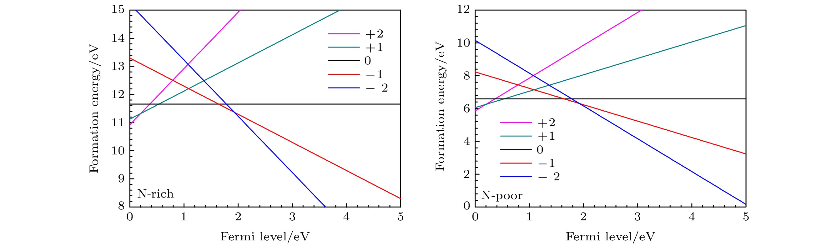
图 8 在富氮和贫氮条件下, 不同价态的(CN)3VB形成能为费米能级的函数
Fig. 8. Formation energies of (CN)3VB with different valences as a function of Fermi level under the nitrogen-rich and nitrogen-poor conditions.
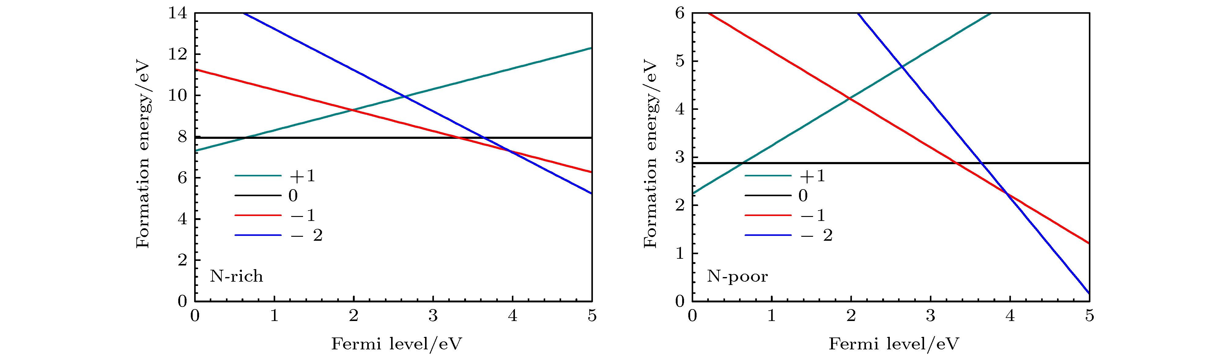
图 9 在富氮和贫氮条件下, 不同价态的as-(CN)3VB形成能为费米能级的函数
Fig. 9. Formation energies of as-(CN)3VB with different valences as a function of Fermi level under the nitrogen-rich and nitrogen-poor conditions.
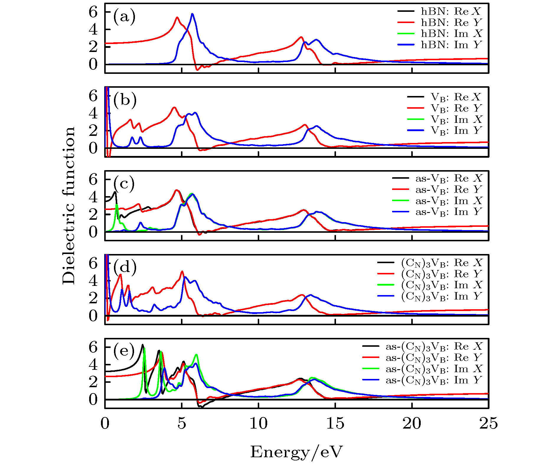
图 10 0 K和0 GPa时hBN, VB, as-VB, (CN)3VB, as-(CN)3VB的复介电函数
Fig. 10. Complex dielectric functions of hBN, VB, as-VB, (CN)3VB, as-(CN)3VB at 0 K and 0 GPa.
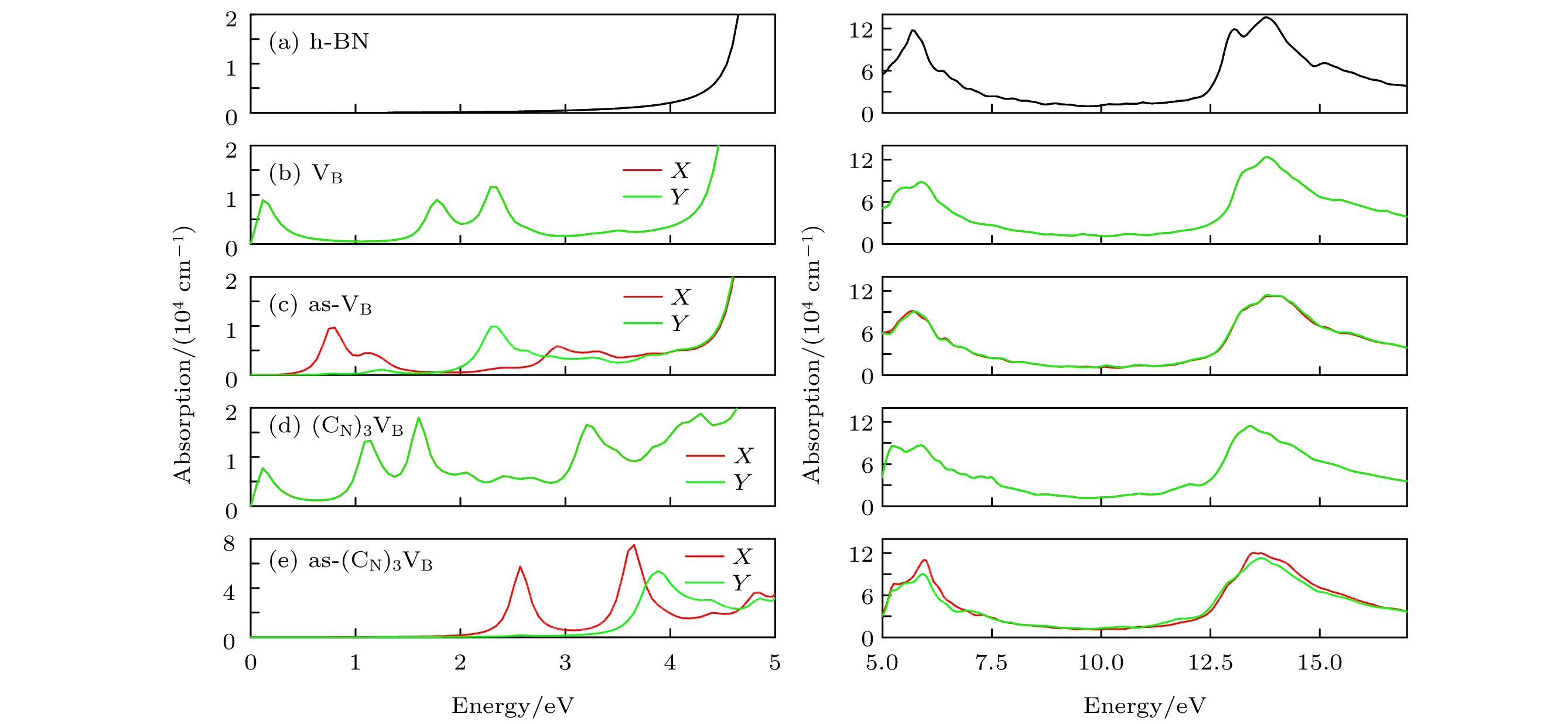
图 11 0 K和0 GPa时hBN, VB, as-VB, (CN)3VB, as-(CN)3VB的吸收系数
Fig. 11. Absorption coefficients of hBN, VB, as-VB, (CN)3VB, as-(CN)3VB at 0 K and 0 GPa.

图 12 0 K和0 GPa时hBN, VB, as-VB, (CN)3VB, as-(CN)3VB的损失函数
Fig. 12. Loss function of hBN, VB, as-VB, (CN)3VB, as-(CN)3VB at 0 K and 0 GPa.
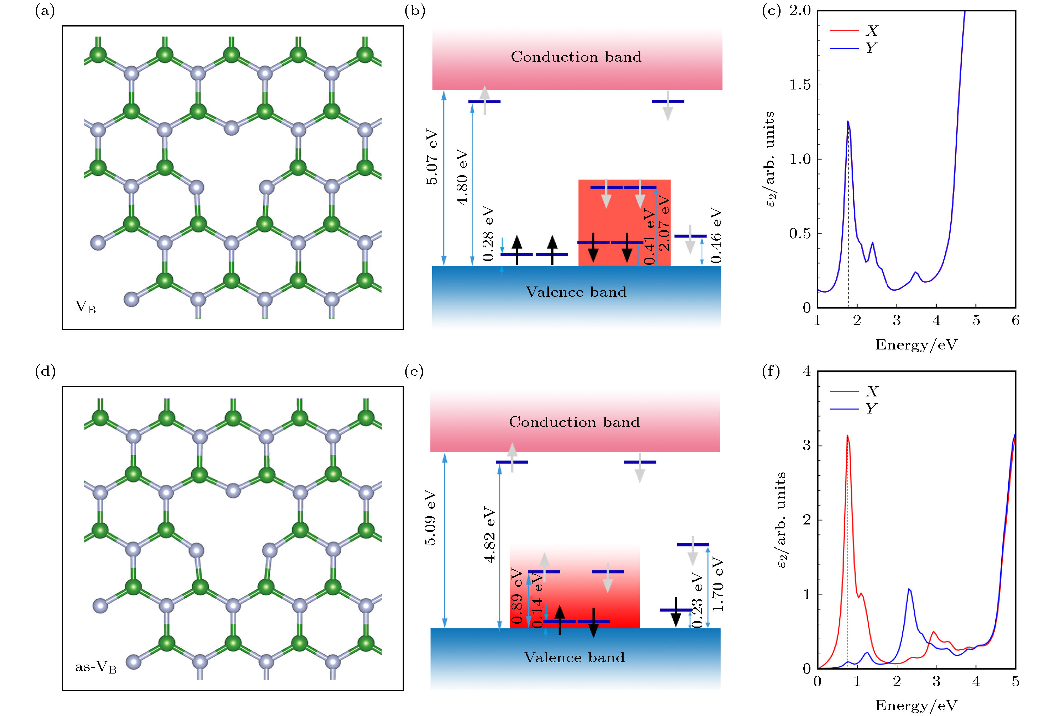
图 13 hBN单层硼原子空位的模型图 (a), (d)分别为VB和as-VB优化后的局部结构图; (b), (e)分别为VB和as-VB的电子结构模拟图, 黑色箭头和灰色箭头分别代表占据态和未占据态; (c), (f)分别为VB和as-VB的介电虚部在X和Y方向张量
Fig. 13. Model diagram of boron vacancies in hBN monolayer: (a), (d) The optimized local structure diagrams of VB and as-VB; (b), (e) simulated electronic structures diagrams of VB and as-VB, where black and grey arrows indicate occupied and unoccupied states; (c), (f) the tensors of the dielectric imaginary part of VB and as-VB in the X and Y directions.

图 14 hBN单层碳掺杂的模型图 (a), (d) (CN)3VB和as-(CN)3VB优化后的局部结构图; (b), (e) (CN)3VB和as-(CN)3VB的电子结构模拟图, 黑色箭头和灰色箭头分别代表占据态和未占据态; (c), (f) (CN)3VB和as-(CN)3VB的介电虚部在X和Y方向张量
Fig. 14. Model diagram of carbon doping in hBN monolayer: (a), (d) The optimized local structure diagrams of (CN)3VB and as-(CN)3VB; (b), (e) simulated electronic structures diagrams of (CN)3VB and as-(CN)3VB, where black and grey arrows indicate occupied and unoccupied states; (c), (f) the tensors of the dielectric imaginary part of (CN)3VB and as-(CN)3VB in the X and Y directions.
-
[1] Lee S, Yeo J S, Ji Y, Cho C, Kim D Y, Na S I, Lee B H, Lee T 2012 Nanotechnology 23 344013
Google Scholar
[2] Abderrahmane A, Ko P J, Thu T V, Ishizawa S, Takamura T, Sandhu A 2014 Nanotechnology 25 365202
Google Scholar
[3] Li X, Yin J, Zhou J, Wang Q, Guo W 2014 Nanotechnology 25 105701
Google Scholar
[4] Abdi M, Degenfeld-Schonburg P, Sameti M, Navarrete-Benlloch C, Hartmann M J 2016 Phys. Rev. Lett. 116 233604
Google Scholar
[5] Xia F, Wang H, Xiao D, Dubey M, Ramasubramaniam A 2014 Nat. Photonics 8 899
Google Scholar
[6] Clark G, Schaibley J R, Ross J, Taniguchi T, Watanabe K, Hendrickson J R, Mou S, Yao W, Xu X 2016 Nano Lett. 16 3944
Google Scholar
[7] Shiue R J, Efetov D K, Grosso G, Peng C, Fong K C, Englund D 2017 Nanophotonics 6 1329
Google Scholar
[8] Koenderink A F, Alu A, Polman A 2015 Science 348 516
Google Scholar
[9] Caldwell J D, Aharonovich I, Cassabois G, Edgar J H, Gil B, Basov D 2019 Nat. Rev. Mater. 4 552
Google Scholar
[10] Cai J, Retzker A, Jelezko F, Plenio M B 2013 Nat. Phys. 9 168
Google Scholar
[11] Pla J J, Tan K Y, Dehollain J P, Lim W H, Morton J J, Jamieson D N, Dzurak A S, Morello A 2012 Nature 489 541
Google Scholar
[12] Scarani V, Bechmann-Pasquinucci H, Cerf N J, Dušek M, Lütkenhaus N, Peev M 2009 Rev. Mod. Phys. 81 1301
Google Scholar
[13] O’brien J L, Furusawa A, Vučković J 2009 Nat. Photonics 3 687
Google Scholar
[14] Lo H K, Curty M, Tamaki K 2014 Nat. Photonics 8 595
Google Scholar
[15] Cheung J, Chunnilall C, Woolliams E, Fox N, Mountford J, Wang J, Thomas P 2007 J. Mod. Opt. 54 373
Google Scholar
[16] Rose B C, Huang D, Zhang Z H, Stevenson P, Tyryshkin A M, Sangtawesin S, Srinivasan S, Loudin L, Markham M L, Edmonds A M, Twitchen D J, Lyon S A, de Leon N P 2018 Science 361 60
Google Scholar
[17] Chen D, Zheludev N, Gao W B 2020 Adv. Quantum Technol. 3 1900069
Google Scholar
[18] Bradac C, Gao W, Forneris J, Trusheim M E, Aharonovich I 2019 Nat. Commun. 10 5625
Google Scholar
[19] Tran T T, Bray K, Ford M J, Toth M, Aharonovich I 2015 Nat. Nanotechnol. 11 37
Google Scholar
[20] Chakraborty C, Kinnischtzke L, Goodfellow K M, Beams R, Vamivakas A N 2015 Nat. Nanotechnol. 10 507
Google Scholar
[21] He Y M, Clark G, Schaibley J R, He Y, Chen M C, Wei Y J, Ding X, Zhang Q, Yao W, Xu X 2015 Nat. Nanotechnol. 10 497
Google Scholar
[22] Koperski M, Nogajewski K, Arora A, Cherkez V, Mallet P, Veuillen J Y, Marcus J, Kossacki P, Potemski M 2015 Nat. Nanotechnol. 10 503
Google Scholar
[23] Kumar S, Kaczmarczyk A, Gerardot B D 2015 Nano Lett. 15 7567
Google Scholar
[24] Srivastava A, Sidler M, Allain A V, Lembke D S, Kis A, Imamoglu A 2015 Nat. Nanotechnol. 10 491
Google Scholar
[25] Tonndorf P, Schmidt R, Schneider R, Kern J, Buscema M, Steele G A, Castellanos-Gomez A, van der Zant H S, Vasconcellos S M, Bratschitsch R 2015 Optica 2 347
Google Scholar
[26] Kern J, Niehues I, Tonndorf P, Schmidt R, Wigger D, Schneider R, Stiehm T, de Vasconcellos M S, Reiter D E, Kuhn T, Bratschitsch R 2016 Adv. Mater. 28 7101
Google Scholar
[27] Liu X, Hersam M C 2019 Nat. Rev. Mater. 4 669
Google Scholar
[28] Chen X, Lu X, Dubey S, Yao Q, Liu S, Wang X, Xiong Q, Zhang L, Srivastava A 2019 Nat. Phys. 15 221
Google Scholar
[29] Ziegler J, Klaiss R, Blaikie A, Miller D, Horowitz V R, Alemán B J 2019 Nano Lett. 19 2121
Google Scholar
[30] Chejanovsky N, Kim Y, Zappe A, Stuhlhofer B, Taniguchi T, Watanabe K, Dasari D, Finkler A, Smet J H, Wrachtrup J 2017 Sci. Rep. 7 14758
Google Scholar
[31] Jungwirth N R, Calderon B, Ji Y, Spencer M G, Flatte M E, Fuchs G D 2016 Nano Lett. 16 6052
Google Scholar
[32] Tran T T, Elbadawi C, Totonjian D, Lobo C J, Grosso G, Moon H, Englund D R, Ford M J, Aharonovich I, Toth M 2016 ACS Nano 10 7331
Google Scholar
[33] Dietrich A, Burk M, Steiger E S, Antoniuk L, Tran T T, Nguyen M, Aharonovich I, Jelezko F, Kubanek A 2018 Phys. Rev. B 98 081414
Google Scholar
[34] Meyer J C, Chuvilin A, Algara-Siller G, Biskupek J, Kaiser U 2009 Nano Lett. 9 2683
Google Scholar
[35] Alem N, Erni R, Kisielowski C, Rossell M D, Gannett W, Zettl A 2009 Phys. Rev. B 80 155425
Google Scholar
[36] Watanabe K, Taniguchi T, Kanda H 2004 Nat. Mater. 3 404
Google Scholar
[37] Kubota Y, Watanabe K, Tsuda O, Taniguchi T 2007 Science 317 932
Google Scholar
[38] Silly M, Jaffrennou P, Barjon J, Lauret J S, Ducastelle F, Loiseau A, Obraztsova E, Attal-Tretout B, Rosencher E 2007 Phys. Rev. B 75 085205
Google Scholar
[39] Museur L, Feldbach E, Kanaev A 2008 Phys. Rev. B 78 155204
Google Scholar
[40] Park H, Wadehra A, Wilkins J W, Castro Neto A H 2012 Appl. Phys. Lett. 100 253115
Google Scholar
[41] Weston L, Wickramaratne D, Mackoit M, Alkauskas A, van de Walle C G 2018 Phys. Rev. B 97 214104
Google Scholar
[42] Wang Y, Meng J, Tian Y, Chen Y, Wang G, Yin Z, Jin P, You J, Wu J, Zhang X 2020 ACS Appl. Mater. Interfaces 12 27361
Google Scholar
[43] Mendelson N, Chugh D, Reimers J R, Cheng T S, Gottscholl A, Long H, Mellor C J, Zettl A, Dyakonov V, Beton P H, Novikov S V, Jagadish C, Tan H H, Ford M J, Toth M, Bradac C, Aharonovich I 2020 Nat. Mater. DOI: 10.1038/s41563-020-00850-y
[44] Koperski M, Vaclavkova D, Watanabe K, Taniguchi T, Novoselov K S, Potemski M 2020 PNAS 117 13214
Google Scholar
[45] Kresse G, Kurthmuler J 1996 Comput. Mater. Sci. 6 15
Google Scholar
[46] Kresse G, Hafner J 1994 Phy. Rev. B 49 14251
Google Scholar
[47] Kresse G, Joubert D 1999 Phys. Rev. B 59 1758
Google Scholar
[48] Perdew J P, Burke K, Ernzerhof M 1996 Phys. Rev. Lett. 77 3865
Google Scholar
[49] Wei S H 2004 Comput. Mater. Sci. 30 337
Google Scholar
[50] Huang B, Lee H 2012 Phys. Rev. B 86 245406
Google Scholar
[51] Wickramaratne D, Shen J X, Dreyer C E, Alkauskas A, van de Walle C G 2019 Phys. Rev. B 99 205202
Google Scholar
[52] Shi Y, Hamsen C, Jia X, Kim K K, Reina A, Hofmann M, Hsu A L, Zhang K, Li H, Juang Z Y, Dresselhaus M S, Li L J, Kong J 2010 Nano Lett. 10 4134
Google Scholar
[53] Song L, Ci L, Lu H, Sorokin P B, Jin C, Ni J, Kvashnin A G, Kvashnin D G, Lou J, Yakobson B I, Ajayan P M 2010 Nano Lett. 10 3209
Google Scholar

 下载:
下载:


计量
- 文章访问数: 10937
- PDF下载量: 227
- 被引次数: 0
