


-
作为集成电路(ICs)的基础材料, 直拉硅(CZ-Si)单晶的机械强度不仅是硅片加工和ICs制造过程中工艺参数设定的重要考虑因素, 而且在很大程度上决定了ICs芯片在测试和封装过程中出现的失效情况. 目前, ICs的器件特征尺寸仍在继续减小, 由此带来的器件集成规模的增长会导致硅衬底中应力水平的提高, 从而使位错更易产生. 因此, 改善直拉硅片的机械强度对于提高ICs的制造成品率具有重要意义. 本文提出在直拉硅单晶中同时掺入锗和氮两种杂质来改善硅片机械强度的思路. 基于此, 对比研究了普通的、单一掺锗的、单一掺氮的、锗和氮共掺的直拉硅单晶的室温硬度及其在600—1200 ℃时的位错滑移行为. 研究结果表明: 1)单一的锗掺杂或氮掺杂以及锗和氮两种杂质的共掺几乎都不影响直拉硅单晶的室温硬度, 意味着上述掺杂没有改变室温下的位错滑移行为. 2)氮掺杂能显著抑制位错在600—1000 ℃的滑移, 但对位错在1100 ℃及以上温度的滑移几乎没有抑制效应; 锗掺杂几乎不能抑制位错在 600—900 ℃的滑移, 但对位错在1000 ℃及以上温度的滑移具有显著的抑制效应. 3)锗和氮两种杂质的共掺对位错在600—1200 ℃的滑移均有显著的抑制效应, 表明氮掺杂和锗掺杂的互补优势得到了很好的结合. 分析认为, 在600—1000 ℃的温度范围内, 氮掺杂导致在位错核心处形成与氮-氧复合体相关的钉扎中心, 从而抑制位错的滑移; 在1000 ℃及以上温度, 锗掺杂导致在位错前沿附近形成锗-氧复合体, 从而阻碍位错的滑移. 总之, 本文的研究表明在直拉硅单晶中同时掺入锗和氮两种杂质可以进一步地增强硅片在ICs制造工艺温度下的机械强度.Czochralski (CZ) silicon is a base material for manufacturing integrated circuits (ICs). The mechanical strength of CZ silicon determines the processing limitations and often dominates the issues related to packaging and failure of ICs. With the ever-smaller feature size of ICs, the scaling of device dimensions may indirectly lead to increase the stress in silicon substrate, thus increasing the probability of generating dislocations. Consequently, improving the mechanical strength of CZ silicon is of significance for increasing the manufacturing yield of ICs. In this work, we propose a strategy of co-doping germanium (Ge) impurity and nitrogen (N) impurity into CZ silicon to achieve better mechanical strength. In order to explore the feasibility of such a strategy, we comparatively investigate the room-temperature hardness and dislocation gliding behaviors in the temperature range of 600–1200 ℃ in the conventional CZ silicon, Ge-doped CZ silicon, N-doped CZ silicon, as well as N and Ge co-doped CZ silicon. The significant experimental results are described as follows. 1) Ge-doping, N-doping or co-doping of Ge and N hardly influences the hardness and therefore the dislocation gliding behavior at room temperature. 2) The suppressing effect of N-doping on the dislocation gliding is remarkable at 600–1000 ℃ and becomes weakened at the temperatures higher than 1100 ℃, while Ge-doping hardly affects the dislocation gliding at 600–900 ℃ but exhibits a strong suppressing effect on the dislocation gliding at 1000–1200 ℃. 3) Co-doping Ge and N impurities into CZ silicon can take the complementary advantages of both Ge- and N-doping to suppress the dislocation gliding at 600–1200 ℃. It is believed that N-doping can result in the formation of N-O complex-related pinning agents within the dislocation cores to suppress the dislocation gliding at 600–1000 ℃. For Ge-doping, it is supposed that Ge-O complexes acting as the pinning agents can form near the front of a single dislocation when the temperature is as high as 1000 ℃ and above. In a word, it is verified in this work that co-doping Ge and N into CZ silicon can further improve the mechanical strength at the processing temperatures of ICs fabrication.
-
Keywords:
- Czochralski slicon /
- mechanical strength /
- dislocation gliding /
- co-doping /
- germanium /
- nitrogen
[1] Hu S M, Patrick W J 1975 J. Appl. Phys. 46 1869
 Google Scholar
[2] Sumino K, Harada H, Yonenaga I 1980 Jpn. J. Appl. Phys. 19 L49
Google Scholar
[3] Yonenaga I, Sumino K, Hoshi K 1984 J. Appl. Phys. 56 2346
Google Scholar
[4] Senkader S, Wilshaw P R, Gambaro D, et al. 1999 Solid State Phenom. 70 321
Google Scholar
[5] Yang D R, Wang G, Xu J, et al. 2003 Microelectron. Eng. 66 345
Google Scholar
[6] Zeng Z D, Chen J H, Zeng Y H, et al. 2011 J. Cryst. Growth 324 93
Google Scholar
[7] Shimizu H, Aoshima T 1988 Jpn. J. Appl. Phys. 27 2315
Google Scholar
[8] Fischer A, Kissinger G 2007 Appl. Phys. Lett. 91 111911
Google Scholar
[9] Goldstein M, Watanabe M 2008 ECS Trans. 16 313
Google Scholar
[10] Fahey P M, Mader S R, Stiffler S R, et al. 1992 IBM J. Res. Dev. 36 158
Google Scholar
[11] Siegelin F, Stuffer A 2005 Proceedings of the 31st International Symposium for Testing and Failure Analysis San Jose, California, USA, November 6–10, 2005 p59
[12] Yonenaga I 2005 J. Appl. Phys. 98 023517
Google Scholar
[13] Lu H M, Yang D R, Li L B, et al. 1998 Phys. Status Solidi A 169 193
Google Scholar
[14] Li D S, Yang D R, Que D L 1999 Physica B 273-4 553
Google Scholar
[15] Orlov V, Richter H, Fischer A, et al. 2002 Mater. Sci. Semicond. Process. 5 403
Google Scholar
[16] Mezhennyi M V, Mil’vidskii M G, Reznik V Y 2002 Phys. Solid State 44 1278
Google Scholar
[17] Mezhennyi M V, Mil’vidskii M G, Reznik V Y 2009 J. Surf. Invest. 3 747
Google Scholar
[18] Fukuda T, Ohsawa A 1992 Appl. Phys. Lett. 60 1184
Google Scholar
[19] Yonenaga I 2005 Mater. Sci. Eng., B 124 293
Google Scholar
[20] Chen J H, Yang D R, Ma X Y, et al. 2008 J. Appl. Phys. 103 123521
Google Scholar
[21] Taishi T, Huang X M, Yonenaga I, et al. 2002 Mater. Sci. Semicond. Process. 5 409
Google Scholar
[22] Schuh C A 2006 Mater. Today 9 32
Google Scholar
[23] Jang J I, Lance M J, Wen S Q, et al. 2005 Acta Mater. 53 1759
Google Scholar
[24] Juliano T, Gogotsi Y, Domnich V 2003 J. Mater. Res. 18 1192
Google Scholar
[25] Sun Y, Zhao T, Lan W, et al. 2019 J. Mater. Sci.- Mater. Electron. 30 3114
Google Scholar
[26] Kailer A, Gogotsi Y G, Nickel K G 1997 J. Appl. Phys. 81 3057
Google Scholar
[27] Oliver W C, Pharr G M 1992 J. Mater. Res. 7 1564
Google Scholar
[28] Imai M, Sumino K 1983 Philos. Mag. A 47 599
Google Scholar
[29] Sumino K, Yonenaga I 1993 Phys. Status Solidi A 138 573
Google Scholar
[30] Kolar H R, Spence J C H, Alexander H 1996 Phys. Rev. Lett. 77 4031
Google Scholar
[31] Patel J R, Testardi L R, Freeland P E 1976 Phys. Rev. B 13 3548
Google Scholar
[32] Suzuki T, Yonenaga I, Kirchner H O K 1995 Phys. Rev. Lett. 75 3470
Google Scholar
[33] Yang D R, Ma X Y, Fan R X, et al. 2000 Mater. Sci. Eng., B 72 121
Google Scholar
[34] von Ammon W, Holzl R, Virbulis J, et al. 2002 J. Cryst. Growth 240 330
Google Scholar
[35] Ko ji, Sumino 1999 Metall. Mater. Trans. A 30 1465
Google Scholar
[36] Itoh T, Abe T 1988 Appl. Phys. Lett. 53 39
Google Scholar
[37] Yonenaga I, Taishi T, Huang X, et al. 2003 J. Appl. Phys. 93 265
Google Scholar
[38] Sumino K, Yonenaga I 2002 Solid State Phenom. 85-86 145
Google Scholar
[39] McVay G L, Ducharme A R 1973 J. Appl. Phys. 44 1409
Google Scholar
[40] Wang L, Yang D R 2009 Physica B 404 58
Google Scholar
-
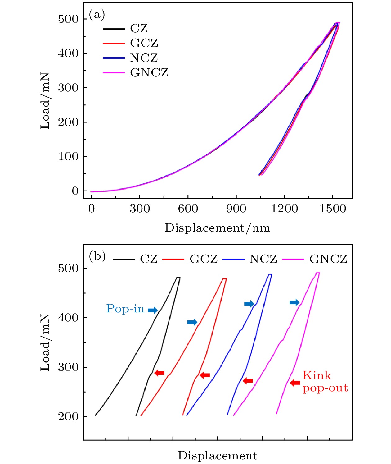
图 1 (a) CZ, GCZ, NCZ, GNCZ硅单晶样品的典型纳米压痕载荷-位移(P-h)曲线; (b)各样品带有相变特征的部分载荷-位移曲线(为了可视起见, 各曲线作了平移)
Fig. 1. (a) Representative P-h curves of CZ, GCZ, NCZ, GNCZ silicon specimens under nanoindentation; (b) segments of the P-h curves with features of phase transformation for CZ, GCZ, NCZ, GNCZ silicon specimens (the curves are deliberately shifted for visual discrimination).

图 2 CZ, GCZ, NCZ, GNCZ硅样品(a) 纳米压痕硬度和(b)维氏硬度的平均值及其标准差
Fig. 2. Average values and standard deviations of the (a) nanoindentation hardness and (b) Vikers hardness of CZ, GCZ, NCZ and GNCZ silicon specimens.

图 3 (a) 三点弯曲加载单元的结构示意图以及加载时的载荷-位置分布关系的示意图; (b) 普通CZ硅样品在650 ℃三点弯曲加载25 min并经择优腐蚀后某一部分区域的OM照片
Fig. 3. (a) Schematic diagram of three-point bending unit and the dependence of load on the position under a given loading; (b) regional OM image of the conventional CZ silicon specimen subjected to three-point bending at 650 ℃ for 25 min and subsequent preferential etching.
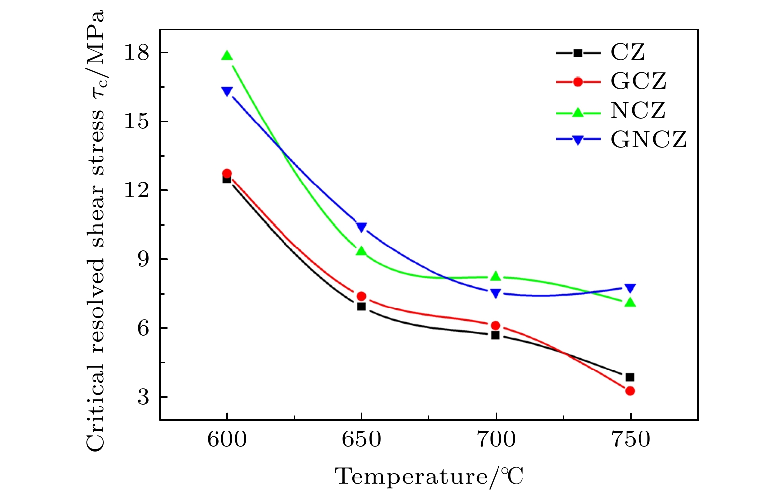
图 4 CZ, GCZ, NCZ, GNCZ样品在600−750 ℃位错滑移的临界切应力
Fig. 4. Critical shear stresses of dislocation gliding in CZ, GCZ, NCZ and GNCZ silicon specimens at temperature in the range of 600−750 ℃.

图 5 施加压痕的CZ, GCZ, NCZ, GNCZ样品经900−1200 ℃退火后得到的位错rosette尺寸的统计结果
Fig. 5. Statistical results for the dislocation rosette sizes in the indented CZ, GCZ, NCZ and GNCZ silicon specimens annealed at 900−1200 ℃
表 1 实验所采用的硅片中的杂质浓度
Table 1. Concentrations of impurities in the silicon wafers used.
硅片 杂质 [Ge]/(1019 cm–3) [N]/(1014 cm–3) [Oi]/(1017 cm–3) CZ — — 7.9 GCZ 2.8 — 8.1 NCZ — 9.0 8.1 GNCZ 2.0 8.1 8.0  下载: 导出CSV
表 2 CZ, NCZ, GCZ, GNCZ样品的位错滑移激活能
Table 2. Activation energy of dislocation gliding in CZ, NCZ, GCZ and GNCZ silicon specimens.
CZ GCZ NCZ GNCZ Q /eV 2.12 2.10 2.07 2.00
下载: 导出CSV
-
[1] Hu S M, Patrick W J 1975 J. Appl. Phys. 46 1869
Google Scholar
[2] Sumino K, Harada H, Yonenaga I 1980 Jpn. J. Appl. Phys. 19 L49
Google Scholar
[3] Yonenaga I, Sumino K, Hoshi K 1984 J. Appl. Phys. 56 2346
Google Scholar
[4] Senkader S, Wilshaw P R, Gambaro D, et al. 1999 Solid State Phenom. 70 321
Google Scholar
[5] Yang D R, Wang G, Xu J, et al. 2003 Microelectron. Eng. 66 345
Google Scholar
[6] Zeng Z D, Chen J H, Zeng Y H, et al. 2011 J. Cryst. Growth 324 93
Google Scholar
[7] Shimizu H, Aoshima T 1988 Jpn. J. Appl. Phys. 27 2315
Google Scholar
[8] Fischer A, Kissinger G 2007 Appl. Phys. Lett. 91 111911
Google Scholar
[9] Goldstein M, Watanabe M 2008 ECS Trans. 16 313
Google Scholar
[10] Fahey P M, Mader S R, Stiffler S R, et al. 1992 IBM J. Res. Dev. 36 158
Google Scholar
[11] Siegelin F, Stuffer A 2005 Proceedings of the 31st International Symposium for Testing and Failure Analysis San Jose, California, USA, November 6–10, 2005 p59
[12] Yonenaga I 2005 J. Appl. Phys. 98 023517
Google Scholar
[13] Lu H M, Yang D R, Li L B, et al. 1998 Phys. Status Solidi A 169 193
Google Scholar
[14] Li D S, Yang D R, Que D L 1999 Physica B 273-4 553
Google Scholar
[15] Orlov V, Richter H, Fischer A, et al. 2002 Mater. Sci. Semicond. Process. 5 403
Google Scholar
[16] Mezhennyi M V, Mil’vidskii M G, Reznik V Y 2002 Phys. Solid State 44 1278
Google Scholar
[17] Mezhennyi M V, Mil’vidskii M G, Reznik V Y 2009 J. Surf. Invest. 3 747
Google Scholar
[18] Fukuda T, Ohsawa A 1992 Appl. Phys. Lett. 60 1184
Google Scholar
[19] Yonenaga I 2005 Mater. Sci. Eng., B 124 293
Google Scholar
[20] Chen J H, Yang D R, Ma X Y, et al. 2008 J. Appl. Phys. 103 123521
Google Scholar
[21] Taishi T, Huang X M, Yonenaga I, et al. 2002 Mater. Sci. Semicond. Process. 5 409
Google Scholar
[22] Schuh C A 2006 Mater. Today 9 32
Google Scholar
[23] Jang J I, Lance M J, Wen S Q, et al. 2005 Acta Mater. 53 1759
Google Scholar
[24] Juliano T, Gogotsi Y, Domnich V 2003 J. Mater. Res. 18 1192
Google Scholar
[25] Sun Y, Zhao T, Lan W, et al. 2019 J. Mater. Sci.- Mater. Electron. 30 3114
Google Scholar
[26] Kailer A, Gogotsi Y G, Nickel K G 1997 J. Appl. Phys. 81 3057
Google Scholar
[27] Oliver W C, Pharr G M 1992 J. Mater. Res. 7 1564
Google Scholar
[28] Imai M, Sumino K 1983 Philos. Mag. A 47 599
Google Scholar
[29] Sumino K, Yonenaga I 1993 Phys. Status Solidi A 138 573
Google Scholar
[30] Kolar H R, Spence J C H, Alexander H 1996 Phys. Rev. Lett. 77 4031
Google Scholar
[31] Patel J R, Testardi L R, Freeland P E 1976 Phys. Rev. B 13 3548
Google Scholar
[32] Suzuki T, Yonenaga I, Kirchner H O K 1995 Phys. Rev. Lett. 75 3470
Google Scholar
[33] Yang D R, Ma X Y, Fan R X, et al. 2000 Mater. Sci. Eng., B 72 121
Google Scholar
[34] von Ammon W, Holzl R, Virbulis J, et al. 2002 J. Cryst. Growth 240 330
Google Scholar
[35] Ko ji, Sumino 1999 Metall. Mater. Trans. A 30 1465
Google Scholar
[36] Itoh T, Abe T 1988 Appl. Phys. Lett. 53 39
Google Scholar
[37] Yonenaga I, Taishi T, Huang X, et al. 2003 J. Appl. Phys. 93 265
Google Scholar
[38] Sumino K, Yonenaga I 2002 Solid State Phenom. 85-86 145
Google Scholar
[39] McVay G L, Ducharme A R 1973 J. Appl. Phys. 44 1409
Google Scholar
[40] Wang L, Yang D R 2009 Physica B 404 58
Google Scholar

 下载:
下载:
计量
- 文章访问数: 10563
- PDF下载量: 154
- 被引次数: 0
