


-
GaInAsSb quaternary alloys have attracted much interest in infrared optoelectronic applications due to their versatility in a large range of energy gaps from 0.296 eV to 0.726 eV when lattice matches to GaSb wafer. However, due to the high intrinsic carrier concentration and Auger recombination, GaInAsSb p-n junctions typically are characterized by high dark current density at room temperature and need to be operated at low temperature to obtain high optoelectronic performance. In this work, a front surface wide-bandgap semiconductor nano pillar array (NPA) and a high reflective metal back surface reflector (BSR) are designed to modulate optoelectronic performances of GaInAsSb p-n junction. The optical and optoelectronic characteristics are analyzed by the finite difference time domain simulation and the numerical solution of carrier transport equations, respectively. It shows that the NPA-BSR structure can trigger Mie-type resonance, Wood-Rayleigh anomaly effect and Fabry-Perot resonance, which can be used to trap the light efficiently in an ultrathin GaInAsSb film. Owing to these nanophotonic effects, the average light absorption of ~90% can be obtained in 1.0–2.3 μm infrared waveband for 1μm Ga0.84In0.16As0.14Sb0.86. It also shows that the Auger recombination can be suppressed with thickness decreasing which leads the carrier collection efficiency to increase and the dark current density to decrease. Theoretical results show that the carrier collection efficiency of ~99% and dark current density of ~5×10⁻⁶ A/cm2 can be obtained for the 1 μm Ga0.84In0.16As0.14Sb0.86 p-n junction. With these unique optoelectronic properties, the NPA-BSR nanophotonic structure can become a very promising method to realize the high performance ultrathin GaInAsSb infrared optoelectronic devices.
-
Keywords:
- nanophotonic /
- GaInAsSb /
- infrared
[1] 刘超 魏志鹏 安宁 何斌太 刘鹏程 刘国军 2014 物理学报 63 248102
 Google Scholar
Liu C, Wei Z P, An N, He B T, Liu P C, Liu G J 2014 Acta Phys. Sin. 63 248102
Google Scholar
[2] Mitsuhara M, Ohiso Y, Matsuzaki H 2020 J. Cryst. Growth 535 125551
Google Scholar
[3] Hao H Y, Wang G W, Han X, Jiang D W, Sun, Y Y, Guo C Y, Xiang W, Xu Y Q and Niu Z C 2018 AIP Adv. 8 095106
Google Scholar
[4] Lou Y Y, Zhang X L, Huang A B, Wang Y 2018 Sol. Energ. Mat. Sol. C. 172 124
[5] Liu Q, Marshall A, Kirer A 2019 Materials (Basel) 12 1743
Google Scholar
[6] Wang Y, Lou Y Y 2015 Renew. Energ. 75 8
Google Scholar
[7] You M H, Sun Q X, Yin L P, Fan J J, Liang X M, Li X, Yu X L, Li S J, Liu J S 2016 J. Nanomater. 2016 393502
[8] Liang B L, Chen D Y, Wang B, Kwasniewski T A, Wang Z G 2010 IEEE T. Electron Dev. 57 361
Google Scholar
[9] Rothmayr F, Pfenning A, Kistner C, Koeth J, Knebl G, Schade A, Krueger S, Worschech L, Hartmann F, Höfling S 2018 Appl. Phys. Lett. 112 161107
Google Scholar
[10] Peng X C, Guo X, Zhang B L, Li X P, Zhao X W, Dong X, Zheng W, Du G T 2010 Infrared Phys. Techn. 53 37
Google Scholar
[11] 秦飞飞 张海明 王彩霞 郭聪 张晶晶 2014 物理学报 63 198802
Google Scholar
Qin F F, Zhang H M, Wang C X, Guo C, Zhang J J 2014 Acta Phys. Sin. 63 198802
Google Scholar
[12] El-Batawy Y M, Deen M J 2003 Proc. SPIE 4999 363
Google Scholar
[13] Jiang A Q, Osamu Y, Chen L Y 2020 SCI REP-UK 10 12780
Google Scholar
[14] Chen H L, Cattoni A, Lépinau R D, Walker A W, Höhn O, Lackner D, Siefer G, Faustini M, Vandamme N, Goffard J, Behaghel B, Dupuis C, Bardou N, Dimroth F, Collin S 2019 Nat. energy 4 761
Google Scholar
[15] Amalathas A P, Alkaisi M M 2019 Micromachines 10 619
Google Scholar
[16] Proise F, Joudrier A, Pardo F, Pelouard J, Guillemoles J 2018 Opt. Express 26 A806
Google Scholar
[17] Yang Z H, Gao P Q, Zhang C, Li X F, Ye J C 2016 SCI REP-UK 6 30503
Google Scholar
[18] Kuznetsov A I, Miroshnichenko A E, Brongersma M L, Kivshar Y S, Luk’yanchuk B 2016 Science 354 aag2472
Google Scholar
[19] Jahani S, Jacob Z 2016 Nat. Nanotechnol. 11 23
Google Scholar
[20] Behaghel B, Tamaki R, Vandamme N, Watanabe K, Dupuis C, Bardou N, Sodabanlu H, Cattoni A, Okada Y, Sugiyama M, Collin S, Guillemoles J 2015 Appl. Phys. Lett. 106 081107
Google Scholar
[21] Peng X C, Wang Z D, Liu Y, Manos D M, Poelker M, Stutzman M, Tang B, Zhang S K, Zou J J 2019 Phys. Rev. Appl. 12 064002
Google Scholar
[22] 彭新村, 王智栋, 曾梦丝, 刘云, 邹继军, 朱志甫, 邓文娟 2019 无机材料学报 34 734
Google Scholar
Peng X C, Wang Z D, Zeng M S, Liu Y, Zou J J, Zhu Z F, Deng W J 2019 J. Inorg. Mater. 34 734
Google Scholar
[23] Wang C A, Shiau D A, Murphy P G, O'Brien P W, Huang R K, Connors M K, Anderson A C, Donetsky D, Anikeev S, Belenky G, Depoy D M, Nichols G 2004 J. Electron. Mater. 33 213
Google Scholar
[24] 彭新村 王智栋 邓文娟 朱志甫 邹继军 张益军 2020 物理学报 69 068501
Google Scholar
Peng X C, Wang Z D, Deng W J, Zhu Z F, Zou J J, Zhang Y J 2020 Acta Phys. Sin. 69 068501
Google Scholar
[25] Tian Y, Chua S J, Jin Y X 2003 Microelectron. J. 34 304
[26] Peng X C, Poelker M, Stutzman M, Tang B, Zhang S K, Zou J J 2020 Opt. Express 28 860
Google Scholar
[27] Wang Y, Chen N F, Zhang X W, Huang T M, Yin Z G, Wang Y S, Zhang H 2010 Sol. Energ. Mat. Sol. C. 94 1704
Google Scholar
[28] Tang L L, Fraas L M, Liu Z M, Xu C, Chen X Y 2016 IEEE T. Electron Dev. 63 3591
Google Scholar
[29] Dashiell M W, Beausang J F, Ehsani H, Nichols G J, Depoy D M, Danielson L R, Talamo P, Rahner K D, Brown E J, Burger S R, Fourspring P M, Topper W F, Jr., Baldasaro P F, Wang C A, Huang R K, Connors M K, Turner G W, Shellenbarger Z A, Taylor G, Li J Z, Martinelli R, Donetski D, Anikeev S, Belenky G L, Luryi S 2006 IEEE T. Electron Dev. 53 2879
Google Scholar
[30] Groep J, Polman A 2013 Opt. Express 21 26285
Google Scholar
[31] Wang Z Y, Zhang R J, Wang S Y, Lu M, Chen X, Zheng Y X, Chen L Y, Ye Z, Wang C Z, Ho K M 2015 SCI REP-UK 5 7810
Google Scholar
[32] Wang C A 2004 AIP Conf. Proc. 738 255
Google Scholar
-
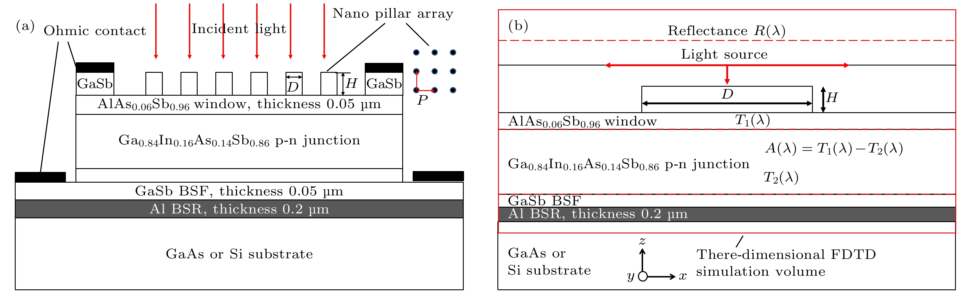
图 1 双面光调控Ga0.84In0.16As0.14Sb0.86 p-n结 (a)材料结构; (b)三维FDTD光学仿真设置
Figure 1. Illustration of the two-side light modulation structured Ga0.84In0.16As0.14Sb0.86 p-n junction: (a) Material structure; (b) cross-section of the three-dimensional FDTD optical simulation setup.
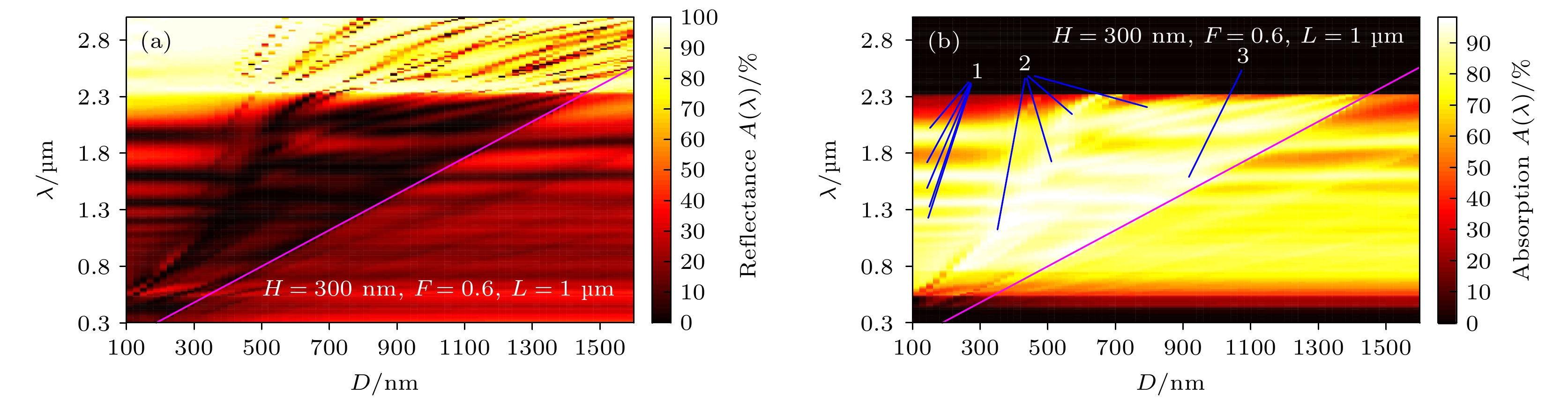
图 2 纳米柱直径D对Ga0.84In0.16As0.14Sb0.86 p-n结光学特性的影响 (a)表面反射谱; (b)有源区光吸收谱
Figure 2. Effects of the nanopillar diameter D on the optical properties of the Ga0.84In0.16As0.14Sb0.86 p-n junction: (a) Surface reflectance spectrum; (b) absorption spectrum in active region.

图 3 纳米柱填充因子F对Ga0.84In0.16As0.14Sb0.86 p-n结有源区的光吸收谱的影响
Figure 3. Effects of the nanopillar fill factor F on the absorption of the Ga0.84In0.16As0.14Sb0.86 p-n junction active region.
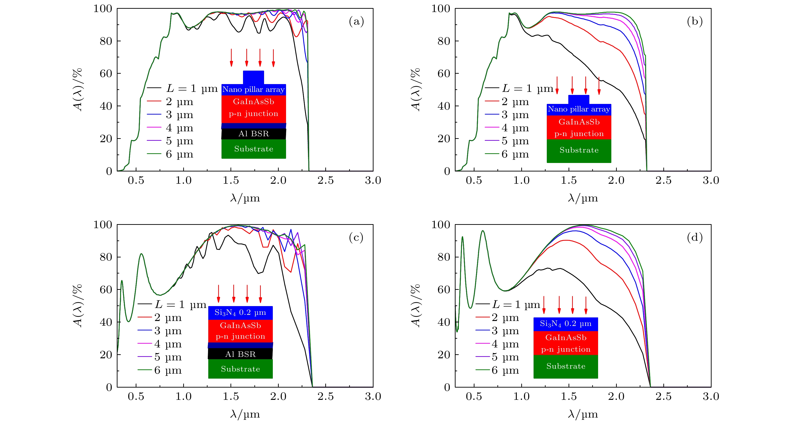
图 4 不同光学结构下Ga0.84In0.16As0.14Sb0.86 p-n结有源区的光吸收谱 (a)NPA和BSR双面光调控结构; (b)NPA单面光调控结构; (c)表面1/4波长Si3N4增透膜和BSR双面光调控结构; (d)表面1/4波长Si3N4增透膜单面光调控结构. 其中NPA尺寸为H = 300 nm, D = 540 nm, F = 0.6, Si3N4增透膜的中心波长设计为1.6 µm
Figure 4. Absorption spectrums of the Ga0.84In0.16As0.14Sb0.86 p-n junction active region under different optical structures: (a) NPA-BSR two-side light modulation structure; (b) NPA one-side light modulation structure; (c) surface λ/4 Si3N4 anti-reflection film and BSR two-side light modulation structure; (d) surface λ/4 Si3N4 anti-reflection film one-side light modulation structure. The NPA geometry parameters are set as H = 300 nm, D = 540 nm and F = 0.6, central wavelength of the λ/4 Si3N4 anti-reflection film is set as 1.6 µm.

图 5 室温(300 K)下Ga0.84In0.16As0.14Sb0.86 p-n结的IQE
Figure 5. IQE for Ga0.84In0.16As0.14Sb0.86 p-n junction diode at 300 K.
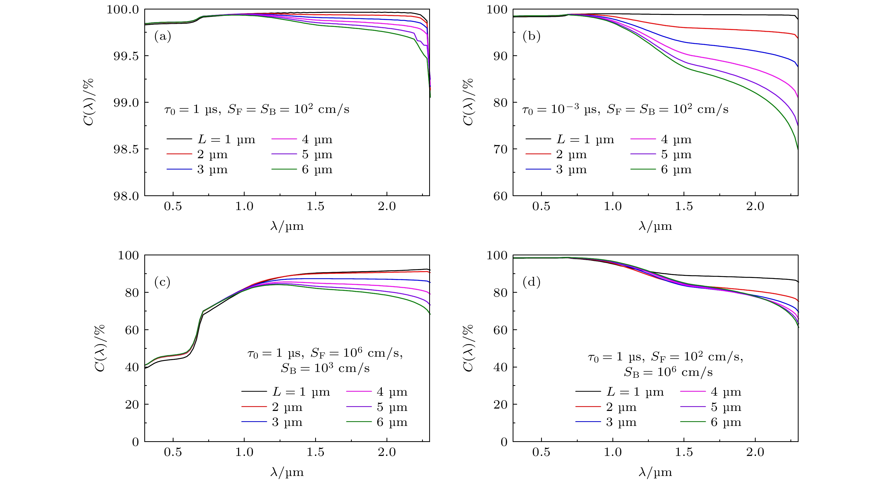
图 6 不同复合参数下载流子收集效率谱C(λ)随波长λ和有源区总厚度L的变化 (a) τ0 =1 µs, SF = SB = 102 cm/s; (b) τ0 =10–3 µs, SF = SB = 102 cm/s; (c) τ0 =1 µs, SF = 106 cm/s, SB = 102 cm/s; (d) τ0 =1 µs, SF = 102 cm/s, SB = 106 cm/s. τ0为SRH复合本征寿命, SF和SB分别为有源区前后表面复合速度
Figure 6. Dependence of the carrier collection efficiency spectrums C(λ) on λ and active region thickness L for different carrier recombination parameters: (a) τ0 =1 µs, SF = SB = 102 cm/s; (b) τ0 =10–3 µs, SF = SB = 102 cm/s; (c) τ0 =1 µs, SF = 106 cm/s, SB = 102 cm/s; (d) τ0 =1 µs, SF = 102 cm/s, SB = 106 cm/s.
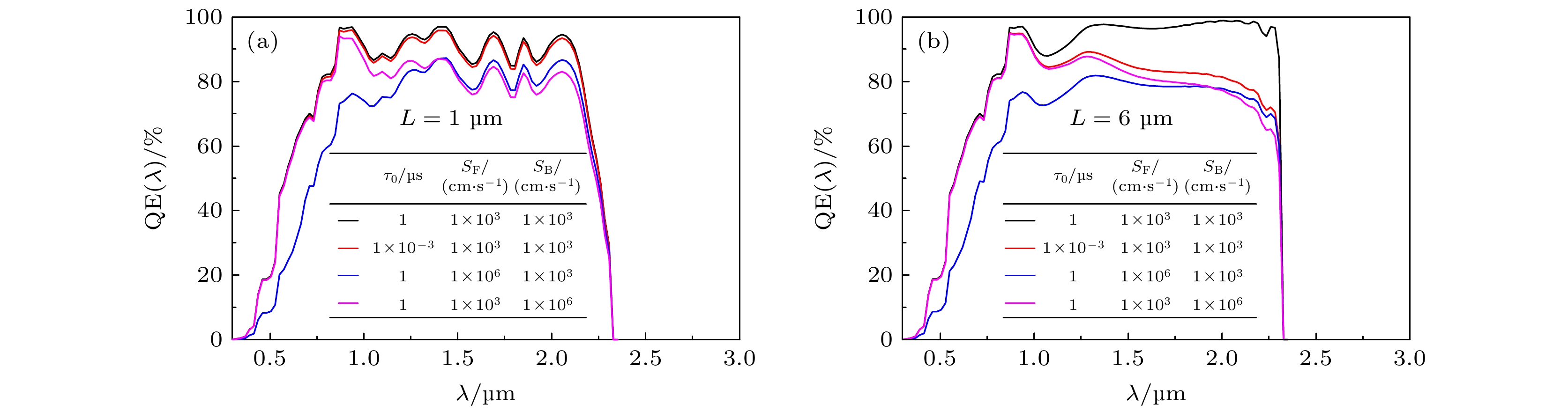
图 7 复合参数对不同厚度有源区量子效率谱QE(λ)的影响 (a) L = 1 µm; (b) L = 6 µm
Figure 7. Effects of the carrier recombination parameters on the quantum efficiency spectrums for different active region thickness L: (a) L = 1 µm; (b) L = 6 µm.
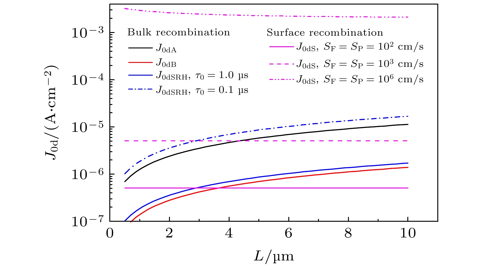
图 8 各种复合机制所决定的扩散暗电流密度随有源区厚度L的变化
Figure 8. Dependence of the diffusion dark current densities on active region thickness L.

图 9 室温下Ga0.84In0.16As0.14Sb0.86 p-n结的J0d随复合参数和L的变化
Figure 9. Dependence of the J0d on carrier recombination parameters and L for Ga0.84In0.16As0.14Sb0.86 p-n junction at room temperature.
表 1 室温(300 K)下Ga0.84In0.16As0.14Sb0.86 p-n结有源区的结构和物理参数[27-29]
Table 1. Structure and physical parameters of the Ga0.84In0.16As0.14Sb0.86 p-n junction at room temperature (300 K)[27-29].
材料 结构参数 物理参数 厚度/µm 掺杂浓
度/cm–3直接复合系
数/(cm3·s–1)俄歇复合系
数/(cm6·s–1)SRH本征复
合寿命/µs表面复合
速度/(cm·s–1)少子迁移
率/(cm2·V·s–1)n型层 0.2 1 × 10¹⁷ 1 × 10⁻¹⁰ Cn = 1 × 10–27 τ0 = 10–3—1 SF = 0—106 µh = 618 p型层 L—0.2 1 × 10¹⁷ Cp = 2 × 10–28 SB = 0—106 µe = 5162  DownLoad: CSV
-
[1] 刘超 魏志鹏 安宁 何斌太 刘鹏程 刘国军 2014 物理学报 63 248102
Google Scholar
Liu C, Wei Z P, An N, He B T, Liu P C, Liu G J 2014 Acta Phys. Sin. 63 248102
Google Scholar
[2] Mitsuhara M, Ohiso Y, Matsuzaki H 2020 J. Cryst. Growth 535 125551
Google Scholar
[3] Hao H Y, Wang G W, Han X, Jiang D W, Sun, Y Y, Guo C Y, Xiang W, Xu Y Q and Niu Z C 2018 AIP Adv. 8 095106
Google Scholar
[4] Lou Y Y, Zhang X L, Huang A B, Wang Y 2018 Sol. Energ. Mat. Sol. C. 172 124
[5] Liu Q, Marshall A, Kirer A 2019 Materials (Basel) 12 1743
Google Scholar
[6] Wang Y, Lou Y Y 2015 Renew. Energ. 75 8
Google Scholar
[7] You M H, Sun Q X, Yin L P, Fan J J, Liang X M, Li X, Yu X L, Li S J, Liu J S 2016 J. Nanomater. 2016 393502
[8] Liang B L, Chen D Y, Wang B, Kwasniewski T A, Wang Z G 2010 IEEE T. Electron Dev. 57 361
Google Scholar
[9] Rothmayr F, Pfenning A, Kistner C, Koeth J, Knebl G, Schade A, Krueger S, Worschech L, Hartmann F, Höfling S 2018 Appl. Phys. Lett. 112 161107
Google Scholar
[10] Peng X C, Guo X, Zhang B L, Li X P, Zhao X W, Dong X, Zheng W, Du G T 2010 Infrared Phys. Techn. 53 37
Google Scholar
[11] 秦飞飞 张海明 王彩霞 郭聪 张晶晶 2014 物理学报 63 198802
Google Scholar
Qin F F, Zhang H M, Wang C X, Guo C, Zhang J J 2014 Acta Phys. Sin. 63 198802
Google Scholar
[12] El-Batawy Y M, Deen M J 2003 Proc. SPIE 4999 363
Google Scholar
[13] Jiang A Q, Osamu Y, Chen L Y 2020 SCI REP-UK 10 12780
Google Scholar
[14] Chen H L, Cattoni A, Lépinau R D, Walker A W, Höhn O, Lackner D, Siefer G, Faustini M, Vandamme N, Goffard J, Behaghel B, Dupuis C, Bardou N, Dimroth F, Collin S 2019 Nat. energy 4 761
Google Scholar
[15] Amalathas A P, Alkaisi M M 2019 Micromachines 10 619
Google Scholar
[16] Proise F, Joudrier A, Pardo F, Pelouard J, Guillemoles J 2018 Opt. Express 26 A806
Google Scholar
[17] Yang Z H, Gao P Q, Zhang C, Li X F, Ye J C 2016 SCI REP-UK 6 30503
Google Scholar
[18] Kuznetsov A I, Miroshnichenko A E, Brongersma M L, Kivshar Y S, Luk’yanchuk B 2016 Science 354 aag2472
Google Scholar
[19] Jahani S, Jacob Z 2016 Nat. Nanotechnol. 11 23
Google Scholar
[20] Behaghel B, Tamaki R, Vandamme N, Watanabe K, Dupuis C, Bardou N, Sodabanlu H, Cattoni A, Okada Y, Sugiyama M, Collin S, Guillemoles J 2015 Appl. Phys. Lett. 106 081107
Google Scholar
[21] Peng X C, Wang Z D, Liu Y, Manos D M, Poelker M, Stutzman M, Tang B, Zhang S K, Zou J J 2019 Phys. Rev. Appl. 12 064002
Google Scholar
[22] 彭新村, 王智栋, 曾梦丝, 刘云, 邹继军, 朱志甫, 邓文娟 2019 无机材料学报 34 734
Google Scholar
Peng X C, Wang Z D, Zeng M S, Liu Y, Zou J J, Zhu Z F, Deng W J 2019 J. Inorg. Mater. 34 734
Google Scholar
[23] Wang C A, Shiau D A, Murphy P G, O'Brien P W, Huang R K, Connors M K, Anderson A C, Donetsky D, Anikeev S, Belenky G, Depoy D M, Nichols G 2004 J. Electron. Mater. 33 213
Google Scholar
[24] 彭新村 王智栋 邓文娟 朱志甫 邹继军 张益军 2020 物理学报 69 068501
Google Scholar
Peng X C, Wang Z D, Deng W J, Zhu Z F, Zou J J, Zhang Y J 2020 Acta Phys. Sin. 69 068501
Google Scholar
[25] Tian Y, Chua S J, Jin Y X 2003 Microelectron. J. 34 304
[26] Peng X C, Poelker M, Stutzman M, Tang B, Zhang S K, Zou J J 2020 Opt. Express 28 860
Google Scholar
[27] Wang Y, Chen N F, Zhang X W, Huang T M, Yin Z G, Wang Y S, Zhang H 2010 Sol. Energ. Mat. Sol. C. 94 1704
Google Scholar
[28] Tang L L, Fraas L M, Liu Z M, Xu C, Chen X Y 2016 IEEE T. Electron Dev. 63 3591
Google Scholar
[29] Dashiell M W, Beausang J F, Ehsani H, Nichols G J, Depoy D M, Danielson L R, Talamo P, Rahner K D, Brown E J, Burger S R, Fourspring P M, Topper W F, Jr., Baldasaro P F, Wang C A, Huang R K, Connors M K, Turner G W, Shellenbarger Z A, Taylor G, Li J Z, Martinelli R, Donetski D, Anikeev S, Belenky G L, Luryi S 2006 IEEE T. Electron Dev. 53 2879
Google Scholar
[30] Groep J, Polman A 2013 Opt. Express 21 26285
Google Scholar
[31] Wang Z Y, Zhang R J, Wang S Y, Lu M, Chen X, Zheng Y X, Chen L Y, Ye Z, Wang C Z, Ho K M 2015 SCI REP-UK 5 7810
Google Scholar
[32] Wang C A 2004 AIP Conf. Proc. 738 255
Google Scholar

 DownLoad:
Catalog
Metrics
- Abstract views: 6963
- PDF Downloads: 76
- Cited By: 0
