-
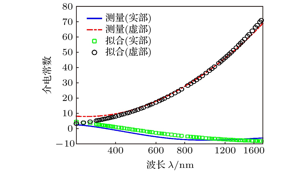
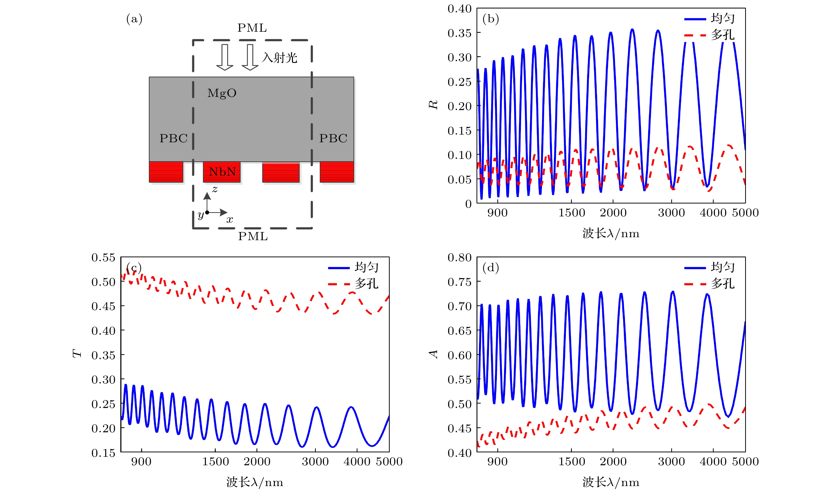
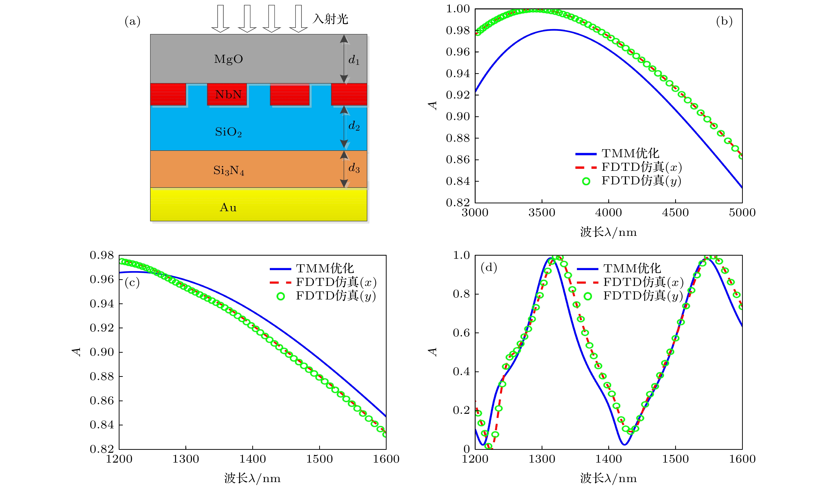
Nanoporous superconducting films with superconductor-insulator transition characteristics have potential application in the field of infrared photoelectric detection, but their broadband optical response characteristics in infrared band have not been reported. Therefore, taking nanoporous niobium nitride (NbN) films as the main object, the optical response characteristics in the near and medium infrared wavelength range of 780–5000 nm are studied in this paper. Firstly, the Drude-model fitting accuracy of measured NbN permittivity is improved by about 17%, and the NbN optical parameters in mid-infrared band are obtained. Furthermore, the optical response characteristics of the back-illuminated device with nanoporous NbN film are analyzed by finite difference time domain method, and a Bruggeman equivalent model which can simplify the nanoporous film into a uniform film is given, thereby reducing the three-dimensional simulation of nanoporous NbN film into one dimensional simulation. Finally, based on the equivalent model and the transfer matrix method, the light absorption characteristics of the back-illuminated device in near-/mid-infrared wavelength ranges are optimized. The results indicate that, on the one hand, simplifying the design process by using Bruggeman equivalent model will not affect the correctness of the final optimization results, and, on the other hand, a relatively simple optical cavity can make the detector achieve polarization-independent film absorption greater than 82% for near-/mid-infrared broadband design and 93.7% for double-wavelength design.
-
Keywords:
- nanoporous NbN film /
- infrared broadband photoresponse /
- Bruggeman theory /
- device structure design
[1] 胡伟达, 李庆, 陈效双, 陆卫 2019 物理学报 68 120701
 Google Scholar
Hu W D, Li Q, Chen X S, Lu W 2019 Acta Phys. Sin. 68 120701
 Google Scholar
[2] Lovell D 1969 Am. J. Phys. 37 467
 Google Scholar
[3] Lawson W, Nielsen S, Putley E, Young A 1959 J. Phys. Chem. Solids 9 325
 Google Scholar
[4] Esaki L, Tsu R 1970 IBM J. Res. Dev. 14 61
 Google Scholar
[5] Gol'tsman G N, Okunev O, Chulkova G, Lipatov A, Semenov A, Smirnov K, Voronov B, Dzardanov A, Williams C, Sobolewski R 2001 Appl. Phys. Lett. 79 705
 Google Scholar
[6] Novoselov K S, Geim A K, Morozov S V, Jiang D, Zhang Y, Dubonos S V, Grigorieva I V, Firsov A A 2004 Science 306 666
 Google Scholar
[7] Yang L, Jacob Z 2019 Opt. Express 27 10482
 Google Scholar
[8] Yang L, Jacob Z 2019 J. Appl. Phys. 126 174502
 Google Scholar
[9] Yang L, Jacob Z 2020 NPJ Quantum Inf. 6 76
 Google Scholar
[10] Sondhi S L, Girvin S M, Carini J P, Shahar D 1997 Rev. Mod. Phys. 69 315
 Google Scholar
[11] 李岚 2018 硕士学位论文 (成都: 电子科技大学)
Li L 2018 M. S. Thesis (Chengdu: University of Electronic Science and Technology of China) (in Chinese)
[12] Kapitulnik A, Kivelson B, Spivak B 2019 Rev. Mod. Phys. 91 011002
 Google Scholar
[13] Yang C, Liu Y, Wang Y, Feng L, He Q M, Sun J, Tang Y, Wu C C, Xiong J, Zhang W L, Lin X, Yao H, Liu H W, Fernandes G, Xu J, Valles J M, Wang Jian, Li Y R 2019 Science 366 1505
 Google Scholar
[14] Chen Z Y, Wang B Y, Swartz A G, Yoon H. Hikita Y, Raghu S, Hwang H Y 2021 npj Quantum Mater. 6 1
 Google Scholar
[15] Chen Z, Liu Y, Zhang H, Liu Z R, Tian H, Sun Y Q, Zhang M, Zhou Y, Sun J R, Xie Y W 2021 Science 372 721
 Google Scholar
[16] 吴洋, 陈奇, 徐睿莹, 葛睿, 张彪, 陶旭, 涂学凑, 贾小氢, 张蜡宝, 康琳, 吴培亨 2018 物理学报 67 248501
 Google Scholar
Wu Y, Chen Q, Xu R Y, Ge R, Zhang B, Tao X, Tu X C, Jia X Q, Zhang L B, Kang L, Wu P H 2018 Acta Phys. Sin. 67 248501
 Google Scholar
[17] Echtermeyer T, Milana S, Sassi U, Eiden A, Wu M, Lidorikis E, Ferrari A C 2016 Nano Lett. 16 8
 Google Scholar
[18] Hu X L, Cheng Y H, Gu C, Zhu X T, Liu H Y 2015 Sci. Bull. 60 1980
 Google Scholar
[19] Sunter K A, Berggren K K 2018 Appl. Opt. 57 4872
 Google Scholar
[20] Zheng F, Xu R Y, Chen Y J, Zhu G H, Jin B B, Kang L, Xu W W, Chen J, Wu P H 2017 IEEE Photonics J. 9 4502108
 Google Scholar
[21] 吴洋 2019 硕士学位论文 (南京: 南京大学)
Wu Y 2018 M. S. Thesis (Nanjing: Nanjing University) (in Chinese)
[22] Hu X L 2011 Ph. D. Dissertation (Cambridge: Massachusetts Institute of Technology)
[23] Hu X L, Marsili F, Najafi F, Berggren K K 2010 Proceedings of Quantum Electronics and Laser Science Conference San Jose, USA, May 16–21, 2010 pQThD5
[24] Khardani M, Bouaїcha M, Bessaїs B 2007 Phys. Status Solidi C 4 1986
 Google Scholar
[25] Stephens R E, Malitson I H 1952 J. Res. Nat. Bur. Stand. 49 249
 Google Scholar
-
-
[1] 胡伟达, 李庆, 陈效双, 陆卫 2019 物理学报 68 120701
 Google Scholar
Hu W D, Li Q, Chen X S, Lu W 2019 Acta Phys. Sin. 68 120701
 Google Scholar
[2] Lovell D 1969 Am. J. Phys. 37 467
 Google Scholar
[3] Lawson W, Nielsen S, Putley E, Young A 1959 J. Phys. Chem. Solids 9 325
 Google Scholar
[4] Esaki L, Tsu R 1970 IBM J. Res. Dev. 14 61
 Google Scholar
[5] Gol'tsman G N, Okunev O, Chulkova G, Lipatov A, Semenov A, Smirnov K, Voronov B, Dzardanov A, Williams C, Sobolewski R 2001 Appl. Phys. Lett. 79 705
 Google Scholar
[6] Novoselov K S, Geim A K, Morozov S V, Jiang D, Zhang Y, Dubonos S V, Grigorieva I V, Firsov A A 2004 Science 306 666
 Google Scholar
[7] Yang L, Jacob Z 2019 Opt. Express 27 10482
 Google Scholar
[8] Yang L, Jacob Z 2019 J. Appl. Phys. 126 174502
 Google Scholar
[9] Yang L, Jacob Z 2020 NPJ Quantum Inf. 6 76
 Google Scholar
[10] Sondhi S L, Girvin S M, Carini J P, Shahar D 1997 Rev. Mod. Phys. 69 315
 Google Scholar
[11] 李岚 2018 硕士学位论文 (成都: 电子科技大学)
Li L 2018 M. S. Thesis (Chengdu: University of Electronic Science and Technology of China) (in Chinese)
[12] Kapitulnik A, Kivelson B, Spivak B 2019 Rev. Mod. Phys. 91 011002
 Google Scholar
[13] Yang C, Liu Y, Wang Y, Feng L, He Q M, Sun J, Tang Y, Wu C C, Xiong J, Zhang W L, Lin X, Yao H, Liu H W, Fernandes G, Xu J, Valles J M, Wang Jian, Li Y R 2019 Science 366 1505
 Google Scholar
[14] Chen Z Y, Wang B Y, Swartz A G, Yoon H. Hikita Y, Raghu S, Hwang H Y 2021 npj Quantum Mater. 6 1
 Google Scholar
[15] Chen Z, Liu Y, Zhang H, Liu Z R, Tian H, Sun Y Q, Zhang M, Zhou Y, Sun J R, Xie Y W 2021 Science 372 721
 Google Scholar
[16] 吴洋, 陈奇, 徐睿莹, 葛睿, 张彪, 陶旭, 涂学凑, 贾小氢, 张蜡宝, 康琳, 吴培亨 2018 物理学报 67 248501
 Google Scholar
Wu Y, Chen Q, Xu R Y, Ge R, Zhang B, Tao X, Tu X C, Jia X Q, Zhang L B, Kang L, Wu P H 2018 Acta Phys. Sin. 67 248501
 Google Scholar
[17] Echtermeyer T, Milana S, Sassi U, Eiden A, Wu M, Lidorikis E, Ferrari A C 2016 Nano Lett. 16 8
 Google Scholar
[18] Hu X L, Cheng Y H, Gu C, Zhu X T, Liu H Y 2015 Sci. Bull. 60 1980
 Google Scholar
[19] Sunter K A, Berggren K K 2018 Appl. Opt. 57 4872
 Google Scholar
[20] Zheng F, Xu R Y, Chen Y J, Zhu G H, Jin B B, Kang L, Xu W W, Chen J, Wu P H 2017 IEEE Photonics J. 9 4502108
 Google Scholar
[21] 吴洋 2019 硕士学位论文 (南京: 南京大学)
Wu Y 2018 M. S. Thesis (Nanjing: Nanjing University) (in Chinese)
[22] Hu X L 2011 Ph. D. Dissertation (Cambridge: Massachusetts Institute of Technology)
[23] Hu X L, Marsili F, Najafi F, Berggren K K 2010 Proceedings of Quantum Electronics and Laser Science Conference San Jose, USA, May 16–21, 2010 pQThD5
[24] Khardani M, Bouaїcha M, Bessaїs B 2007 Phys. Status Solidi C 4 1986
 Google Scholar
[25] Stephens R E, Malitson I H 1952 J. Res. Nat. Bur. Stand. 49 249
 Google Scholar
Catalog
Metrics
- Abstract views: 6694
- PDF Downloads: 91
- Cited By: 0


 DownLoad:


