


-
Bismuth (Bi), as a stable heaviest element in the periodic table of elements, has strong spin-orbit coupling, which has attracted a lot of attention as the parent material of various known topological insulators. Previous calculations predicted that Bi(111) with a thickness less than eight bilayers and the ultrathin black-phosphorus-like Bi(110) films are single-element two-dimensional (2D) topological insulators. However, it is generally believed that these crystalline bismuth phases are not superconducting or their transition temperature should be lower than 0.5 mK. Lead (Pb) is a good superconducting elementary material, and there is a relatively small difference in radius between the Bi atom and Pb atom. According to the Hume-Rothery rule, it is expected that Pb/Bi alloys in an arbitrary ratio should be superconducting. One may thus expect to form crystalline Bi based superconductors by Pb substitution, which might host intriguing topological superconductivity. While our previous work has demonstrated a low-temperature stable Pb1–xBix (x~0.1) alloy phase in which Pb in the Pb(111) structure is partially replaced by Bi, the Bi crystalline structure-based phases of the superconducting alloys still lack in-depth research. Here, we report a new low-temperature phase of Pb-Bi alloy thin film, namely PbBi3, on the Si(111)-(7 × 7) substrate, by co-depositing Pb and Bi at a low temperature of about 100 K followed by an annealing treatment of 200 K for 2 h. Using low-temperature scanning tunneling microscopy and spectroscopy (STM/STS), we characterize in situ the surface structure and superconducting properties of the Pb-Bi alloy film with a nominal thickness of about 4.8 nm. Two spatially separated phases with quasi-tetragonal structure are observed in the surface of the Pb-Bi alloy film, which can be identified as the pure Bi(110) phase and the PbBi3 phase, respectively, based on their distinct atomic structures, step heights and STS spectra. The PbBi3 film has a base structure similar to Bi(110), where about 25% of the Bi atoms are replaced by Pb, and the surface shows a
$\sqrt 2 \times \sqrt 2 R{45^ \circ }$ reconstructed structure. The superconducting behavior of the PbBi3 phase is characterized using variable-temperature STS spectra. We obtain that the superconducting transition temperature of PbBi3 is about 6.13 K, and the$2\varDelta (0)/{k_{\text{B}}}{T_{\text{c}}}$ ratio is about 4.62 using the fitting parameter of$\varDelta (0) = 1.22{\text{ meV}}$ at 0 K. By measuring the magnetic field dependent superconducting coherence length, the critical field is estimated at larger than 0.92 T. We further investigate the superconducting proximity effect in the normal metal-superconductor (N-S) heterojunction consisting of the non-superconducting Bi(110) domain and the superconducting PbBi3 domain. The N-S heterojunctions with both in-plane configuration and step-like configuration are measured, which suggest that the atomic connection and the area of the quasi-2D Josephson junctions and the external magnetic field can affect the lateral superconducting penetration length. We also observe the zero-bias conductance peaks (ZBCPs) in the superconducting gap of the PbBi3 surface in some cases at zero magnetic field. By measuring dI/dV spectra at various temperatures and by adopting a superconducting Nb tip, we identify that the ZBCP originates from the superconductor-insulator-superconductor (S-I-S) junction formed between a superconducting tip and the sample. Nevertheless, the Bi(110)-based PbBi3 phase may provide a possible platform to explore the intriguing topological superconducting behaviors at the vortexes under magnetic fields, or in the vicinity of the potentially topological superconducting Bi(110) islands by considering the proximity effect.-
Keywords:
- bismuth-lead alloy /
- superconducting coherence length /
- proximity effect /
- zero-bias conductance peak
[1] Wang Z, Sun Y, Chen X Q, Franchini C, Xu G, Weng H, Dai X, Fang Z 2012 Phys. Rev. B 85 195320
 Google Scholar
[2] Bansil A, Lin H, Das T 2016 Rev. Mod. Phys. 88 021004
Google Scholar
[3] Autès G, Isaeva A, Moreschini L, Johannsen J C, Pisoni A, Mori R, Zhang W, Filatova T G, Kuznetsov A N, Forró L, Van den Broek W, Kim Y, Kim K S, Lanzara A, Denlinger J D, Rotenberg E, Bostwick A, Grioni M, Yazyev O V 2016 Nat. Mater. 15 154
Google Scholar
[4] Liu C C, Zhou J J, Yao Y, Zhang F 2016 Phys. Rev. Lett. 116 066801
Google Scholar
[5] Murakami S 2006 Phys. Rev. Lett. 97 236805
Google Scholar
[6] Wada M, Murakami S, Freimuth F, Bihlmayer G 2011 Phys. Rev. B 83 121310
Google Scholar
[7] Lu Y, Xu W, Zeng M, Yao G, Shen L, Yang M, Luo Z, Pan F, Wu K, Das T, He P, Jiang J, Martin J, Feng Y P, Lin H, Wang X S 2015 Nano Lett. 15 80
Google Scholar
[8] Hofmann P 2006 Prog. Surf. Sci. 81 191
Google Scholar
[9] Prakash O, Kumar A, Thamizhavel A, Ramakrishnan S 2017 Science 355 52
Google Scholar
[10] Dolan G J, Silcox J 1973 Phys. Rev. Lett. 30 603
Google Scholar
[11] Zhang T, Cheng P, Li W J, Sun Y J, Wang G, Zhu X G, He K, Wang L L, Ma X C, Chen X, Wang Y Y, Liu Y, Lin H Q, Jia J F, Xue Q K 2010 Nat. Phys. 6 104
Google Scholar
[12] Uchihashi T 2017 Supercond. Sci. Technol. 30 013002
Google Scholar
[13] Egami T, Waseda Y 1984 J. Non-Cryst. Solids 64 113
Google Scholar
[14] Adler J G, Ng S C 1965 Can. J. Phys. 43 594
Google Scholar
[15] Chen T T, Leslie J D, Smith H J T 1971 Physica 55 439
Google Scholar
[16] Dynes R C, Rowell J M 1975 Phys. Rev. B 11 1884
Google Scholar
[17] Gokcen N A 1992 J. Phase Equil. 13 21
Google Scholar
[18] Fujime S 1966 Japan. J. Appl. Phys. 5 59
Google Scholar
[19] Borromee-Gautier C, Giessen B C, Grant N J 1968 J. Chem. Phys. 48 1905
Google Scholar
[20] 田明阳, 王巨丰, 杜宏健, 马传许, 王兵 2021 物理学报 70 170703
Google Scholar
Tian M Y, Wang J F, Du H J, Ma C X, Wang B 2021 Acta Phys. Sin. 70 170703
Google Scholar
[21] Dynes R C, Narayanamurti V, Garno J P 1978 Phys. Rev. Lett. 41 1509
Google Scholar
[22] Liu J, Wu X, Ming F, Zhang X, Wang K, Wang B, Xiao X 2011 J. Phys. Condens. Matter 23 265007
Google Scholar
[23] Ning Y, Song C, Wang Y, Chen X, Jia J, Xue Q, Ma X 2010 J. Phys. Condens. Matter 22 065701
Google Scholar
[24] Eskildsen M, Kugler M, Tanaka S, Jun J, Kazakov S, Karpinski J, Fischer Ø 2002 Phys. Rev. Lett. 89 187003
Google Scholar
[25] Yaginuma S, Nagao T, Sadowski J, Saito M, Nagaoka K, Fujikawa Y, Sakurai T, Nakayama T 2007 Surf. Sci. 601 3593
Google Scholar
[26] Yuhara J, Yokoyama M, Matsui T 2011 J. Appl. Phys. 110 074314
Google Scholar
[27] 刘建宇, 孙昊桦, 管丹丹, 李耀义, 王世勇, 刘灿华, 郑浩, 贾金锋 2018 物理学报 67 170701
Google Scholar
Liu J Y, Sun H H, Guan D D, Li Y Y, Wang S Y, Liu C H, Zheng H, Jia J F 2018 Acta Phys. Sin. 67 170701
Google Scholar
[28] Yaginuma S, Nagaoka K, Nagao T, Bihlmayer G, Koroteev Y M, Chulkov E V, Nakayama T 2008 J. Phys. Soc. Jpn. 77 014701
Google Scholar
[29] Nagase K, Kokubo I, Yamazaki S, Nakatsuji K, Hirayama H 2018 Phys. Rev. B 97 195418
Google Scholar
[30] Ning Y, Song C, Guan Z, Ma X, Chen X, Jia J, Xue Q 2009 EPL 85 27004
Google Scholar
[31] Sonier J E 2004 J. Phys. Condens. Matter 16 S4499
Google Scholar
[32] Brun C, Cren T, Cherkez V, Debontridder F, Pons S, Fokin D, Tringides M C, Bozhko S, Ioffe L B, Altshuler B L, Roditchev D 2014 Nat. Phys. 10 444
Google Scholar
[33] Yoshizawa S, Kim H, Kawakami T, Nagai Y, Nakayama T, Hu X, Hasegawa Y, Uchihashi T 2014 Phys. Rev. Lett. 113 247004
Google Scholar
[34] Andreev A F 1964 Sov. Phys. JETP 19 1228
[35] Kim J, Chua V, Fiete G A, Nam H, MacDonald A H, Shih C K 2012 Nat. Phys. 8 464
Google Scholar
[36] Usadel K D 1970 Phys. Rev. Lett. 25 507
Google Scholar
[37] Sasaki S, Kriener M, Segawa K, Yada K, Tanaka Y, Sato M, Ando Y 2011 Phys. Rev. Lett. 107 217001
Google Scholar
[38] Yu W, Haenel R, Rodriguez M A, Lee S R, Zhang F, Franz M, Pikulin D I, Pan W 2020 Phys. Rev. Research 2 032002(R
Google Scholar
[39] Blackford B L, March R H 1968 Can. J. Phys. 46 141
Google Scholar
[40] 张裕恒 2009 超导物理 (第三版) (合肥: 中国科学技术大学出版社) 第348—351页
Zhang Y H 2009 Superconducting Physics (3rd Ed.) (Hefei: University of Science and Technology of China Press) pp348–351 (in Chinese)
[41] Suderow H, Crespo V, Guillamon I, Vieira S, Servant F, Lejay P, Brison J, Flouquet J 2009 New J. Phys. 11 093004
Google Scholar
[42] Ternes M, Schneider W D, Cuevas J C, Lutz C P, Hirjibehedin C F, Heinrich A J 2006 Phys. Rev. B 74 132501
Google Scholar
[43] Majorana E 1937 Il. Nuovo. Cimento. 14 171
Google Scholar
[44] Xu J P, Wang M X, Liu Z L, Ge J F, Yang X, Liu C, Xu Z A, Guan D, Gao C L, Qian D, Liu Y, Wang Q H, Zhang F C, Xue Q K, Jia J F 2015 Phys. Rev. Lett. 114 017001
Google Scholar
[45] Sun H H, Zhang K W, Hu L H, Li C, Wang G Y, Ma H Y, Xu Z A, Gao C L, Guan D D, Li Y Y, Liu C, Qian D, Zhou Y, Fu L, Li S C, Zhang F C, Jia J F 2016 Phys. Rev. Lett. 116 257003
Google Scholar
-

图 1 Pb-Bi合金薄膜的生长和结构表征 (a), (b) 0.4 K下获得的样品表面大范围STM形貌图像及对应区域的零偏压电导图像, 扫描条件: (a) 样品偏压Vs = –90 mV, 隧穿电流It = 20 pA, 扫描尺寸为500 nm × 500 nm; (b) Vs = –10 mV, It = 1 nA. (c), (d) α和β区域台阶高度分布的统计结果(统计不同区域的约100幅大范围STM图像); (e), (f) α区域的STM原子图像及其FFT图谱; (g), (h) β区域的STM原子图像及其FFT图谱; (e), (g)扫描条件为 Vs = –10 mV, It = 1 nA, 扫描尺寸为5 nm × 5 nm; (i) 沿(g)图中青色直线的高度轮廓线, 其中较高和较低的原子可分别归属为Pb和Bi原子; (j) PbBi3薄膜结构模型的俯视和侧视图
Figure 1. Surface structure of the Pb-Bi alloy film: (a) STM topography image of the alloy surface at 0.4 K (sample bias Vs = –90 mV and tunneling current It = 20 pA, 500 nm × 500 nm); (b) zero-bias conductance (ZBC) image acquired at 0.4 K within the same area in Fig. (a); (c) and (d) step height distributions of α and β phases counted in around 100 images; (e) and (f) atomically-resolved STM image (Vs = –10 mV and It = 1 nA, 5 nm × 5 nm) and corresponding FFT pattern of the α phase; (g) and (h) atomically-resolved STM image (Vs = –10 mV and It = 1 nA, 5 nm × 5 nm) and corresponding FFT pattern of the β phase; (i) height profile taken along the cyan line in Fig. (g), where the higher and lower atoms can be assigned as Pb and Bi atoms, respectively; (j) schematics of the top and side views of the PbBi3 alloy structure.
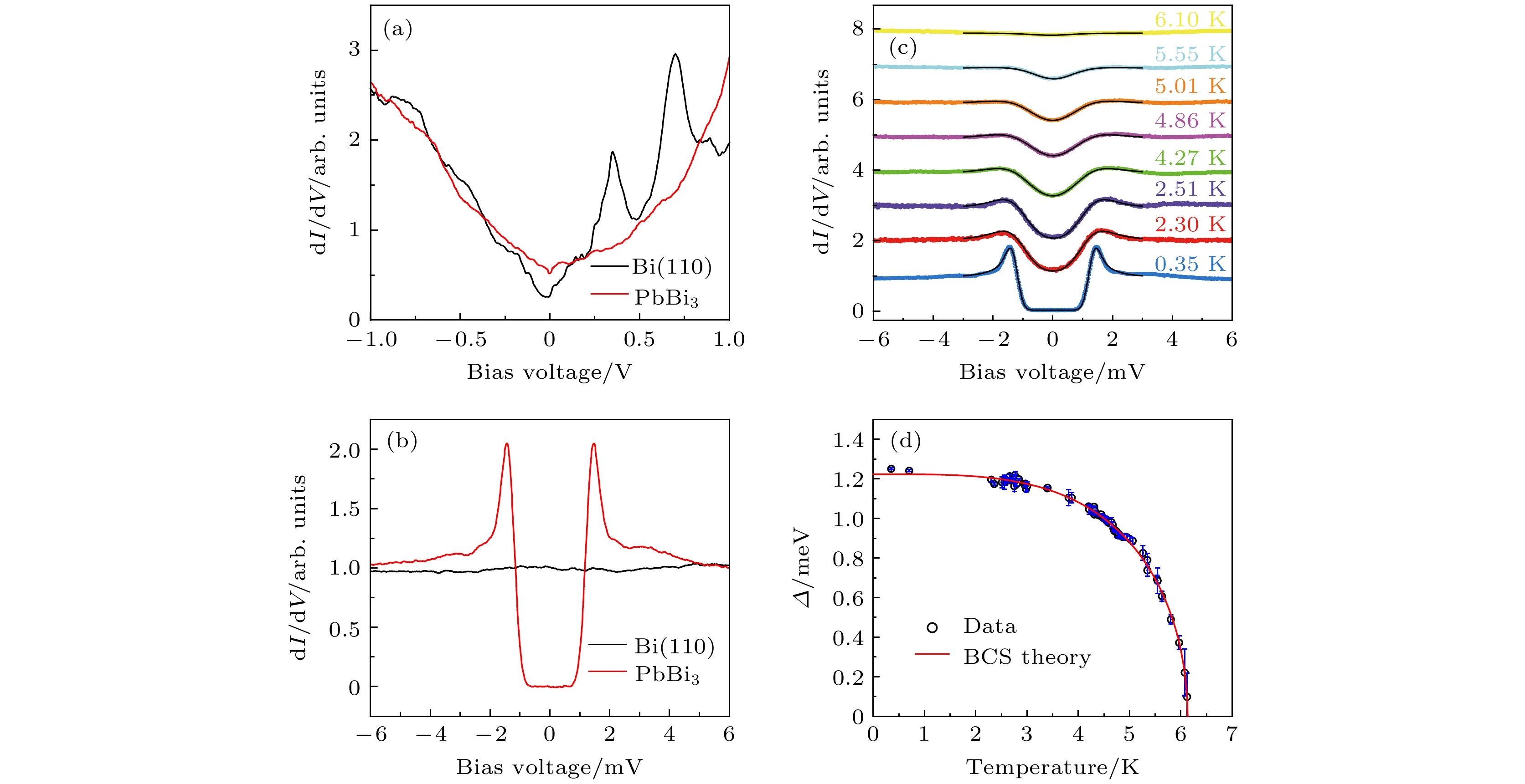
图 2 PbBi3合金薄膜的超导物性表征 (a), (b) 0.4 K下在Bi(110)(黑线)和PbBi3(红线)表面区域采集的不同能量范围的典型dI/dV谱, 采谱条件: (a) Vs = –1 V, It = 2 nA, 调制偏压Vmod = 2 mV; (b) Vs = –10 mV, It = 1 nA, Vmod = 100 μV. (c) PbBi3相变温dI/dV谱, 叠加在实验谱线上的黑线曲线 (±3 mV) 是基于BCS理论对能隙的拟合. 采谱条件: Vs = –10 mV, It = 1 nA, Vmod = 100 μV. (d) 超导能隙大小和温度的依赖关系及BCS拟合
Figure 2. Superconducting properties of PbBi3 alloy thin films: (a), (b) Representative dI/dV spectra acquired from the Bi(110) region (black line) and the PbBi3 region (red line), measured with a W tip at 0.4 K in different energy ranges ((a) Vs = –1 V, It = 2 nA, Vmod = 2 mV; (b) Vs = –10 mV, It = 1 nA, Vmod = 100 μV). (c) Temperature-dependent dI/dV spectra of the PbBi3 phase, overlaid with the fitting curves (in black, ±3 mV) on the basis of BCS theory. The spectra are shifted vertically for clarity (Vs = –10 mV, It = 1 nA, Vmod = 100 μV). (d) Temperature dependence of the superconducting energy gap extracted from Fig. (c) (black circles) and fitting with temperature-dependent superconducting gap
$ \varDelta(T) $ (red line) using BCS theory.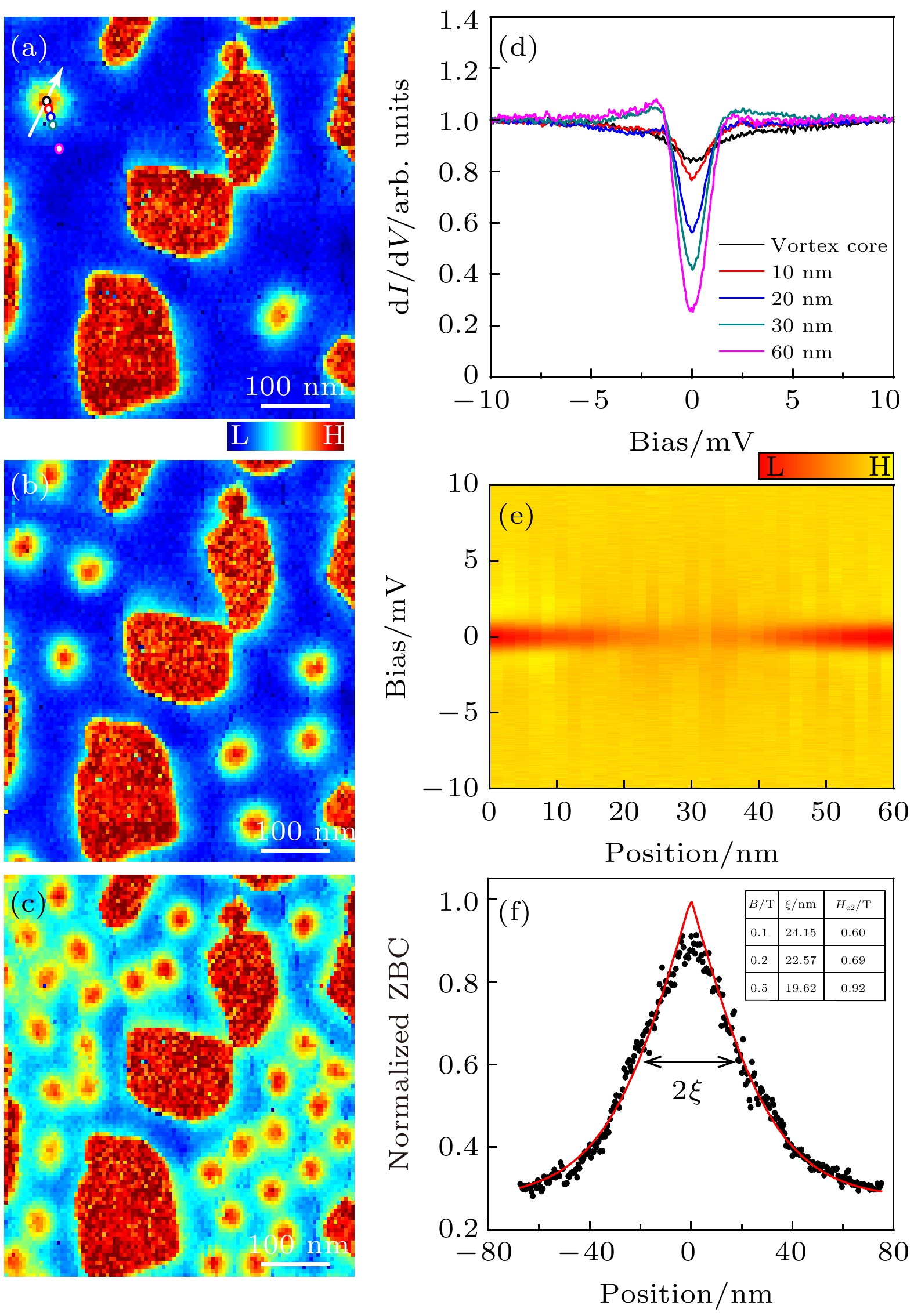
图 3 PbBi3合金薄膜的磁通涡旋态 (a)—(c) 0.4 K下样品同一区域在0.1, 0.2和0.5 T外加垂直磁场下的零偏压电导成像, 采谱条件: Vs = –10 mV, It = 1 nA, Vmod = 100 μV, 图像尺寸为500 nm × 500 nm. (d) 0.1 T磁场下距离磁通涡旋中心不同位置的dI/dV谱, 作谱位置如图(a)中彩色圆圈所示; 采谱条件: Vs = –10 mV, It = 1 nA, Vmod = 100 μV. (e) 沿着图(a)中白色线采集的30条dI/dV得到的电导分布图; (f) 归一化零偏压电导在磁通涡旋上的分布及拟合结果
Figure 3. Magnetic flux vortex state of PbBi3 alloy thin films : (a)–(c) normalized ZBC image measured at 0.4 K under different magnetic fields (0.1, 0.2 and 0.5 T)(Vs = –10 mV, It = 1 nA, Vmod = 100 μV, 500 nm × 500 nm). (d) A series of differential conductance spectra obtained at vortex core and 10, 20, 30 and 60 nm off vortex core under 0.1 T magnetic field, as marked by colored dots in Fig. (a) (Vs = –10 mV, It = 1 nA, Vmod = 100 μV). (e) Two-dimensional (2D) conductance map plotted with 30 dI/dV curves taken along the white line through the vortex in Fig. (a). (f) ZBC profile (black dots) across the vortex core under 0.1 T. The red curve is a theoretical fitting which gives a value of the superconducting coherence length
$\xi = (24.15 \pm 0.20)$ nm.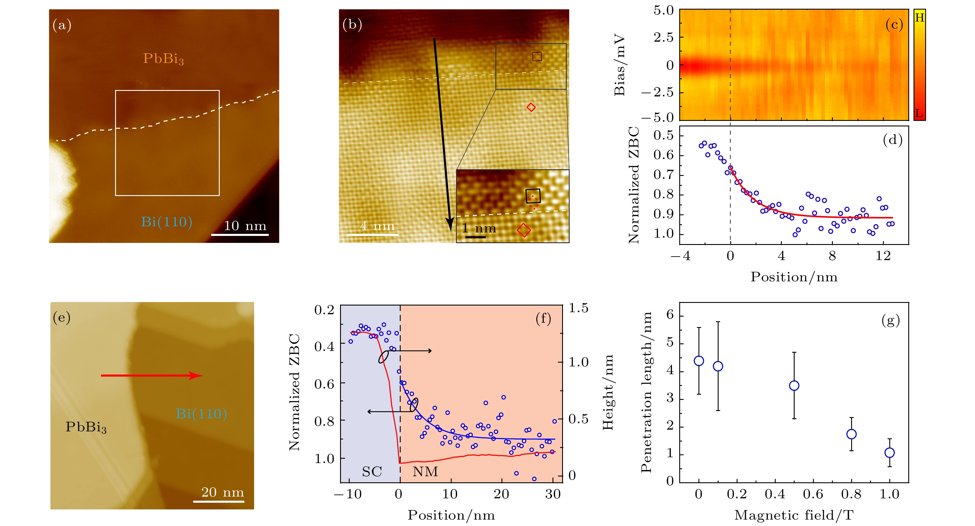
图 4 正常金属-超导体(N-S)异质结处的邻近效应 (a) 共面型N-S异质结的大范围STM形貌像; (b) 图(a)中白色正方形区域的异质结原子分辨图像; 扫描条件: (a) Vs = –50 mV, It = 1 nA, 图像尺寸为40 nm × 40 nm; (b) Vs = –10 mV, It = 1 nA, 图像尺寸为20 nm × 20 nm. (c) 沿(b)中黑色带箭头直线所采的60条dI/dV谱绘成的二维电导图像, 采谱条件: Vs = –10 mV, It = 1 nA, Vmod = 100 μV. (d) 从图(c)中提取的N-S结归一化的零偏压电导的空间分布, 蓝色圆圈是实验数据, 红色线是指数衰减拟合结果, 拟合公式为
$ - 0.25{{\text{e}}^{ - x/1.84}} + 0.91$ ; 这里x为距离界面的位置坐标. (e) 台阶型N-S异质结的STM形貌像, 扫描条件: Vs = –90 mV, It = 1 nA, 图像尺寸为80 nm × 80 nm. (f) 0.5 T磁场下沿图(e)中红色带箭头直线获得的N-S结归一化零偏压电导的空间分布, 蓝色曲线是指数衰减拟合结果, 拟合公式为$ - 0.32{{\text{e}}^{ - x/3.50}} + 0.90$ ; 红色实线是对应的异质结表面高度轮廓线. 图(c), (d)和(f)中, 黑色虚线为异质结界面位置. (g) 图(e)中台阶型N-S异质结的超导邻近效应穿透深度随磁场的依赖关系Figure 4. Proximity effect at normal metal-superconductor (N-S) heterojunctions: (a) Large-area STM image of the alloy surface, showing an in-plane N-S heterojunction (Vs = –50 mV, It = 1 nA, 40 nm × 40 nm). (b) High-resolution STM image of the white square region in Fig. (a) (Vs = –10 mV, It = 1 nA, 20 nm × 20 nm). (c) 2D conductance map plotted with 60 normalized dI/dV spectra acquired across the in-plane N-S heterojunction along the arrowed black line in Fig. (b) (Vs = –10 mV, It = 1 nA, Vmod = 100 μV). (d) Plot of the normalized ZBC extracted from Fig. (c). The red curve is exponential fitting of the data with function as
$ - 0.25{{\text{e}}^{ - x/1.84}} + 0.91$ , where x is the distance away from the lower step edge. (e) Large-area STM image showing another N-S heterojunction with different heights for the Bi(110) and PbBi3 sides (Vs = –90 mV, It = 1 nA, 80 nm × 80 nm). (f) Height profile (red curve) and the normalized ZBC (blue circles) along the arrowed red line in Fig. (e), acquired at a magnetic field strength B = 0.5 T. The blue curve is exponential fitting of the data with function as$ - 0.32{{\text{e}}^{ - x/3.50}} + 0.90$ . In Figs. (c), (d) and (f), the conductance at the setpoint bias (Vs = –10 mV) in the dI/dV curves is normalized to 1. The dashed lines indicate the interfaces of the N-S heterojunctions in Figs. (c), (d) and (f). (g) B-dependent lateral superconducting penetration length in the step-type N-S heterojunction shown in Fig. (e).
图 5 超导针尖引起的零偏压电导峰现象 (a) 在PbBi3表面(4.2 K(红色)和0.4 K(黑色))和Bi(110) 表面(4.2 K, 蓝色)采集的dI/dV谱; 采谱条件: Vs = –10 mV, It = 1 nA, Vmod = 100 μV. (b) 不同温度下PbBi3表面的dI/dV谱, 叠加在实验谱线上的黑色曲线(±5 mV)是基于BCS理论对能隙的拟合; 采谱条件: Vs = –10 mV, It = 1 nA, Vmod = 100 μV. (c) 超导能隙大小和温度的依赖关系及拟合结果; (d) 不同温度下, 用超导Nb针尖在PbBi3表面得到的dI/dV谱(Vs = –10 mV, It = 1 nA, Vmod = 100 μV); (e) 0.4 K 下Nb针尖获得的dI/dV谱随隧道结电阻的变化(Vs = –10 mV, Vmod = 100 μV, It = 1 nA (10 MΩ), 2 nA (5 MΩ), 10 nA (1 MΩ), 100 nA (100 kΩ), 200 nA (50 kΩ), 500 nA (20 kΩ), 1 μA (10 kΩ), 2 μA (5 kΩ))
Figure 5. Properties and origin of ZBCP: (a) dI/dV spectra taken on PbBi3 (black at 0.4 K; red at 4.2 K) and Bi(110) (blue at 4.2 K) region. (b) Temperature-dependent dI/dV spectra of the PbBi3 region, overlaid with the fitting curves (in black) on the basis of BCS theory, and the spectra are shifted vertically for clarity. (c) Temperature dependence of the superconducting energy gap
$\varDelta(T)$ extracted from Fig. (b) (black dots) and fitting with temperature-dependent superconducting gap (red line) using BCS theory, assuming a superconducting tip with gap${\varDelta _{{\text{tip}}}} = {\varDelta _{{\text{sample}}}}$ . The extracted superconducting gap of 1.27 meV and Tc = 6.25 K are similar to the result obtained in Fig. 2(d). (d) Two spectra taken on the PbBi3 surface at 4.2 and 0.4 K with a superconducting Nb tip (Vs = –10 mV, It = 1 nA, Vmod = 100 μV). (e) The evolution of spectra with the decrease of tunneling junction’s impedance at 0.4 K with a superconducting Nb tip (Vs = –10 mV, Vmod = 100 μV, It = 1 nA (10 MΩ), 2 nA (5 MΩ), 10 nA (1 MΩ), 100 nA (100 kΩ), 200 nA (50 kΩ), 500 nA (20 kΩ), 1 μA (10 kΩ), 2 μA (5 kΩ)). -
[1] Wang Z, Sun Y, Chen X Q, Franchini C, Xu G, Weng H, Dai X, Fang Z 2012 Phys. Rev. B 85 195320
Google Scholar
[2] Bansil A, Lin H, Das T 2016 Rev. Mod. Phys. 88 021004
Google Scholar
[3] Autès G, Isaeva A, Moreschini L, Johannsen J C, Pisoni A, Mori R, Zhang W, Filatova T G, Kuznetsov A N, Forró L, Van den Broek W, Kim Y, Kim K S, Lanzara A, Denlinger J D, Rotenberg E, Bostwick A, Grioni M, Yazyev O V 2016 Nat. Mater. 15 154
Google Scholar
[4] Liu C C, Zhou J J, Yao Y, Zhang F 2016 Phys. Rev. Lett. 116 066801
Google Scholar
[5] Murakami S 2006 Phys. Rev. Lett. 97 236805
Google Scholar
[6] Wada M, Murakami S, Freimuth F, Bihlmayer G 2011 Phys. Rev. B 83 121310
Google Scholar
[7] Lu Y, Xu W, Zeng M, Yao G, Shen L, Yang M, Luo Z, Pan F, Wu K, Das T, He P, Jiang J, Martin J, Feng Y P, Lin H, Wang X S 2015 Nano Lett. 15 80
Google Scholar
[8] Hofmann P 2006 Prog. Surf. Sci. 81 191
Google Scholar
[9] Prakash O, Kumar A, Thamizhavel A, Ramakrishnan S 2017 Science 355 52
Google Scholar
[10] Dolan G J, Silcox J 1973 Phys. Rev. Lett. 30 603
Google Scholar
[11] Zhang T, Cheng P, Li W J, Sun Y J, Wang G, Zhu X G, He K, Wang L L, Ma X C, Chen X, Wang Y Y, Liu Y, Lin H Q, Jia J F, Xue Q K 2010 Nat. Phys. 6 104
Google Scholar
[12] Uchihashi T 2017 Supercond. Sci. Technol. 30 013002
Google Scholar
[13] Egami T, Waseda Y 1984 J. Non-Cryst. Solids 64 113
Google Scholar
[14] Adler J G, Ng S C 1965 Can. J. Phys. 43 594
Google Scholar
[15] Chen T T, Leslie J D, Smith H J T 1971 Physica 55 439
Google Scholar
[16] Dynes R C, Rowell J M 1975 Phys. Rev. B 11 1884
Google Scholar
[17] Gokcen N A 1992 J. Phase Equil. 13 21
Google Scholar
[18] Fujime S 1966 Japan. J. Appl. Phys. 5 59
Google Scholar
[19] Borromee-Gautier C, Giessen B C, Grant N J 1968 J. Chem. Phys. 48 1905
Google Scholar
[20] 田明阳, 王巨丰, 杜宏健, 马传许, 王兵 2021 物理学报 70 170703
Google Scholar
Tian M Y, Wang J F, Du H J, Ma C X, Wang B 2021 Acta Phys. Sin. 70 170703
Google Scholar
[21] Dynes R C, Narayanamurti V, Garno J P 1978 Phys. Rev. Lett. 41 1509
Google Scholar
[22] Liu J, Wu X, Ming F, Zhang X, Wang K, Wang B, Xiao X 2011 J. Phys. Condens. Matter 23 265007
Google Scholar
[23] Ning Y, Song C, Wang Y, Chen X, Jia J, Xue Q, Ma X 2010 J. Phys. Condens. Matter 22 065701
Google Scholar
[24] Eskildsen M, Kugler M, Tanaka S, Jun J, Kazakov S, Karpinski J, Fischer Ø 2002 Phys. Rev. Lett. 89 187003
Google Scholar
[25] Yaginuma S, Nagao T, Sadowski J, Saito M, Nagaoka K, Fujikawa Y, Sakurai T, Nakayama T 2007 Surf. Sci. 601 3593
Google Scholar
[26] Yuhara J, Yokoyama M, Matsui T 2011 J. Appl. Phys. 110 074314
Google Scholar
[27] 刘建宇, 孙昊桦, 管丹丹, 李耀义, 王世勇, 刘灿华, 郑浩, 贾金锋 2018 物理学报 67 170701
Google Scholar
Liu J Y, Sun H H, Guan D D, Li Y Y, Wang S Y, Liu C H, Zheng H, Jia J F 2018 Acta Phys. Sin. 67 170701
Google Scholar
[28] Yaginuma S, Nagaoka K, Nagao T, Bihlmayer G, Koroteev Y M, Chulkov E V, Nakayama T 2008 J. Phys. Soc. Jpn. 77 014701
Google Scholar
[29] Nagase K, Kokubo I, Yamazaki S, Nakatsuji K, Hirayama H 2018 Phys. Rev. B 97 195418
Google Scholar
[30] Ning Y, Song C, Guan Z, Ma X, Chen X, Jia J, Xue Q 2009 EPL 85 27004
Google Scholar
[31] Sonier J E 2004 J. Phys. Condens. Matter 16 S4499
Google Scholar
[32] Brun C, Cren T, Cherkez V, Debontridder F, Pons S, Fokin D, Tringides M C, Bozhko S, Ioffe L B, Altshuler B L, Roditchev D 2014 Nat. Phys. 10 444
Google Scholar
[33] Yoshizawa S, Kim H, Kawakami T, Nagai Y, Nakayama T, Hu X, Hasegawa Y, Uchihashi T 2014 Phys. Rev. Lett. 113 247004
Google Scholar
[34] Andreev A F 1964 Sov. Phys. JETP 19 1228
[35] Kim J, Chua V, Fiete G A, Nam H, MacDonald A H, Shih C K 2012 Nat. Phys. 8 464
Google Scholar
[36] Usadel K D 1970 Phys. Rev. Lett. 25 507
Google Scholar
[37] Sasaki S, Kriener M, Segawa K, Yada K, Tanaka Y, Sato M, Ando Y 2011 Phys. Rev. Lett. 107 217001
Google Scholar
[38] Yu W, Haenel R, Rodriguez M A, Lee S R, Zhang F, Franz M, Pikulin D I, Pan W 2020 Phys. Rev. Research 2 032002(R
Google Scholar
[39] Blackford B L, March R H 1968 Can. J. Phys. 46 141
Google Scholar
[40] 张裕恒 2009 超导物理 (第三版) (合肥: 中国科学技术大学出版社) 第348—351页
Zhang Y H 2009 Superconducting Physics (3rd Ed.) (Hefei: University of Science and Technology of China Press) pp348–351 (in Chinese)
[41] Suderow H, Crespo V, Guillamon I, Vieira S, Servant F, Lejay P, Brison J, Flouquet J 2009 New J. Phys. 11 093004
Google Scholar
[42] Ternes M, Schneider W D, Cuevas J C, Lutz C P, Hirjibehedin C F, Heinrich A J 2006 Phys. Rev. B 74 132501
Google Scholar
[43] Majorana E 1937 Il. Nuovo. Cimento. 14 171
Google Scholar
[44] Xu J P, Wang M X, Liu Z L, Ge J F, Yang X, Liu C, Xu Z A, Guan D, Gao C L, Qian D, Liu Y, Wang Q H, Zhang F C, Xue Q K, Jia J F 2015 Phys. Rev. Lett. 114 017001
Google Scholar
[45] Sun H H, Zhang K W, Hu L H, Li C, Wang G Y, Ma H Y, Xu Z A, Gao C L, Guan D D, Li Y Y, Liu C, Qian D, Zhou Y, Fu L, Li S C, Zhang F C, Jia J F 2016 Phys. Rev. Lett. 116 257003
Google Scholar


 DownLoad:


Catalog
Metrics
- Abstract views: 10253
- PDF Downloads: 368
- Cited By: 0
