


SPECIAL TOPIC—Novel properties of low-dimensional materials


2022, 71 (12): 126101.
doi: 10.7498/aps.71.20220035
Abstract +
Exploring the structure of low-dimensional materials is a key step towards a complete understanding of condensed matter. In recent years, owing to the fast developing of research tools, novel structures of many elements have been reported, revealing the possibility of new properties. Refining the investigation of one-dimensional atomic chain structures has thus received a great amount of attention in the field of condensed matter physics, materials science and chemistry. In this paper, we review the recent advances in the study of confined structures under nanometer environments. We mainly discuss the most interesting structures revealed and the experimental and theoretical methods adopted in these researches, and we also briefly discuss the properties related to the new structures. We particularly focus on elemental materials, which show the richness of one-dimensional structures in vacuum and in nanoconfinement. By understanding the binding and stability of various structures and their properties, we expect that one-dimensional materials should attract a broad range of interest in new materials discovery and new applications. Moreover, we reveal the challenges in accurate theoretical simulations of one-dimensional materials in nanoconfinement, and we provide an outlook of how to overcome such challenges in the future.
2022, 71 (12): 127101.
doi: 10.7498/aps.71.20220079
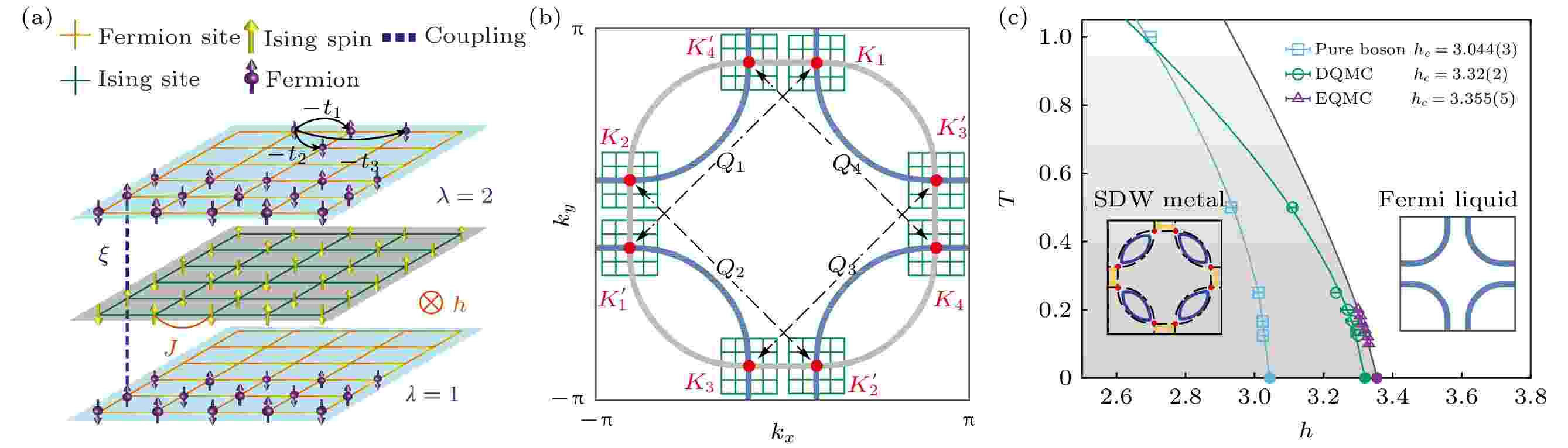
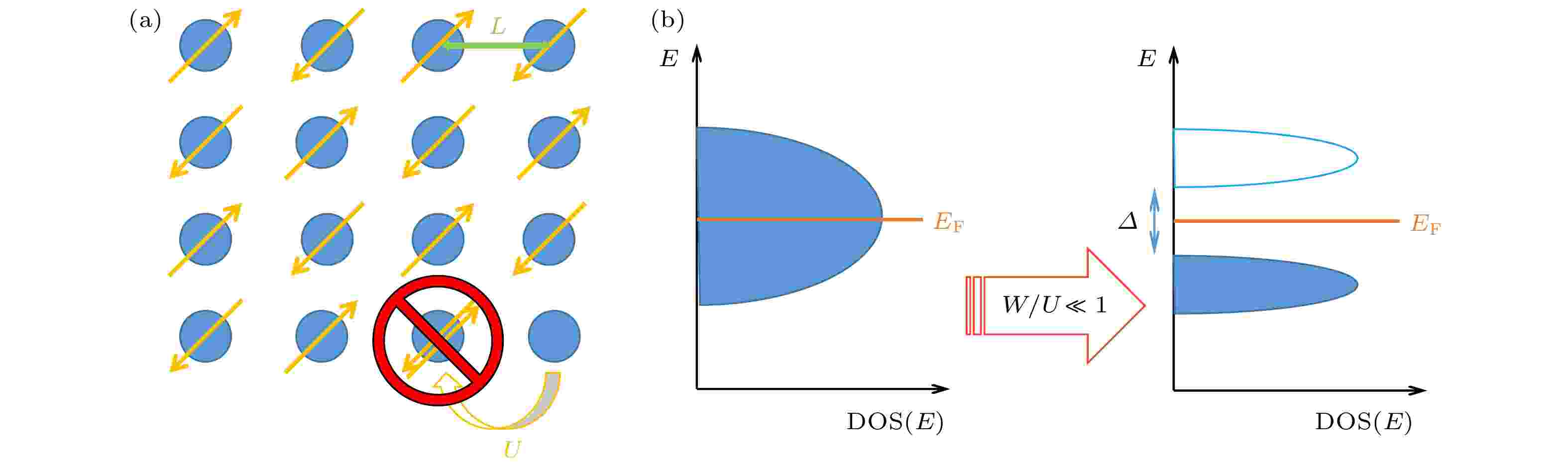
Abstract +
Understanding strongly correlated electrons is an important long-term goal, not only for uncovering fundamental physics behind, but also for their emergence of lots of novel states which have potential applications in quantum control and quantum computations. Meanwhile, the strongly correlated electrons are usually extremely hard problems, and it is generally impossible to understand them unbiasedly. Quantum Monte Carlo is a typical unbiased numeric method, which does not depend on any perturbation, and it can help us to exactly understand the strongly correlated electrons, so that it is widely used in high energy and condensed matter physics. However, quantum Monte Carlo usually suffers from the notorious sign problem. In this paper, we introduce general ideas to design sign problem free models and discuss the sign bound theory we proposed recently. In the sign bound theory, we build a direct connection between the average sign and the ground state properties of the system. We find usually the average sign has the conventional exponential decay with system size increasing, leading to exponential complexity; but for some cases it can have algebraic decay, so that quantum Monte Carlo simulation still has polynomial complexity. By designing sign problem free or algebraic sign behaved strongly correlated electron models, we can approach to several long outstanding problems, such as the itinerant quantum criticality, the competition between unconventional superconductivity and magnetism, as well as the recently found correlated phases and phase transitions in moiré quantum matter.
2022, 71 (12): 127102.
doi: 10.7498/aps.71.20220054
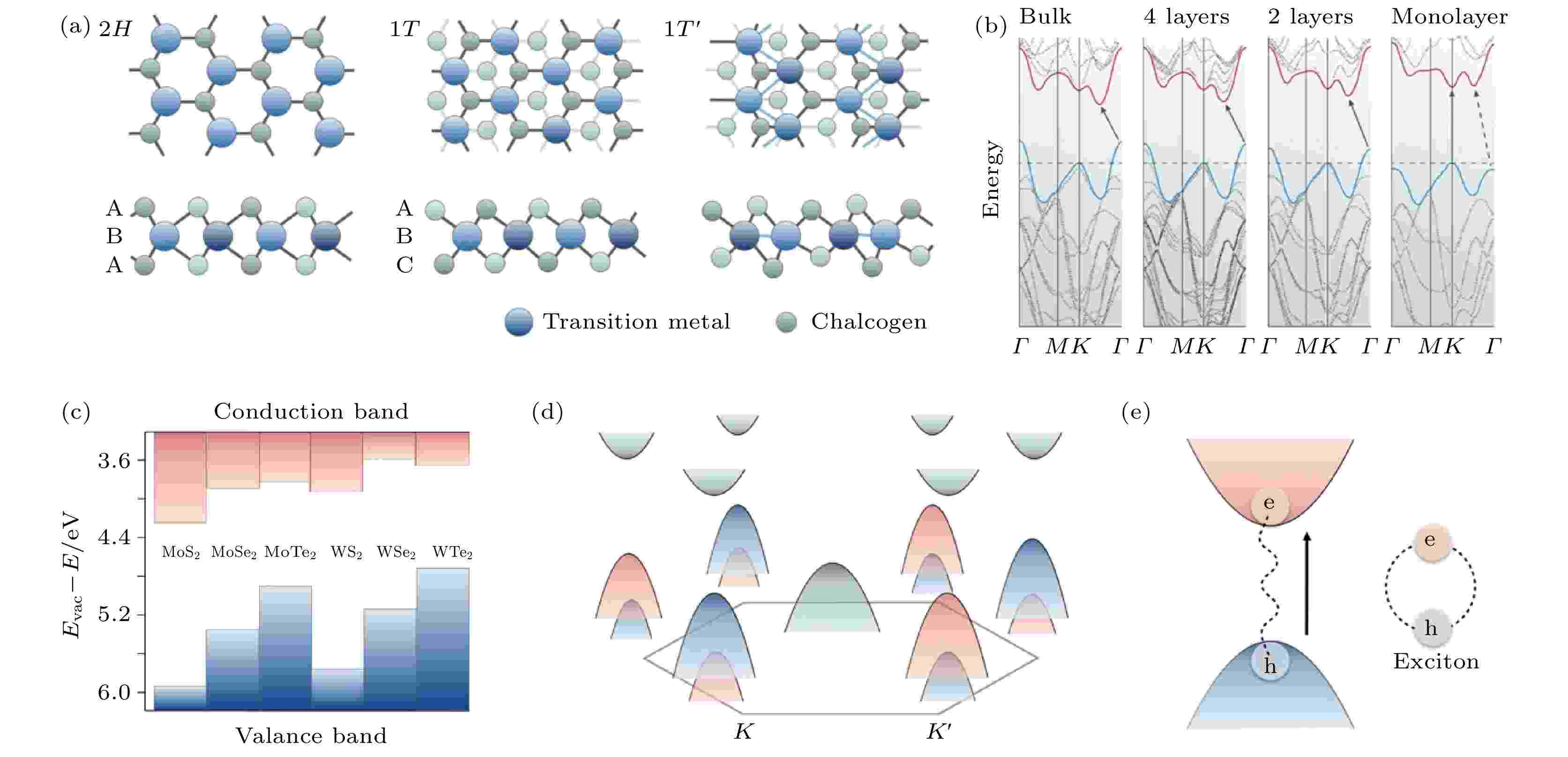
Abstract +
Atomically thin transition metal dichalcogenides (TMDCs) like MX2 (M = W or Mo, X = S or Se) are well-known examples of two-dimensional (2D) semiconductors. They have attracted wide and long-lasting attention due to the strong light-matter interaction and unique spin-valley locking characteristics. In the 2D limit, the reduced dielectric screening significantly enhances the Coulomb interaction. The optical properties of monolayer TMDCs are thus dominated by excitons, the tightly bound electron-hole pairs. In this work, we briefly overview the history and recent research progress of optical spectroscopy studies on TMDCs. We first introduce the layer-dependent band structure and the corresponding modifications on optical transitions, and briefly mention the effects of external magnetic fields and the charge doping on excitons. We then introduce a novel sensing technique enabled by the sensitivity of excitons to the dielectric environment. The exciton excited states (Rydberg states) observed in monolayer TMDCs have large Bohr radii (> few nm), where the electric field lines between electron-hole pairs well extends out of the material. Hence the Coulomb interaction (which affects the quasiparticle band gap and exciton binding energies) in the monolayer TMDC is sensitive to the dielectric environment, making the excitons in 2D semiconductor an efficient quantum sensor in probing dielectric properties of the surroundings. The method is of high spatial resolution and only diffraction limited. We enumerate the applications of monolayer WSe2 dielectric sensor in detecting the secondary Dirac point of graphene induced by the graphene-hBN superlattice potential, as well as the fractional correlated insulating states emerging in WS2/WSe2 moiré superlattices. Meanwhile, a unified framework for describing the many-body interactions and dynamical screenings in the system is still lacking. Future theoretical and experimental efforts are needed for a complete understanding. Finally, we further discuss the perspectives and potential applications of this non-destructive and efficient dielectric sensing method.
2022, 71 (12): 127103.
doi: 10.7498/aps.71.20220052
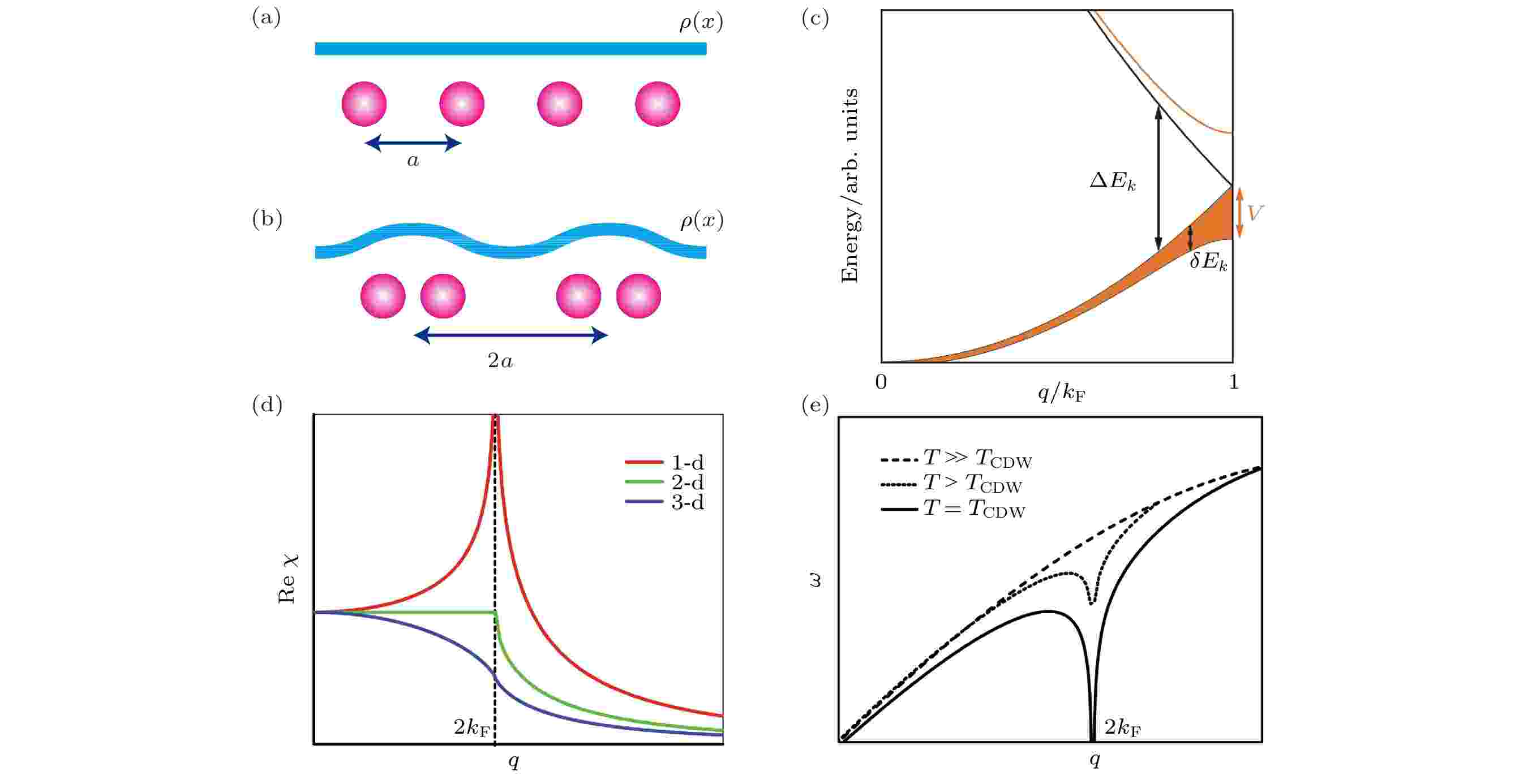
Abstract +
Charge density waves (CDWs) have triggered off extensive research in low-dimensional systems. The discovery of CDW offers a new crucial clue to understanding the intrinsic mechanisms of low-dimensional electron-phonon coupling and electron correlation. In addition, the physical properties of low-dimensional material such as magnetism and superconductivity can be fine-tuned with accurately and effectively controlled CDW phase. At the beginning,we briefly introduce the basic properties of CDW in one-dimensional and quasi one-dimensional materials, revealing the physical proprieties of the CDW, for instance, the excited state and the manipulation technologies. Then, focusing on the CDW in a two-dimensional system, we mainly introduce the recent research progress and the generation mechanism of CDW of two-dimensional materials. The interaction between CDW and Mott insulator and between superconductivity and other orders such as spin density wave and pair density wave provide a new perspective to research the multi-electron collective excitation and electron interaction. The manipulation of multi-electron collective excitation and electron-phonon interaction in CDW through doping, high pressure and laser pulse is also introduced and shares similarity with the one-dimensional system. Finally, in this article we propose a potential research application of two dimensional CDW.
2022, 71 (12): 127104.
doi: 10.7498/aps.71.20220272
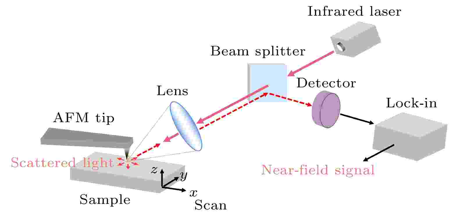
Abstract +
Polaritons, i.e. new collective modes formed by the strong coupling between light and electrons, phonons, excitons, or magnons in matter, have recently received extensive attention. Polaritons in low-dimensional materials exhibit strong spatial confinement, high quality factor, and gate-tunability. Typical examples include gate-tunable graphene surface plasmon polaritons, high-quality hyperbolic phonon polaritons in hexagonal boron nitride, topological phonon polaritons in α-MoO3, and one-dimensional Luttinger-liquid plasmon polaritons in carbon nanotubes. These unique properties make polaritons an excellent candidate for future nano-photonics devices. Further, these polaritons can significantly interact with each other, resulting in a variety of polariton-polariton coupling phenomena, greatly expanding their applications. In this review paper, we first introduce scanning near-field optical microscopy, i.e. the technique used to probe polaritons in low-dimensional materials, then give a brief introduction to the basic properties of polaritons. Next, we discuss in detail the coupling behavior between various polaritons. Finally, potential applications of polaritons coupling are proposed.

2022, 71 (12): 127202.
doi: 10.7498/aps.71.20220064
Abstract +
Two-dimensional (2D) materials can exhibit novel quantum phenomena and be easily tuned by the external environment, which has made them one of the most attractive topics in condensed matter physics during the recent decades. The moiré superlattice induced by varied stacking geometry can further renormalize the material band structure, resulting in the electronic flat bands. With the help of external fields, one can tune the electron-electron correlated interaction in these flat bands, even control the overall physical properties. In this paper we review the recent researches of novel properties in twisted 2D materials (graphene and transition metal dichalcogenide heterostructure), involving strong correlation effect, unconventional superconductivity, quantum anomalous Hall effect, topological phase, and electronic crystals. We also discuss some open questions and give further prospects in this field.
2022, 71 (12): 127302.
doi: 10.7498/aps.71.20220225
Abstract +
In flat bands of two-dimensional materials, the mass of charge carriers increases dramatically and the Coulomb energy of the charge carriers can be much larger than the quenched kinetic energy. When the flat band is partially filled, electron-electron interactions can drive electrons to form exotic correlated phases, such as quantum Hall ferromagnetism, fractional quantum Hall effect, superconductivity, and quantum anomalous Hall effect. Therefore, flat bands in two-dimensional materials have attracted much attention very recently. In the past few years, the strongly correlated phenomena in flat bands have become a hot topic in community of condensed matter physics. There are several different methods, such as using a perpendicular magnetic field, introducing strained structures, and introducing a twist angle, to realize the flat bands in two-dimensional materials. In this review article, we summarize the methods to realize flat bands in two-dimensional systems and introduce the related novel electronic states when the flat band is partially filled.
2022, 71 (12): 127304.
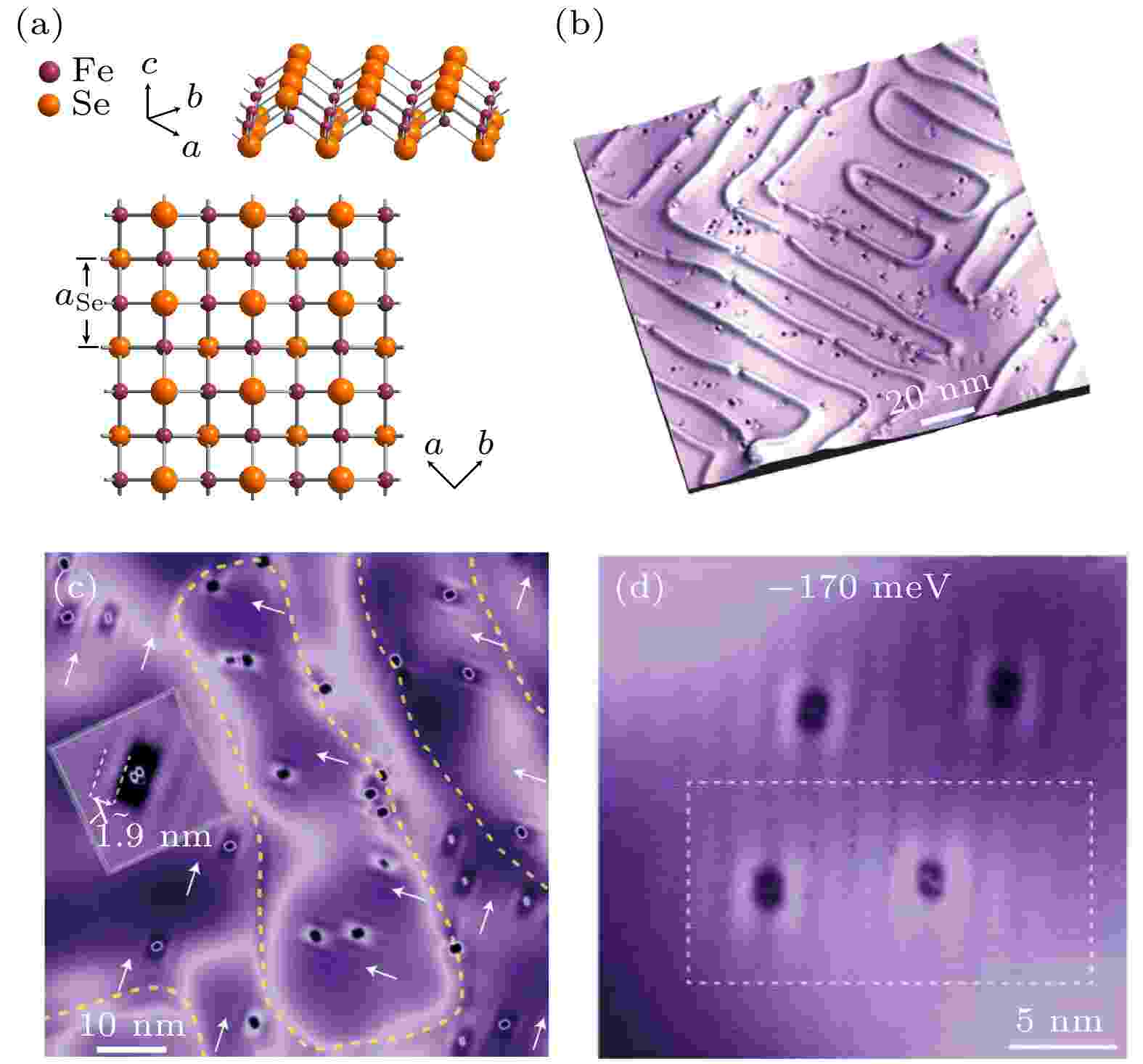
doi: 10.7498/aps.71.20220118
Abstract +
The enhancement of superconductivity in one unit-cell FeSe grown on SrTiO3 is an important discovery in high-temperature superconductivity. In this system, the crucial role of the SrTiO3 substrate has been extensively studied. Its contribution mainly manifests in two aspects: charge transfer and interfacial electron-phonon coupling. However, study of the intrinsic properties of the FeSe thin film itself is still insufficient. In this article, we review the latest research progress of the mechanism of the enhancement of superconductivity in FeSe/SrTiO3, covering the newly discovered stripe phase and its relationship with superconductivity. By using scanning tunneling microscope and molecular beam epitaxy growth method, we find that the electrons in FeSe thin film tend to form stripe patterns, and show a thickness-dependent evolution of short-range to long-range stripe phase. The stripe phase, a kind of electronic liquid crystal state (smectic), originates from the enhanced electronic correlation in FeSe thin film. Surface doping can weaken the electronic correlation and gradually suppress the stripe phase, which can induce superconductivity as well. More importantly, the remaining smectic fluctuation provides an additional enhancement to the superconductivity in FeSe film. Our results not only deepen the understanding of the interfacial superconductivity, but also reveal the intrinsic uniqueness of the FeSe films, which further refines the mechanism of superconductivity enhancement in FeSe/SrTiO3.

2022, 71 (12): 127305.
doi: 10.7498/aps.71.20220349
Abstract +
Ferroelectric (FE) materials possess electrically switchable spontaneous polarizations, showing broad applications in various functional devices. For the miniaturization of electronic devices, two-dimensional (2D) van der Waals (vdW) ferroelectric materials and the corresponding bulk counterparts have aroused more interest of researchers. Recently, several kinds of 2D vdW ferroelectrics have been fabricated in experiment. These 2D vdW FEs, as well as their bulk counterparts, exhibit novel properties as demonstrated in experiment or predicted in theory. This paper is to review the recent progress of novel properties of several vdW ferroelectrics. In Section II, we introduce the unusual ferroelectric property—a uniaxial quadruple potential well for Cu displacements—enabled by the van der Waals gap in copper indium thiophosphate (CuInP2S6). The electric field drives the Cu atoms to unidirectionally cross the vdW gaps, which is distinctively different from dipole reorientation, resulting in an unusual phenomenon that the polarization of CuInP2S6 aligns against the direction of the applied electric field. The potential energy landscape for Cu displacements is strongly influenced by strain, accounting for the origin of the negative piezoelectric coefficient and making CuInP2S6 a rare example of a uniaxial multi-well ferroelectric. In Section III, we introduce the distinct geometric evolution mechanism of the newly reported M2Ge2Y6 (M = metal, X = Si, Ge, Sn, Y = S, Sn, Te) monolayers and a high throughput screening of 2D ferroelectric candidates based on this mechanism. The ferroelectricity of M2Ge2Y6 originates from the vertical displacement of Ge-dimer in the same direction driven by a soft phonon mode of the centrosymmetric configuration. Another centrosymmetric configuration is also dynamically stable but higher in energy than the ferroelectric phase. The metastable centrosymmetric phase of M2Ge2Y6 monolayers allows a new two-step ferroelectric switching path and may induce novel domain behaviors. In Section IV, a new concept about constructing 2D ferroelectric QL-M2O3/graphene heterostructure to realize monolayer-based FE tunnel junctions or potentially graphene p-n junctions is reviewed. These findings provide new perspectives of the integration of graphene with monolayer FEs, as well as related functional devices. Finally, the challenge and prospect of vdW ferroelectrics are discussed, providing some perspective for the field of ferroelectrics.
2022, 71 (12): 127306.
doi: 10.7498/aps.71.20220015
Abstract +
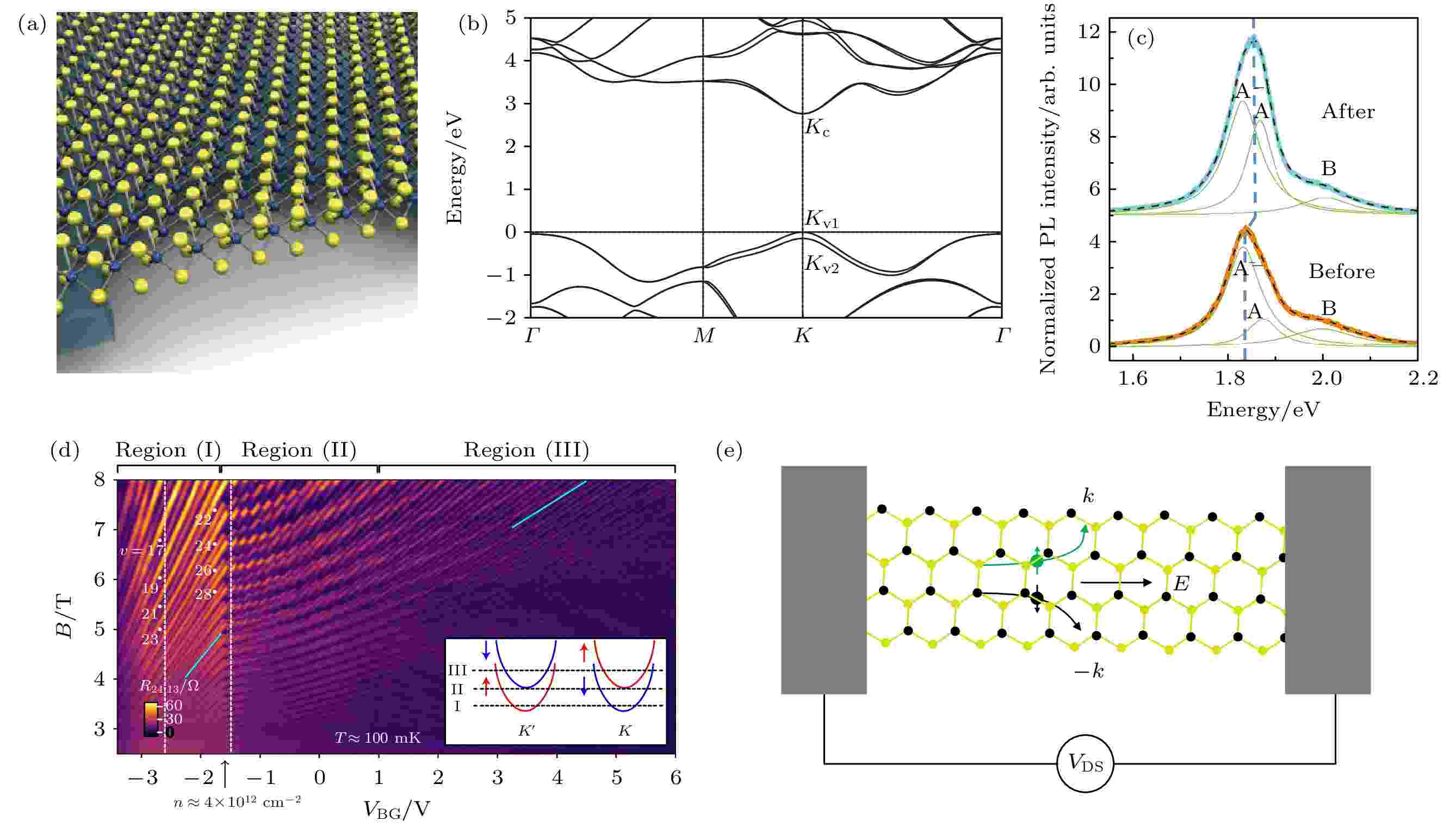
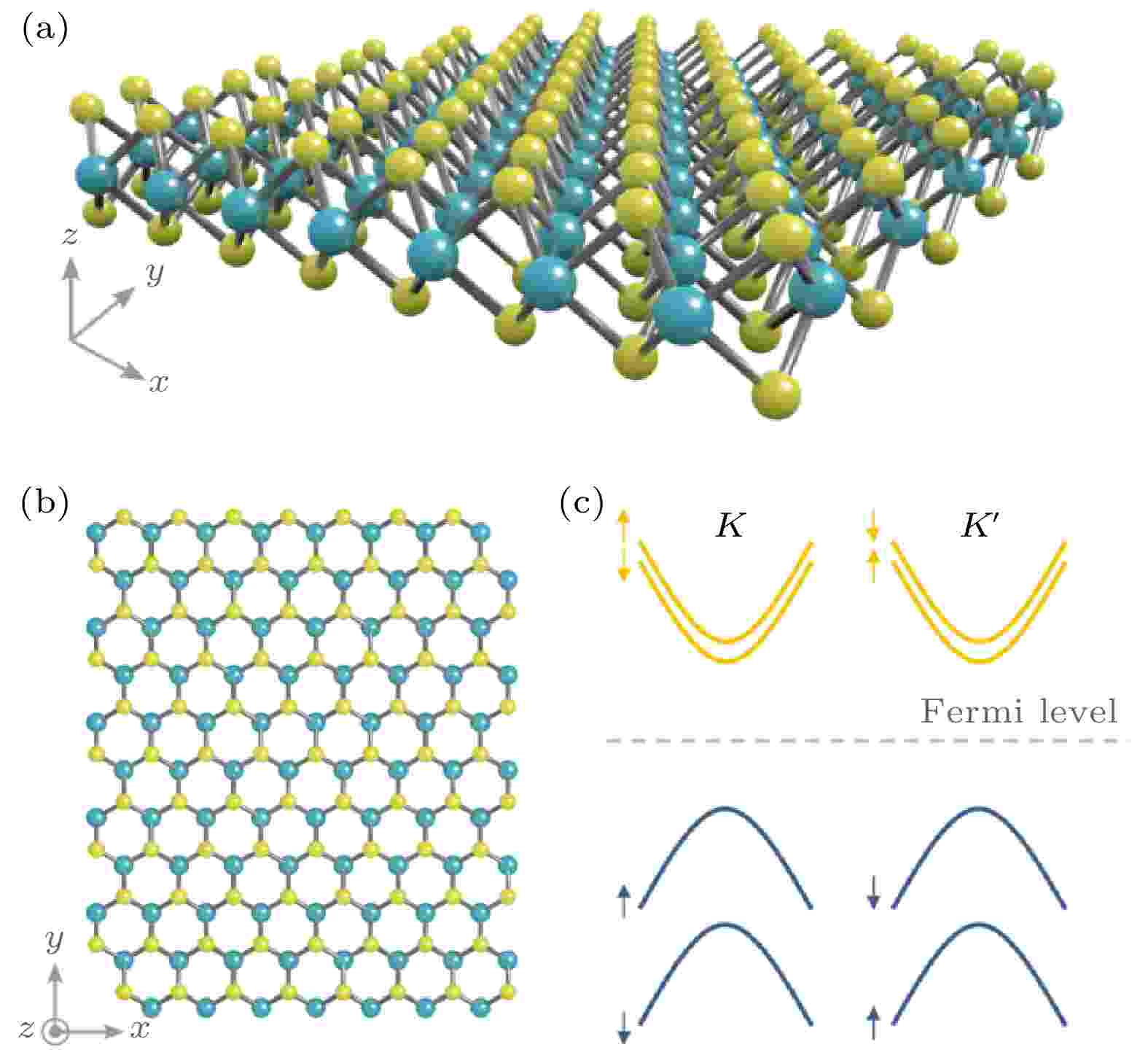
Molybdenum disulfide is a layered transition metal chalcogenide semiconductor. It has many applications in the fields of two-dimensional spintronics, valleytronics and optoelectronics. In this review, molybdenum disulfide is taken as a representative to systematically introduce the energy band structures of single layer, bilayer and twisted bilayer molybdenum disulfide, as well as the latest experimental progress of its realization and low-temperature electrical transport, such as superconductivity and strong correlation phenomenon. Finally, two-dimensional transition metal chalcogenide moiré superlattice’s challenges in optimizing contact and sample quality are analyzed and the future development of this field is also presented.

2022, 71 (12): 127307.
doi: 10.7498/aps.71.20220085
Abstract +
2022, 71 (12): 127308.
doi: 10.7498/aps.71.20220100
Abstract +
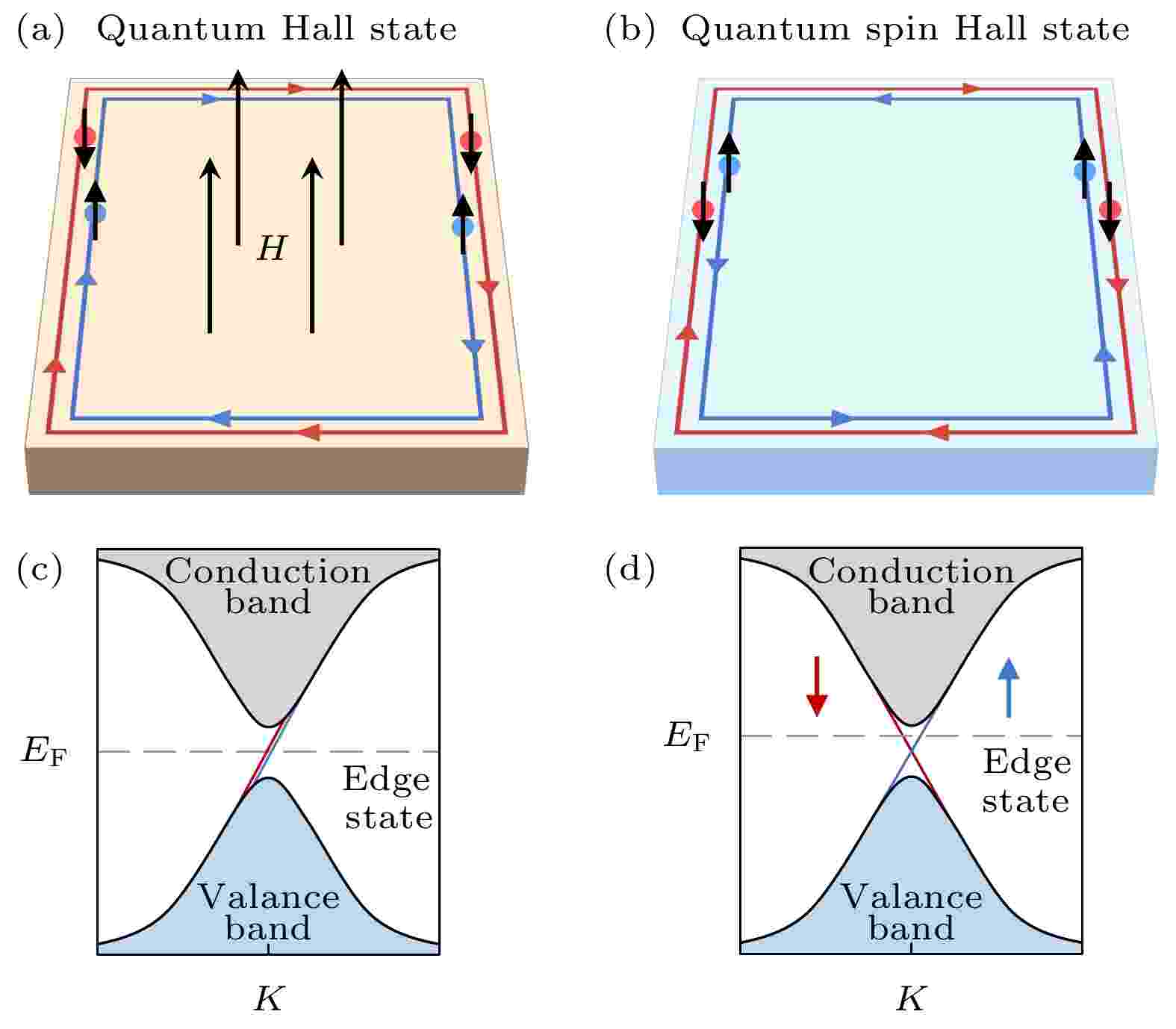
Quantum spin Hall effect, usually existing in two-dimensional (2D) topological insulators, has topologically protected helical edge states. In the year 2014, there was raised a theoretical prediction that monolayer transition metal dichalcogenides (TMDs) with 1T' phase are expected to be a new class of 2D quantum spin Hall insulators. The monolayer 1T'-WTe2 has attracted much attention, because it has various excellent characteristics such as stable atomic structures, an obvious bandgap opening in the bulk of monolayer 1T'-WTe2, and tunable topological properties, which paves the way for realizing a new generation of spintronic devices. In this review, we mainly summarize the recent experimental progress of the 2D quantum spin Hall insulators in monolayer 1T'-WTe2, including the sample preparation via a molecular beam epitaxy technique, the detection of helical edge states and their response on external magnetic fields, as well as the modulation of more rich and novel quantum states under electron doping or strain. Finally, we also prospect the future applications based on monolayer 1T'-WTe2.
2022, 71 (12): 127309.
doi: 10.7498/aps.71.20220347
Abstract +
A moiré superlattice can be formed by overlaying two atomically thin van der Waals materials with a rotation angle or with a lattice mismatch. Since the discovery of correlated insulators and superconductivity in magic angle twisted bilayer graphene, constructing moiré superlattices by various two-dimensional (2D) van der Waals materials and studying their novel properties emerge as a hot topic and research frontier in condensed matter physics. Here we review the recent experimental progress of 2D transition metal dichalcogenide moiré superlattices. In this system, the formation of moiré flat band does not rely on certain magic angles. Experimentally, a series of correlated electron states and topological states have been discovered and confirmed. Further theoretical and experimental studies can find a wealth of emergent phenomena caused by the combined influence of strong correlation and topology in transition metal dichalcogenide moiré superlattice.
2022, 71 (12): 127402.
doi: 10.7498/aps.71.20212289
Abstract +


2022, 71 (12): 127403.
doi: 10.7498/aps.71.20220856
Abstract +
Abundant novel physical properties have been observed in thin-flake samples of two-dimensional correlated electronic systems prepared by mechanical exfoliation. Developing new methods of preparing bulk two-dimensional samples can further understand the low-dimensional system by combining traditional bulk characterization methods like X-ray diffraction, magnetic susceptibility and specific heat measurements. It is possible to maintain the novel properties of thin-flake samples in bulk state and promote these novel physical properties for potential applications. This article introduces a class of organic molecular intercalation methods to regulate two-dimensional correlated electronic systems, focusing on the changes of structure and physical properties of two-dimensional materials after organic molecular intercalation. The applications of organic molecular intercalation method in regulating thermoelectricity, two-dimensional magnetism, charge density wave and two-dimensional superconductivity are also presented.
2022, 71 (12): 127504.
doi: 10.7498/aps.71.20220301
Abstract +
Two-dimensional (2D) magnetic materials with magnetic anisotropy can form magnetic order at finite temperature and monolayer limit. Their macroscopic magnetism is closely related to the number of layers and stacking forms, and their magnetic exchange coupling can be regulated by a variety of external fields. These novel properties endow 2D magnetic materials with rich physical connotation and potential application value, thus having attracted extensive attention. In this paper, the recent advances in the experiments and theoretical calculations of 2D magnets are reviewed. Firstly, the common magnetic exchange mechanisms in several 2D magnetic materials are introduced. Then, the geometric and electronic structures of some 2D magnets and their magnetic coupling mechanisms are introduced in detail according to their components. Furthermore, we discuss how to regulate the electronic structure and magnetism of 2D magnets by external (field modulation and interfacial effect) and internal (stacking and defect) methods. Then we discuss the potential applications of these materials in spintronics devices and magnetic storage. Finally, the encountered difficulties and challenges of 2D magnetic materials and the possible research directions in the future are summarized and prospected.

2022, 71 (12): 127505.
doi: 10.7498/aps.71.20220727
Abstract +
The spontaneous magnetization of two-dimensional (2D) magnetic materials can be maintained down to the monolayer limit, providing an ideal platform for understanding and manipulating magnetic-related properties on a 2D scale, and making it important for potential applications in optoelectronics and spintronics. Transition metal halides (TMHs) are suitable 2D magnetic candidates due to partially filled d orbitals and weak interlayer van der Waals interactions. As a sophisticated thin film growth technique, molecular beam epitaxy (MBE) can precisely tune the growth of 2D magnetic materials reaching the monolayer limit. Moreover, combining with the advanced experimental techniques such as scanning tunneling microscopy, the physical properties of 2D magnetic materials can be characterized and manipulated on an atomic scale. Herein, we introduce the crystalline and magnetic structures of 2D magnetic TMHs, and show the 2D magnetic TMHs grown by MBE and their electronic and magnetic characterizations. Then, the MBE-based methods for tuning the physical property of 2D magnetic TMHs, including tuning interlayer stacking, defect engineering, and constructing heterostructures, are discussed. Finally, the future development opportunities and challenges in the field of the research of 2D magnetic TMHs are summarized and prospected.
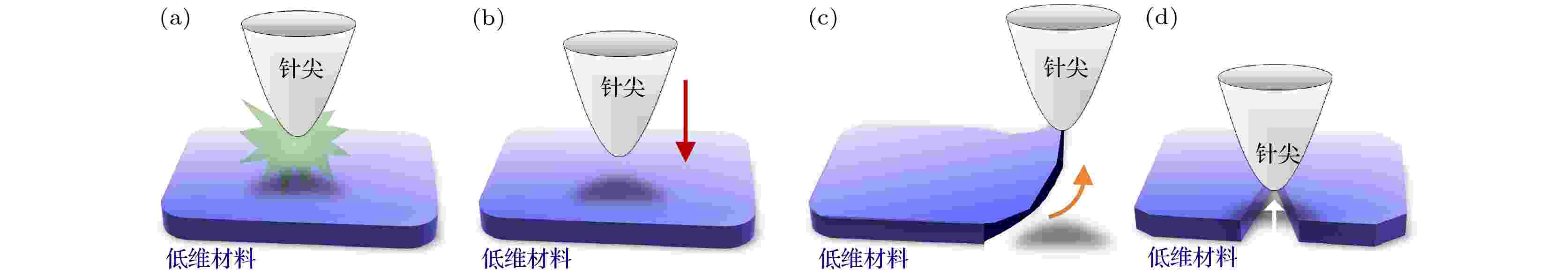
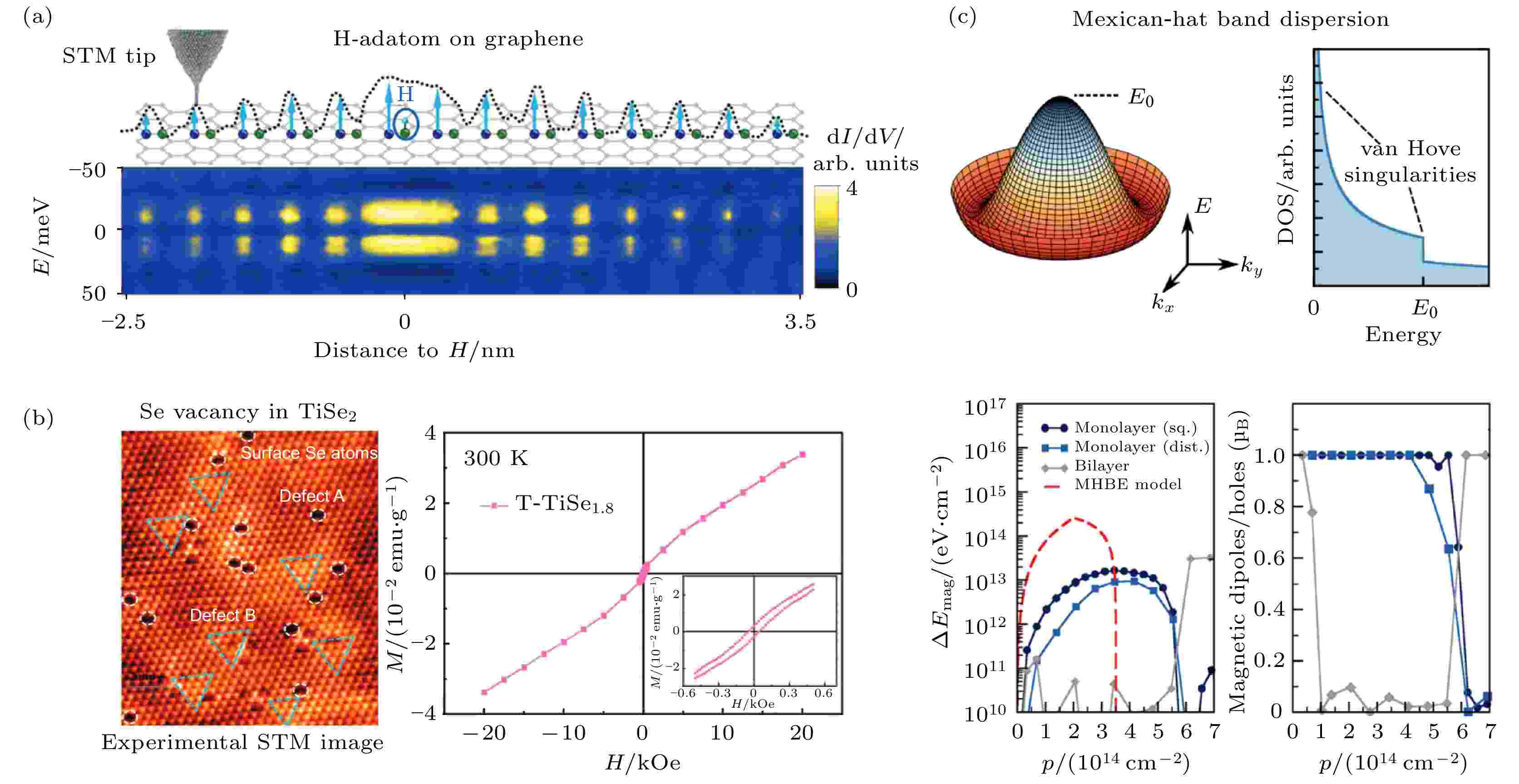
2022, 71 (12): 128102.
doi: 10.7498/aps.71.20220405
Abstract +
Atomic manipulation technique with scanning tunneling microscopy (STM) has been used to control the structural and physical properties of materials at an atomic level. Recently, this technique has been extended to modifying the physical properties of low-dimensional materials. Unlike conventional single atom lateral manipulation, the STM manipulation technique in the study of low-dimensional materials has additional manipulation modes and focuses on the modification of physical properties. In this review paper, we introduce the recent experimental progress of tuning the physical properties of low-dimensional materials through STM atomic manipulation technique. There are mainly four manipulation modes: 1) tip-induced local electric field; 2) controlled tip approach or retract; 3) tip-induced non-destructive geometry manipulation; 4) tip-induced kirigami and lithography. Through using these manipulation modes, the STM tip effectively introduces the attractive force or repulsive force, local electronic field or magnetic field and local strain, which results in the atomically precise modification of physical properties including charge density wave, Kondo effect, inelastic tunneling effect, Majorana bound states, and edge states.
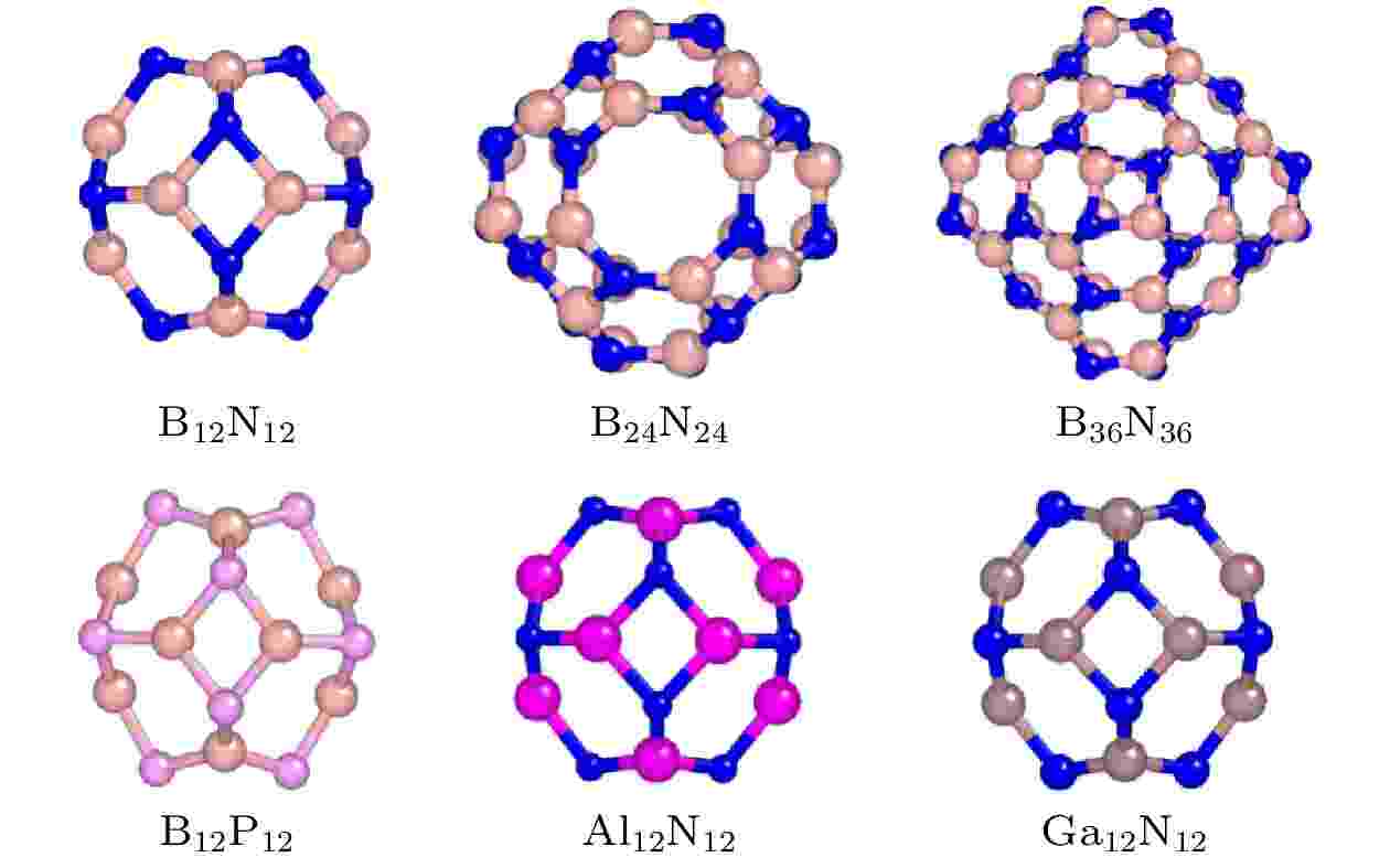
2022, 71 (12): 123601.
doi: 10.7498/aps.71.20212426
Abstract +
Thermally activated delayed fluorescence (TADF), a unique molecular fluorescence mechanism, plays a key role in designing emitters of high efficiency. Carbon fullerenes such as C60 and C70 exhibit strong TADF with intensity even higher than that of the prompt fluorescence, owing to their long lifetimes of triplet state and modest singlet-triplet energy gaps. Thus, there arises the intriguing question whether other fullerene-like clusters can also have fluorescence and host the TADF effect. In this work, by time-dependent density functional theory (TD-DFT) calculations, we explore the excited-states of the experimentally reported boron nitride cage clusters B12N12, B24N24 and B36N36, as well as compound clusters B12P12, Al12N12 and Ga12N12 with the same geometry as B12N12. Using the HSE06 hybrid functional, the predicted energy gaps of these fullerene-like clusters are obtained to range from 2.83 eV to 6.54 eV. They mainly absorb ultraviolet light, and their fluorescence spectra are all in the visible range from 405.36 nm to 706.93 nm, including red, orange, blue, and violet emission colors. For the boron nitride cages, the energy gap of excited states increases with the cluster size increasing, accompanied by a blue shift of emission wavelength. For the clusters with B12N12 geometry and different elemental compositions, the excited energy gap decreases as the atomic radius increases, resulting in a red shift of emission wavelength. In addition, the highest occupied molecular orbitals (HOMOs) and lowest unoccupied molecular orbitals (LUMOs) of these compound cage clusters are distributed separately on different elements, resulting in small overlap between HOMO and LUMO wavefunctions. Consequently, these fullerene-like clusters exhibit small singlet-triplet energy differences below 0.29 eV, which is beneficial for the intersystem crossing between the excited singlet state and triplet state, and hence promoting the TADF process. Our theoretical results unveil the fluorescence characteristics of cage clusters other than carbon fullerenes, and provide important guidance for precisely modulating their emission colors by controlling the cluster sizes and elemental compositions. These experimentally feasible fullerene-like compound clusters possess many merits as fluorophors such as outstanding stabilities, non-toxicity, large energy gap, visible-light fluorescence, and small singlet-triplet energy gap. Therefore, they are promising luminescent materials for applications in display, sensors, biological detection and labelling, therapy, and medicine.
2022, 71 (12): 127203.
doi: 10.7498/aps.71.20220029
Abstract +
Graphene, a special two-dimensional material, has a unique band structure that allows the type and concentration of carriers to be controlled through a gate voltage, and it has potential applications in bipolar nanoelectronic devices. In this paper, based on the tight-binding model of graphene p-n junctions, by using the nonequilibrium Green’s function method and Landauer-Büttiker formula, the thermal dissipation of electric transport in graphene p-n junctions in a magnetic field is investigated. Under a strong magnetic field, both sides of the junction are in the quantum Hall regime, thus the topologically protected chiral edge states appear. Intuitively, the topologically protected chiral edge states are dissipationless. However, the results show that thermal dissipation can occur in the quantum Hall regime in graphene junctions in the presence of dissipation sources, although the topologically protected chiral edge states still exist. In clean graphene junctions, thermal dissipation occurs mainly at the edge for the unipolar transport, but it occurs both at the edge and at the interface of the junctions for the bipolar transport. In the presence of disorder, thermal dissipation is significantly enhanced both in the unipolar junction and in the bipolar junction, and it increases with disorder strength increasing. Besides, the energy distribution of electrons at different positions is also studied, which shows that the thermal dissipation always occurs as long as the energy distribution is in nonequilibrium. This indicates that the topology can protect only the propagation direction of electrons, but it can not suppress the occurrence of thermal dissipation.
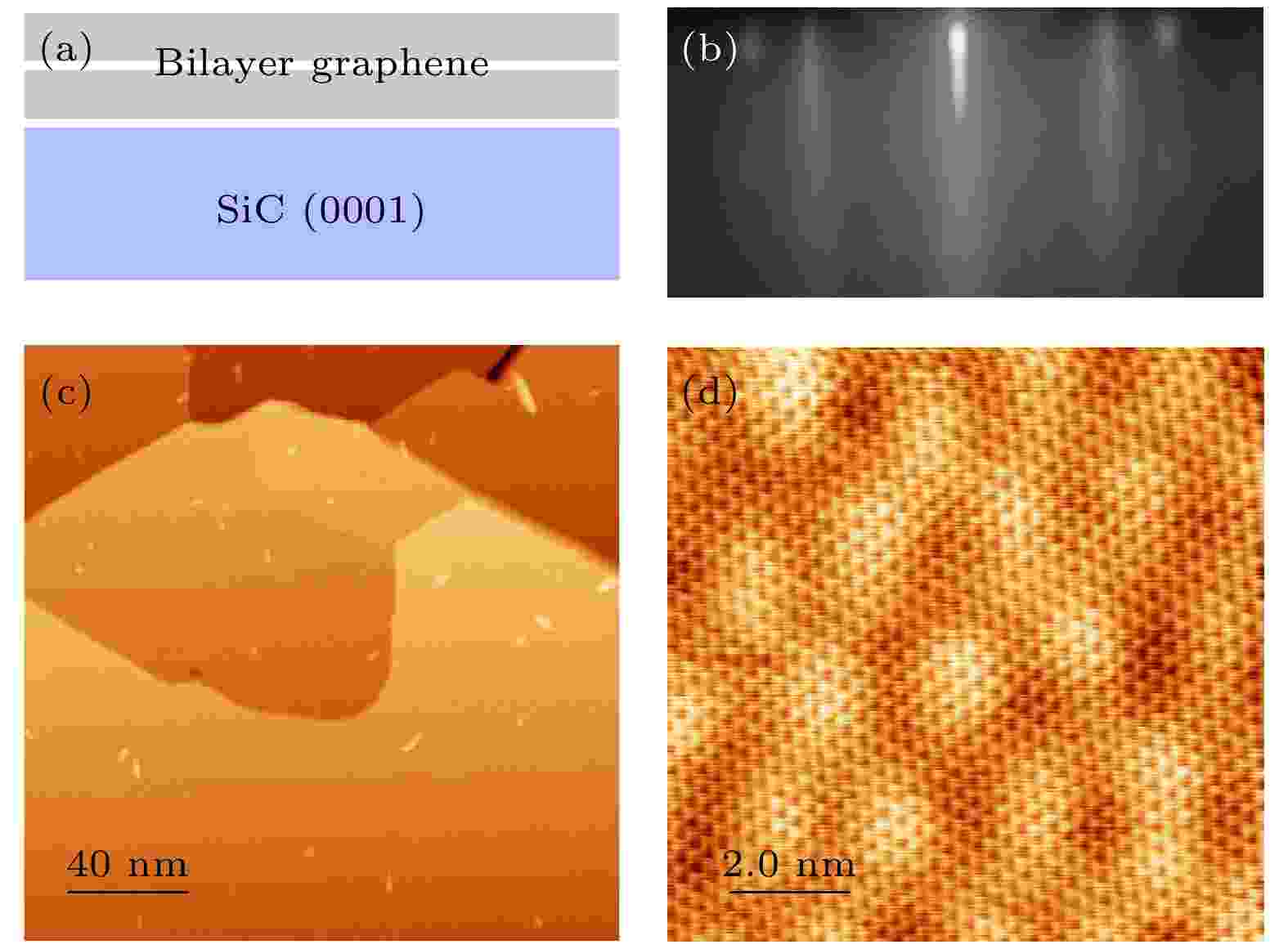
2022, 71 (12): 127204.
doi: 10.7498/aps.71.20220062
Abstract +
Graphene can find great potential applications in the future electronic devices. In bilayer graphene, the relative rotation angle between graphene layers can modulate the interlayer interaction and hence induces rich physical phenomena. We systematically study the temperature dependent magnetoresistance (MR) properties in the epitaxial bilayer graphene (BLG) grown on the SiC substrate. High quality BLG is synthesized by molecular beam epitaxy in ultra-high vacuum. We observe the negative MR under a small magnetic field applied perpendicularly at temperature < 80 K, which is attributed to a weak localization effect. The weak localization effect in our epitaxial BLG is stronger than previously reported ones in epitaxial monolayer and multilayer graphene system, which is possibly because of the enhanced interlayer electron transition and thus the enhanced valley scattering in the BLG. As the magnetic field increases, the MR exhibits a classical Lorentz MR behavior. Moreover, we observe a linear magnetoresistance behavior in a large field, which shows no saturation for the magnetic field of up to 9 T. In order to further investigate the negative and linear magnetoresistance, we conduct angle-dependent magnetoresistance measurements, which indicates the two-dimensional magnetotransport phenomenon. We also find that the negative MR phenomenon occurs under a parallel magnetic field, which may correspond to the moiré pattern induced local lattice fluctuation as demonstrated by scanning tunneling microscopy measurement on an atomic scale. Our work paves the way for investigating the intrinsic properties of epitaxial BLG under various conditions.
2022, 71 (12): 127303.
doi: 10.7498/aps.71.20220246
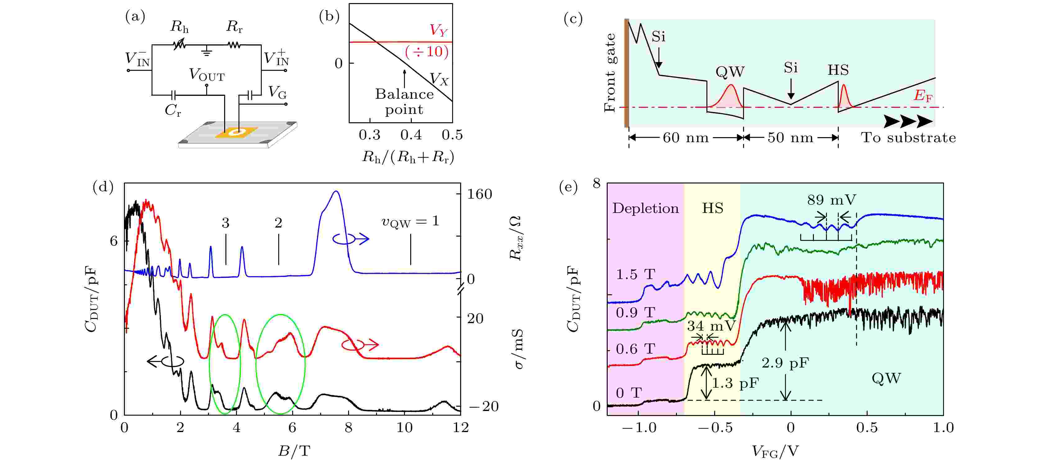
Abstract +
We introduce two contactless measurement methods at extremely low temperature: capacitances and surface acoustic waves. Both methods can be used to study the physical properties of the quantum system through the interaction between electrons and high frequency electric field. We first present preliminary results of high-mobility two-dimensional electron systems studied by a high-precision capacitance measurement method at extremely low temperature. Our setup can resolve < 0.05% variation of a < 1 pF capacitance at 10 mK–300 K and 0–14 T. Second, we also study two-dimensional electron systems using surface acoustic waves. We can use 0.1 nW excitation and obtain < 10–5 sensitivity. These measurement methods may be widely applied to the study of two-dimensional systems, especially the materials without high quality contacts.
COVER ARTICLE
2022, 71 (12): 127401.
doi: 10.7498/aps.71.20220050
Abstract +
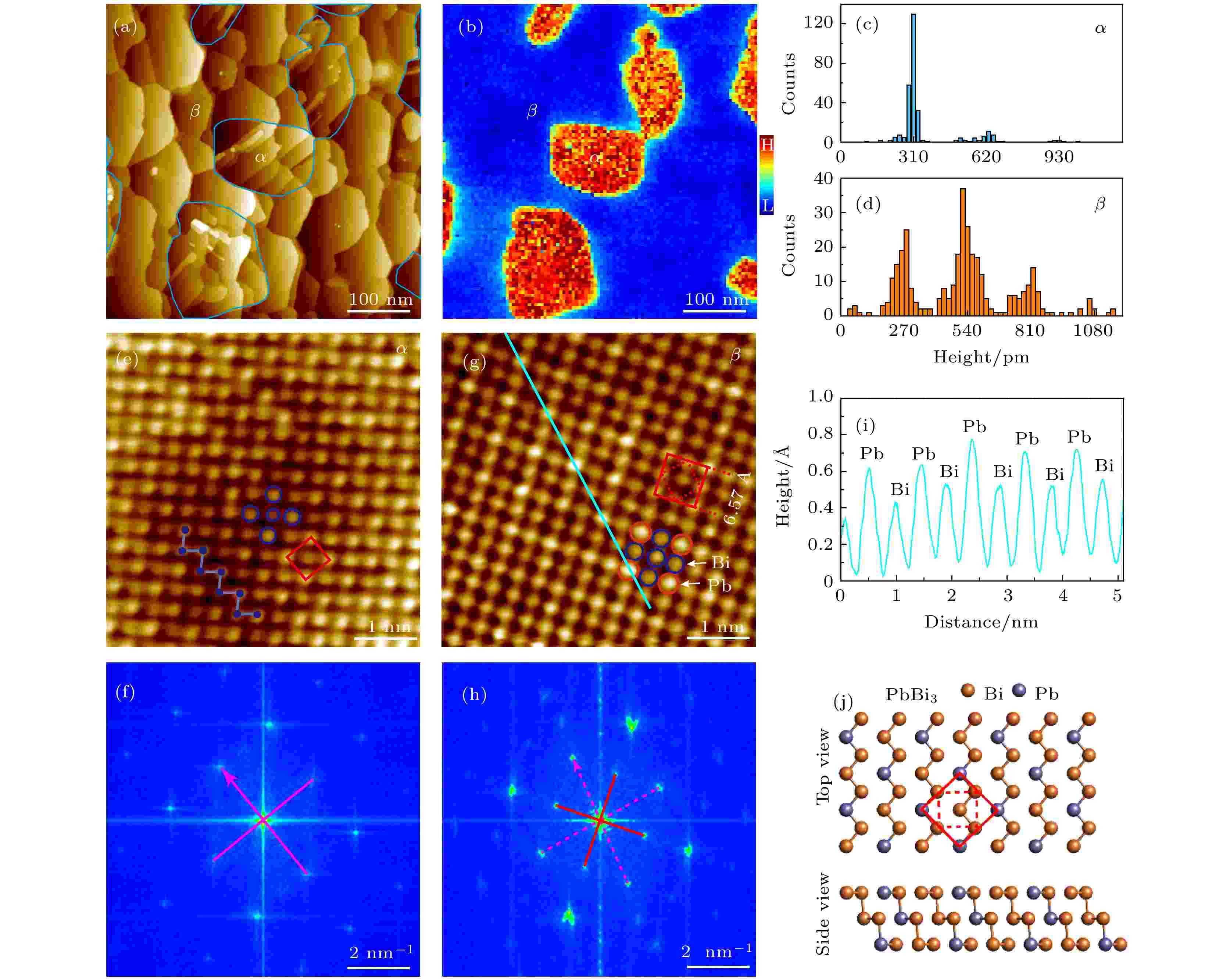
Bismuth (Bi), as a stable heaviest element in the periodic table of elements, has strong spin-orbit coupling, which has attracted a lot of attention as the parent material of various known topological insulators. Previous calculations predicted that Bi(111) with a thickness less than eight bilayers and the ultrathin black-phosphorus-like Bi(110) films are single-element two-dimensional (2D) topological insulators. However, it is generally believed that these crystalline bismuth phases are not superconducting or their transition temperature should be lower than 0.5 mK. Lead (Pb) is a good superconducting elementary material, and there is a relatively small difference in radius between the Bi atom and Pb atom. According to the Hume-Rothery rule, it is expected that Pb/Bi alloys in an arbitrary ratio should be superconducting. One may thus expect to form crystalline Bi based superconductors by Pb substitution, which might host intriguing topological superconductivity. While our previous work has demonstrated a low-temperature stable Pb1–xBix (x~0.1) alloy phase in which Pb in the Pb(111) structure is partially replaced by Bi, the Bi crystalline structure-based phases of the superconducting alloys still lack in-depth research. Here, we report a new low-temperature phase of Pb-Bi alloy thin film, namely PbBi3, on the Si(111)-(7 × 7) substrate, by co-depositing Pb and Bi at a low temperature of about 100 K followed by an annealing treatment of 200 K for 2 h. Using low-temperature scanning tunneling microscopy and spectroscopy (STM/STS), we characterize in situ the surface structure and superconducting properties of the Pb-Bi alloy film with a nominal thickness of about 4.8 nm. Two spatially separated phases with quasi-tetragonal structure are observed in the surface of the Pb-Bi alloy film, which can be identified as the pure Bi(110) phase and the PbBi3 phase, respectively, based on their distinct atomic structures, step heights and STS spectra. The PbBi3 film has a base structure similar to Bi(110), where about 25% of the Bi atoms are replaced by Pb, and the surface shows a $\sqrt 2 \times \sqrt 2 R{45^ \circ }$ reconstructed structure. The superconducting behavior of the PbBi3 phase is characterized using variable-temperature STS spectra. We obtain that the superconducting transition temperature of PbBi3 is about 6.13 K, and the $2\varDelta (0)/{k_{\text{B}}}{T_{\text{c}}}$ ratio is about 4.62 using the fitting parameter of $\varDelta (0) = 1.22{\text{ meV}}$ at 0 K. By measuring the magnetic field dependent superconducting coherence length, the critical field is estimated at larger than 0.92 T. We further investigate the superconducting proximity effect in the normal metal-superconductor (N-S) heterojunction consisting of the non-superconducting Bi(110) domain and the superconducting PbBi3 domain. The N-S heterojunctions with both in-plane configuration and step-like configuration are measured, which suggest that the atomic connection and the area of the quasi-2D Josephson junctions and the external magnetic field can affect the lateral superconducting penetration length. We also observe the zero-bias conductance peaks (ZBCPs) in the superconducting gap of the PbBi3 surface in some cases at zero magnetic field. By measuring dI/dV spectra at various temperatures and by adopting a superconducting Nb tip, we identify that the ZBCP originates from the superconductor-insulator-superconductor (S-I-S) junction formed between a superconducting tip and the sample. Nevertheless, the Bi(110)-based PbBi3 phase may provide a possible platform to explore the intriguing topological superconducting behaviors at the vortexes under magnetic fields, or in the vicinity of the potentially topological superconducting Bi(110) islands by considering the proximity effect.


2022, 71 (12): 127503.
doi: 10.7498/aps.71.20220699
Abstract +
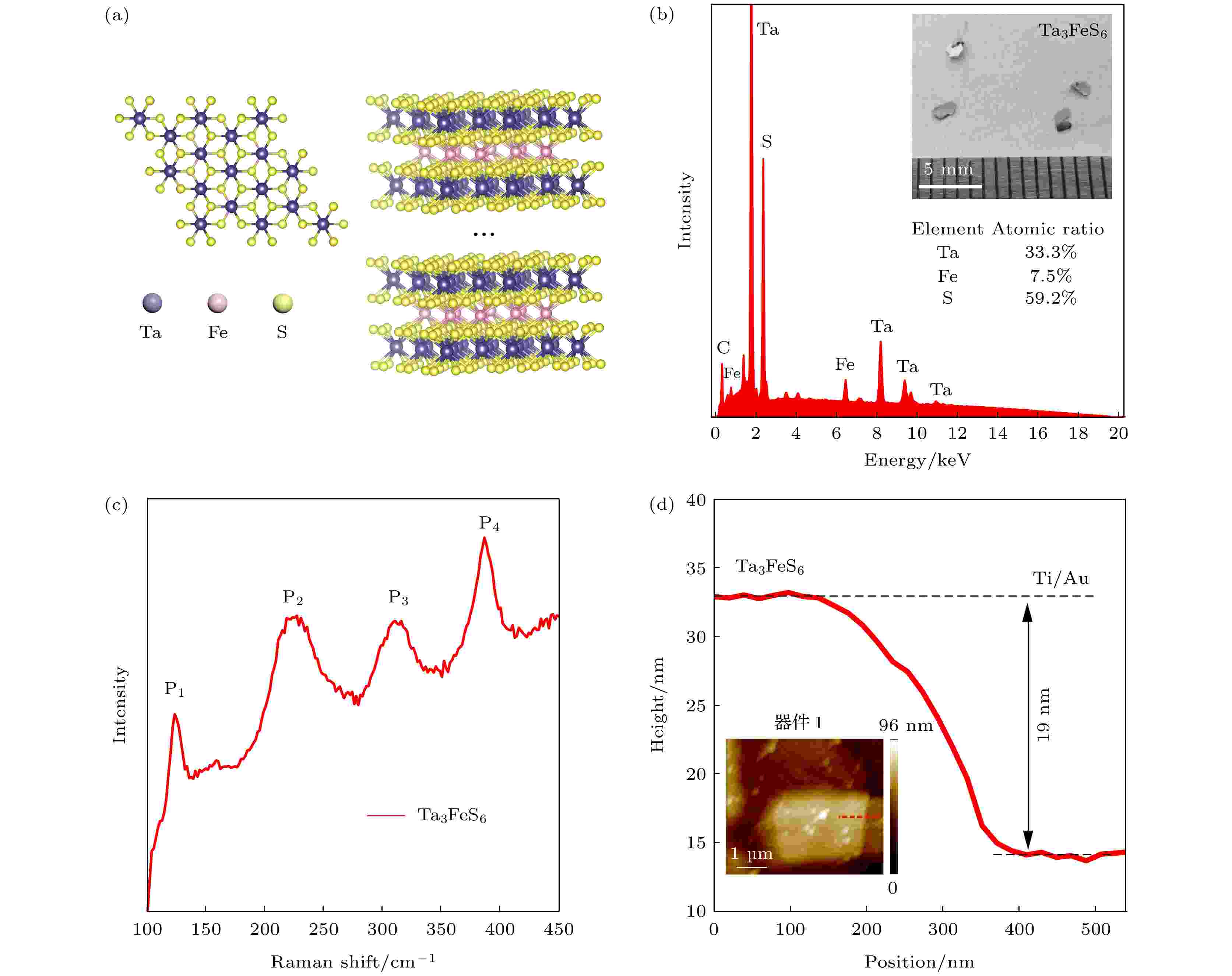
Van der Waals (vdW) layered ferromagnetic materials provide a unique platform for fundamental spintronic research, and have broad application prospects in the next-generation spintronic devices. In this study, we synthesize high-quality single crystals of vdW intrinsic ferromagnet Ta3FeS6 by the chemical vapor transport method. We obtain thin layer samples of Ta3FeS6 with thickness values ranging from 19 to 100 nm by the mechanical exfoliation method, and find that their corresponding Curie temperatures are between 176 and 133 K. The anomalous Hall measurement shows that the Ta3FeS6 has out-of-plane ferromagnetism with the coercivity reaching 7.6 T at 1.5 K, which is the largest value in those of the layered vdW ferromagnetic materials reported so far. In addition, we observe that the reversal polarity of the hysteresis loop changes sign with temperature increasing. Our work provides an opportunity to construct stable and miniaturized spintronic devices and present a new platform for studying spintronics based on van der Waals magnetic materials.

2022, 71 (12): 127901.
doi: 10.7498/aps.71.20220458
Abstract +
Transition metal dichalcogenides (TMDs) have attracted a lot of interest in condensed matter physics research due to the existence of multiple novel physical phenomena, including superconductivity and charge density wave order, and also TMDs provide a unique window for studying the interactions between different ground states. In this work, the electronic structure of 1T-NbSeTe is systematically examined by angle-resolved photoemission spectroscopy (ARPES) for the first time. A van Hove singularity (VHS) is identified at the M point, with binding energy of 250 meV below the Fermi level. Careful analysis is carried out to examine the band dispersions along different high symmetry directions and the possible many-body effect. However, the dispersion kink—a characteristic feature of electron-boson coupling is not obvious in this system. In TMD materials, the van Hove singularity near the Fermi level and the electron-boson (phonon) coupling are suggested to play an important role in forming charge density wave (CDW) and superconductivity, respectively. In this sense, our experimental results may provide a direct explanation for the weakened CDW and relatively low superconducting transition temperature in 1T-NbSeTe. These results may also provide an insight into the charge-density-wave orders in the relevant material systems.

2022, 71 (12): 128103.
doi: 10.7498/aps.71.20220132
Abstract +
Among two-dimensional (2D) materials, transition metal chalcogenides (TMDs) have attracted much attention due to their unique photoelectric properties. On the other hand, organic molecules have the characteristics of flexibility, wide source, easy fabrication and low cost. The van der Waals heterostructure constructed by the combination of 2D TMDs and organic semiconductors has attracted enormous attention in recent years. When organic semiconductors combine with TMDs to form van der Waals heterostructure, the hybridization of organic molecules could improve the photoelectric properties and other properties by taking the advantages of these two materials, Therefore, the combination of organic semiconductor molecules and TMDs can provide a research platform for designing many basic physics and functional devices and interesting optoelectronic applications. In this work, CuPc/MoS2 van der Waals heterostructure is built, and its photoluminescence (PL) properties are investigated. It is observed that after introducing CuPc, a significant PL quenching phenomenon occurs in the heterostructure compared with the single layer MoS2 and pure CuPc only. After fitting the PL of CuPc/MoS2 heterostructure system and monolayer MoS2 only, the ratio of trion to neutral exciton is clearly increased in the heterostructure. Furthermore, it is found that two mid-gap states D1 and D2 related to the CuPc are introduced into the band gap of MoS2 by first principle calculation. Through the charge density analysis, we find that the D1 state originates from the sp2 bonding state of the C-C bond while the D2 state comes from the anti-bonding state of the N-Cu bond. Meanwhile, the valence band maximum (VBM) and conduction band minimum (CBM) of CuPc/MoS2 heterostructure are derived from the bonding and anti-bonding states of MoS2, respectively. The charge transfer occurs between the mid-gap states of CuPc and MoS2. However, owing to different positions of charge density distribution of CBM, D2, D1 and VBM, the charge pathway is dominated by non-radiation recombination, which cannot give new PL peak in heterostructure. However, this process reduces the number of carriers involved in the direct recombination of MoS2, which leads PL to quench in the heterostructure. This work would be applied to the manipulation of photoelectric characteristics and the design of TMD/organic-based photovoltaic applications.
2022, 71 (12): 128104.
doi: 10.7498/aps.71.20220273
Abstract +
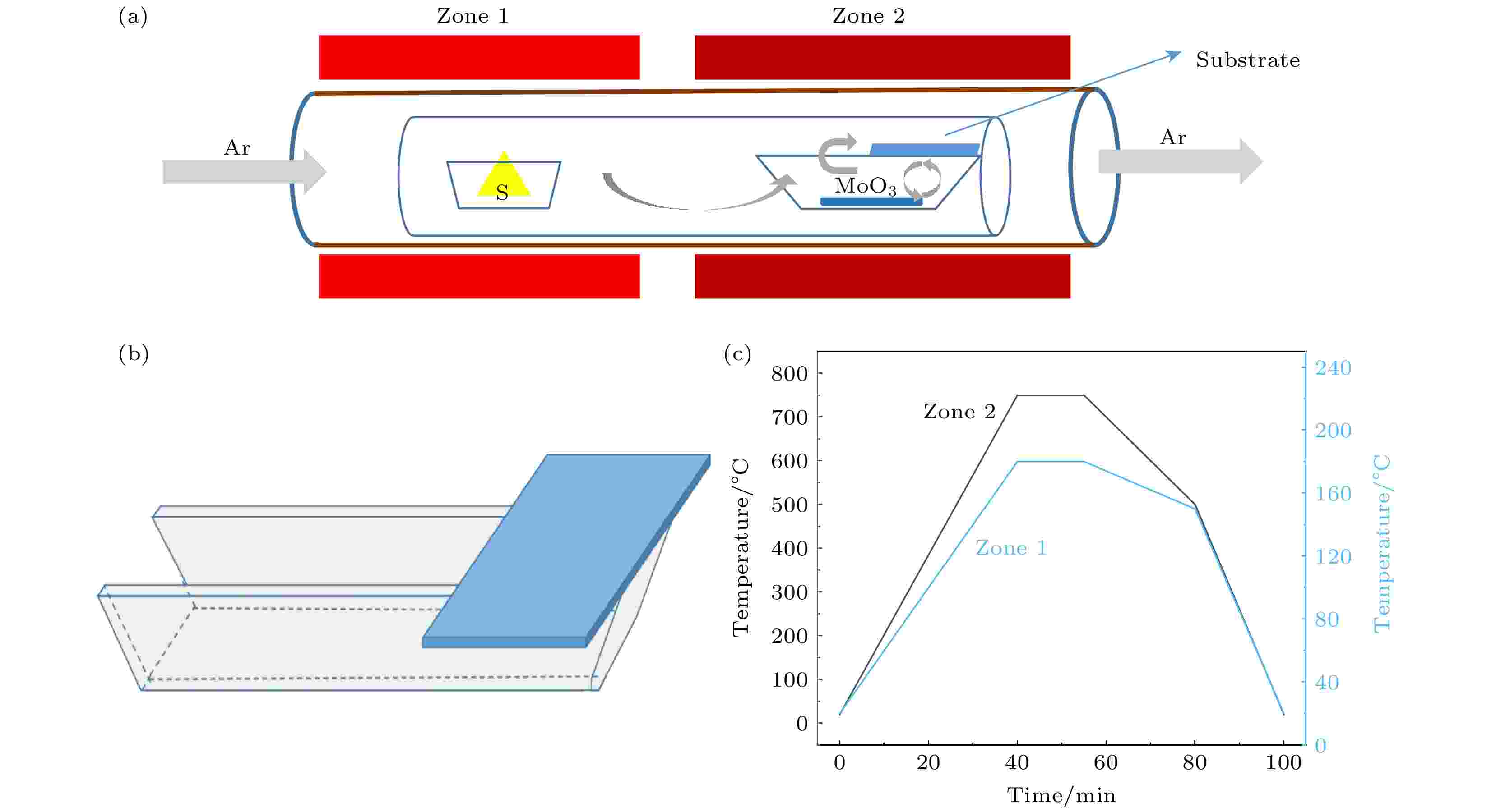
In recent years, transition metal dichalcogenides materials represented by monolayer molybdenum disulfide (MoS2) have aroused great interest due to their excellent optical and electrical properties. The synthesis method of high-quality monolayer MoS2 film is a key problem for scientific research and industrial application. Recently, researchers have proposed a salt-assisted chemical vapor deposition method for growing the monolayer films, which greatly promotes the growth rate and quality of monolayer film. By using this method, we design a growth source of semi-enclosed quartz boat, and successfully obtain high-quality monolayer MoS2 films by using the double auxiliary action of sodium chloride (NaCl). Scanning electron microscopy shows the excellent film formation, and the photoluminescence spectra show that the luminescence intensity is significantly higher than that of the sample grown without NaCl. The NaCl double-assisted growth method proposed in this study can reduce the growth temperature of MoS2, shorten the growth time, and improve the optical properties of the films. Besides, the operation is simple and the cost is low, which provides an idea for growing the large-scale two-dimensional materials.
REVIEW
2022, 71 (12): 126801.
doi: 10.7498/aps.71.20220215
Abstract +
The resonant sensor is a kind of high-sensitivity and high-stability sensor that directly outputs digital signals. The resonance sensitive elements of traditional resonant sensors are mostly made of metal, quartz crystal, silicon and other materials. However, with the development of resonant sensor toward the miniaturization and intellectualization, the sensitive materials of new resonator are micro-nano machined and highly sensitive. As a new type of two-dimensional nanomaterial, graphene has the great potentials in the field of resonance sensing because of its excellent mechanical, electrical, optical and thermal properties. Therefore, the mechanical quantity sensor based on graphene material is expected to surpass the silicon material mechanical quantity sensor in many aspects such as micro-nano size, high performance, and environmental adaptability. This review focuses on the graphene resonant mechanical quantity sensor. In the first part, we summarize the basic properties, preparation methods, and transfer methods of graphene materials. The preparation and transmission methods of graphene are key to high-performance graphene resonator, but there are still different problems in the preparation and transfer of graphene, which also greatly restricts the development of graphene resonator. In the second part, the basic theory of resonant sensors is given, and the common methods of transferring graphene films are introduced in detail. Then the theoretical and experimental studies of graphene resonator are discussed. For example, the theoretical studies of graphene resonator are investigated by using the classical elastic theory, non-local elastic theory, molecular structure mechanics and molecular dynamics. Then the effects of graphene preparation method, graphene layer number and shape, excitation and detection methods on the resonance performance are estimated in the resonant experiments of graphene resonators. After that, the research progress of graphene resonator is summarized in the fields of pressure, acceleration and mass sensors. Compared with traditional silicon resonators, graphene resonators have a small dimension and demonstrate preferable resonant performance under low-temperature and low-pressure conditions. In this case, the technical issues of graphene resonant sensor are introduced to emphasize the importance of suspended graphene film transfer, structure fabrication of harmonic oscillator and vibration excitation/detection of resonators, which contributes to the potential applications in the fields of aerospace, intelligent detection and biomedical sensing for graphene resonant sensors.
GENERAL
2022, 71 (12): 120701.
doi: 10.7498/aps.71.20220150
Abstract +
Nitrous acid (HONO), as an important precursor of hydroxyl (OH) radical, has a low concentration, short lifetime, easy loss and high reactivity in the atmosphere. Thus, the high sensitivity detection of atmospheric HONO is a challenge. In this paper, we report an open-path broadband cavity enhanced absorption spectroscopy (OP-BBCEAS) system based on the iterative algorithm for simultaneous measurement of atmospheric HONO and NO2. In the conventional BBCEAS system, a pump is used to drive the ambient air into the optical cavity through the filter membrane for measurement, which can reduce the influence of aerosol particle extinction. However, the influence of wall loss and secondary formation caused by the optical cavity and sampling should be considered for reactive component measurements. The OP-BBCEAS with open-path configuration is adopted in this paper to avoid being influenced by wall effect. The effective absorption optical path is calculated by the iterative retrieval algorithm through multiple iterations, and the absorption of HONO and NO2 are then quantified by the spectral fitting method of differential optical absorption spectroscopy, which removes the broadband change influence of the Mie scattering extinction by aerosol particles and the light intensity fluctuation. The atmospheric HONO and NO2 with light (PM2.5 < 75 μg/m3) and moderate (PM2.5 > 75 μg/m3) aerosol loading are measured by the OP-BBCEAS system based on iterative algorithm, and compared with the counterparts by the conventional close-path BBCEAS system. The concentrations of HONO and NO2 measured by the two BBCEAS systems are in good agreement (R2 > 0.99) for different PM2.5 concentration levels, and the measurement differences of HONO and NO2 concentrations (HONO ≤ 4.0%, NO2 ≤ 6.5%) are less than the systematic measurement errors (HONO: 8.1%, NO2: 7.5%), which verifies the feasibility of iterative algorithm applied to OP-BBCEAS system for atmospheric measurement.

2022, 71 (12): 120702.
doi: 10.7498/aps.71.20220017
Abstract +
The Follow-up X-ray Telescope (FXT) is one of the main payloads on board the Einstein probe satellite. In order to obtain data with high signal-to-noise ratio and realize high-precision positioning of the sources, FXT adopts the Wolter-I X-ray focusing optical system which has been wildly used in X-ray astronomy. According to the principle of Wolter-I and combining the actual manufacture characteristics, we simulate several key parameters affecting the optical quality by Monte Carlo simulation algorithm, such as surface roughness Root-Mean Square (RMS) and surface profile error. The effect of each parameter is analyzed according to the simulation results. Then, the simulation method is verified by the test results of the focusing mirrors provided by PANTER laboratory, and the surface profile error parameters are restricted. The simulation results of the half energy width of the structural-thermal module mirror are basically consistent with the test results. This method can be effectively applied to the later study of focusing mirror manufacture and can accumulate experience for testing and calibrating FXT focusing mirrors. Furthermore, combining the tested calibration data, some key performance of the mirrors can be obtained by this simulation method, such as the effective area, vignetting and the point spread function, which can compose the on-orbit calibration database.
ELECTROMAGNETISM, OPTICS, ACOUSTICS, HEAT TRANSFER, CLASSICAL MECHANICS, AND FLUID DYNAMICS
2022, 71 (12): 124101.
doi: 10.7498/aps.71.20212223
Abstract +
With the development of underwater detection and communication technology, the traditional magnetic measurement model cannot meet the requirements for high precision and high efficiency modeling. In order to solve this problem, according to the integral model of ship magnetic field, we comprehensively analyze the discretization error caused by the composite middle rectangular and Gauss-Legendre integral remainders generated by discretizing the integral model into the magnetic dipole array model, the algorithm error, the fitting error caused by the model simplification, the model error, etc. and we also use these research results to analyze the model applicability conditions. Then based on the correlation between model error and parameters as well as accuracy and computational complexity, the multi-objective optimization problem is constructed. The NSGA-II algorithm is used to solve the multi-objective function, and the optimal solution set with balanced accuracy and complexity is obtained. The selection rules under the different requirements for accuracy and complexity are proposed. In order to ensure the effectiveness of the results, the model is simulated by using the actual submarine data on the basis of the hybrid model of ship magnetic field. The relationship between the distance to reach the applicable range of the model and the number of magnetic dipoles is obtained through the simulation analysis of the submarines with uniform and nonuniform magnetic field, and the simulation results are compared with the existing research results to ensure the effectiveness of the simulation results. At the same time, under the condition of ensuring the applicability of the model, the results obtained in the multi-objective optimization process based on NSGA-II algorithm are of high computational efficiency and accuracy. Therefore, this method has good engineering application value.
EDITOR'S SUGGESTION
2022, 71 (12): 124201.
doi: 10.7498/aps.70.20220186
Abstract +
Cavity ring-down spectroscopy (CRDS) is a highly sensitive molecular absorption spectroscopic technology, which has been widely used in mirror reflectance measurement, atmospheric trace gas detection, molecular precision spectroscopy and other fields. It deduces the intracavity absorption by measuring the rapid variation of the ringdown signal. As a result, detector with high linearity, broad bandwidth and low electrical noise is indispensable. Additionally, owing to the large noise in laser frequency, low laser-to-cavity coupling efficiency is obtained. Consequently, the cavity transmission is faint, which deteriorates the detection sensitivity. Optical feedback can address this problem by locking the laser to the cavity longitudinal mode. Then, the laser frequency noise is suppressed and hence better detection sensitivity is expected. Optical feedback CRDS with V-shape cavity has been widely studied. Compared with Fabry-Perot cavity, this cavity geometry is very sensitive to mechanical vibration and possesses low degree of fineness due to an additional mirror. In this paper, optical feedback linear cavity ring-down spectroscopy based on a Fabry-Perot cavity with a degree of fineness of 7800 is presented. The principle of the combination of optical feedback and linear cavity is explained from the perspective of the light phase, which shows that the reflection will not generate efficient optical feedback if the feedback phase is appropriately controlled and laser to cavity locking can be therefore realized. And then, the factors influencing the stability of ring-down signal are analyzed, including the feedback ratio, the trigger voltage for the ringdown event, and the distance between the light spot and the detector center. The experimental results show that a superior fractional uncertainty of the empty ringdown time of 0.026% can be obtained with a low feedback rate (3% FSR), a high ringdown signal trigger threshold (90% cavity mode amplitude) and superposition of the light spot with the detector center. With Allan variance analysis, the white noise response of 1.6 × 10⁻⁹ cm–1·Hz–1/2 and the detection sensitivity of 1.3 × 10⁻¹⁰ cm–1 for trace gas detection can be achieved in an integration time of 180 s, corresponding to the lowest CH4 concentration detection of 0.35 × 10⁻⁹ at 6046.9 cm–1. This robust spectroscopic technique paves the way for constructing high-sensitive and stable-cavity based instrument for trace gas detection.
2022, 71 (12): 124301.
doi: 10.7498/aps.71.20211924
Abstract +
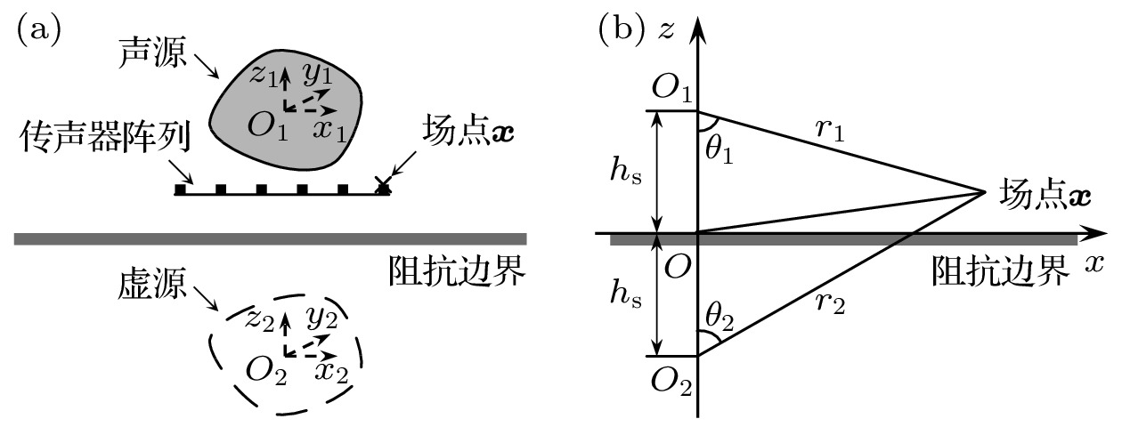
When implementing the reconstruction of the sound field radiated directly from a source located in a half-space, the half-space basis functions need to be formulated with boundary impedance as a parameter. The boundary impedance is usually obtained via in situ acoustic impedance measurement techniques. In a reconstruction method based on expansion in half-space spherical wave basis functions, a hologram surface and a single reference microphone placed in the near-field are used to collect sound pressures. The sound pressure at the reference microphone is first reconstructed and the error of the reconstructed pressure relative to the measured pressure is then calculated. The sound pressure reflection coefficient corresponding to the minimum error is chosen as the estimated value of the reflection coefficient at each of the measurement points. Thus, this method is applicable to reconstructing the directly radiated sound pressures without knowledge of the boundary impedance, without the in situ acoustic impedance measurements necessary for conventional methods. The purpose of this work is to discuss the various parameters affecting the accuracy of reconstruction. Moreover, the boundary impedance is reconstructed based on the estimation of the reflection coefficient. In this way, an acoustic impedance measurement technique implemented via the near-field acoustical holography is proposed. Taking the source to be spherical, numerical simulations are conducted to verify the proposed method of reconstructing the boundary impedance and the directly radiated sound pressures. The influences of reference microphone coordinates, the effective flow resistivity of the boundary, and the rate of decrease of porosity with depth of the boundary on the accuracy of reconstruction are quantitatively analyzed.
2022, 71 (12): 124701.
doi: 10.7498/aps.71.20220102
Abstract +
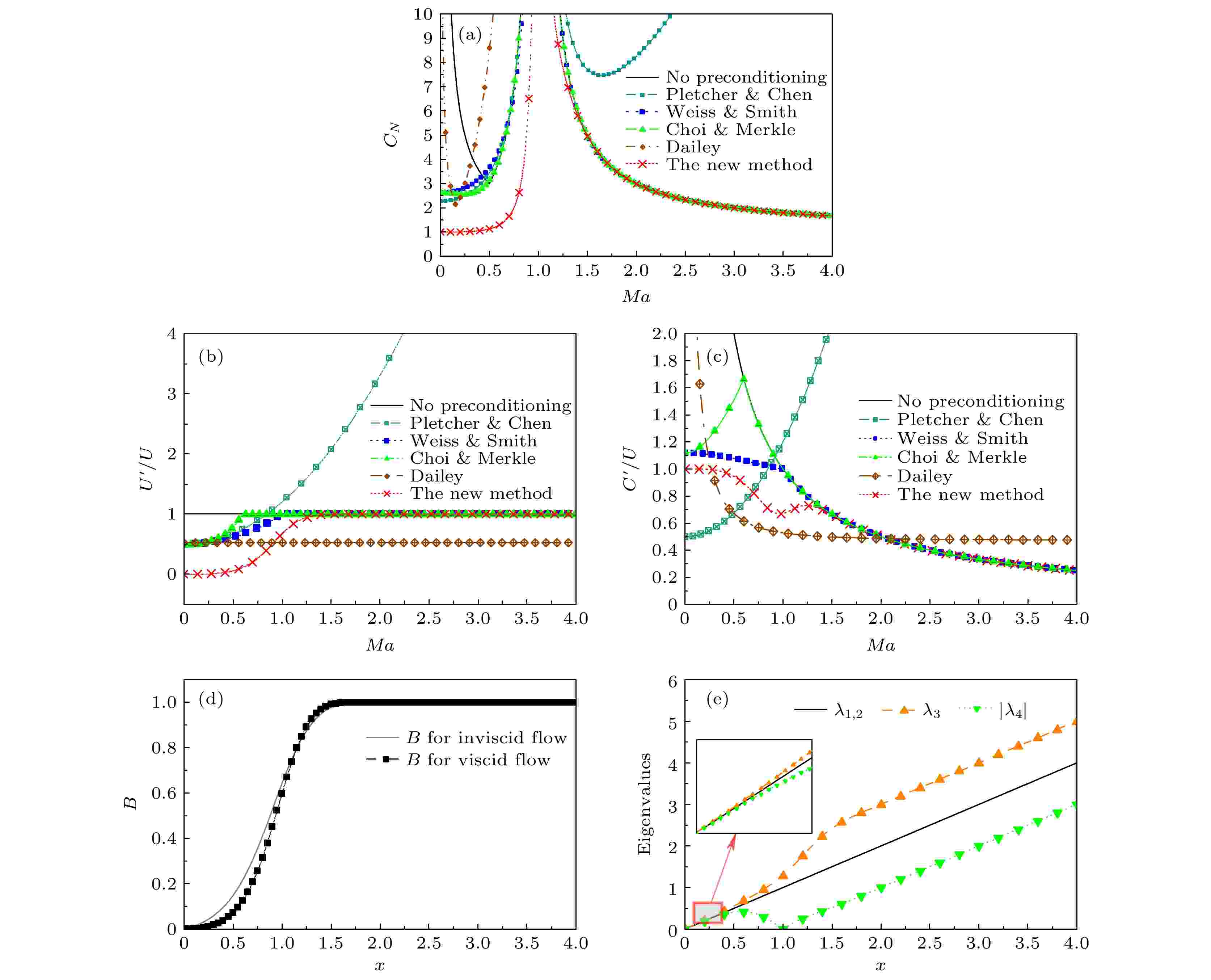
Low velocity flows often exhibit incompressible properties, and one of the most prohibitive aspects of these problems is a large number of computer resources required, including both CPU time and memory. Various numerical schemes used to calculate incompressible flow are constantly updated to accelerate convergence and reduce resource occupation, but incompressible flow is an ideal model for studying theoretical problems after all. In addition, it is a common phenomenon that high-speed and low-speed flow regions exist in the same system, and the influence of heat and volume force cannot be ignored in some cases. The artificial compressibility method is based on the idea that the numerical algorithms for compressible flows are used to solve incompressible flow. The system of compressible flow governing equations at very low Mach numbers is stiff due to the large disparity in acoustic wave speed, u + c, and the waves convecting at fluid speed, u. The preconditioning algorithm is effective to change the eigenvalues of the compressible flow equations system so as to remove the large disparity in wave speed, and the essence is to multiply the time derivatives with a suitable matrix. A function in low growth rate with Mach number as a variable is used to construct another new preconditioning matrix. Compared with other matrices of Dailey, Weiss, Choi and Pletcher, the new matrix can well improve the stiffness of the governing equations and the smoothness of eigenvalues in all-speed domain. A one-dimensional numerical example shows that the preconditioning matrix has ability to improve the efficiency of solving low-speed flow problems. These preconditioning matrices are extended to two-dimensional problems to simulate inviscid flow passing through a pipe with bulge and viscous flows passing through a flat and cavity. The results indicate that the new matrix has not only better accuracy but also higher efficiency than Weiss’s and Pletcher’s.
CONDENSED MATTER: ELECTRONIC STRUCTURE, ELECTRICAL, MAGNETIC, AND OPTICAL PROPERTIES
EDITOR'S SUGGESTION
2022, 71 (12): 127201.
doi: 10.7498/aps.71.20211962
Abstract +
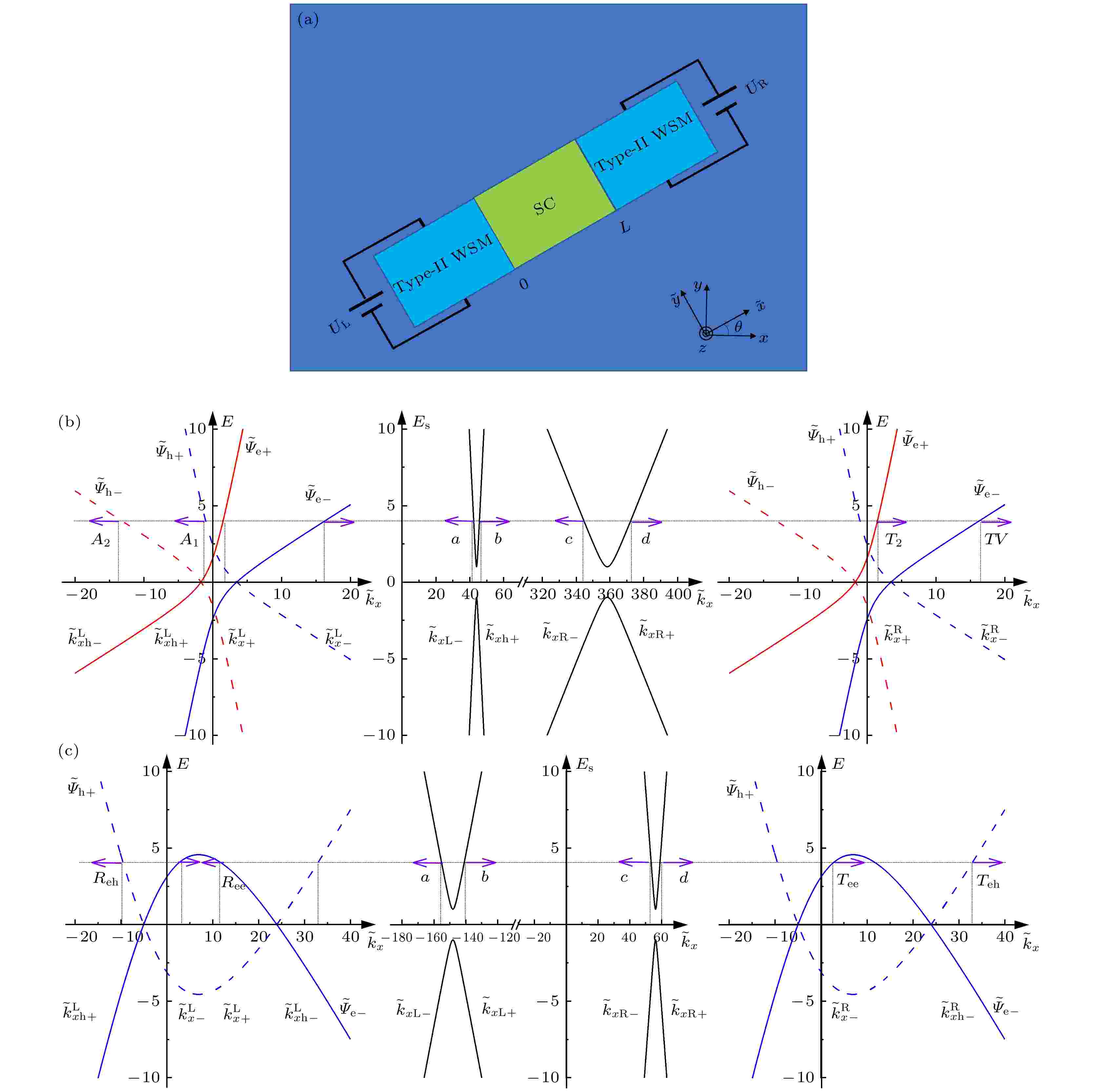
The quantum transport behavior of the normal-superconductor-normal (NSN) junction is studied theoretically based on a type-II Weyl semimetal which is rotated a certain angle. The calculation results show that the orientation angle determines the scattering mechanism of the system. In the NSN junction, there exist simultaneously two local Andreev reflections (ARs) (retro AR and specular AR) and two local election transmissions (ETs) (retro ET and specular ET) when the orientation angle is small. Moreover, the retro AR is gradually suppressed with the further increase of the orientation angle. When the orientation angle exceeds the critical angle, the scattering mechanism in NSN junction is the same as that of the NSN junction in normal mental, i.e. the normal electron reflection, normal electron transmission, retro Andreev reflection and crossed Andreev reflection take place simultaneously. In addition, the total conductance of the system is unaffected by the chemical potential, nor by the incident angle when the orientation angle is smaller than the critical angle, but decreases with the increase of the incident angle when the orientation angle is greater than the critical angle. The conductance of crossed Andreev reflection increases with incident angle increasing under some conditions.
EDITOR'S SUGGESTION
2022, 71 (12): 127301.
doi: 10.7498/aps.71.20212439
Abstract +
Spintronics is a particularly hot topic in recent years, which has aroused much attention. The spin freedom of electrons can be used to construct logic devices and memory devices. Generally, the most important spintronic properties are found in half-metal ferromagnets, which are considered as the ideal materials for building spintronic devices due to their ability to provide fully spin-polarised conduction electrons. Numerous experimental data and theoretical studies have confirmed that the intercalation, doping and adsorption of transition metal atoms can induce magnetic properties in two-dimensional WS2 material. Therefore, half-metal ferromagnets formed by doping WS2 play an important role in the field of spintronics. In this paper, we investigate the electronic structure, magnetic and optical properties of the WS2 doped with transition metal atoms X (X = Mn, Tc, Re) by the first-principles plane wave method based on density functional theory. The results show that the WS2 system doped with transition metal atoms X is more stable under S-rich condition than under W-rich condition. Especially, the WS2 system doped with Tc has a minimum value of formation energy of –1.292 eV under S-rich condition. After doping with Mn, impurity levels appear in the spin-up channels, resulting in the WS2 system changing from a non-magnetic semiconductor to half-metal ferromagnet with a magnetic moment of 1.001 $ {\text{μ}}_{\text{B}} $ . Moreover, in the Mn-doped system, the densities of states are asymmetric in the spin-up channel and the spin-down channel. After being doped with Tc and Re, the systems are transformed into non-magnetic N-type semiconductors, and the densities of states in spin-up and spin-down channels are symmetric in Tc doping system and Re doping system. Whereafter, the spin orbit splitting of the impurity states near the Fermi level EF decreases successively from Mn to Re doped WS2 systems. Compared with the undoped two-dimensional WS2, the transition metal atoms X doped WS2 systems show that all doped systems not only have a significant red shift of optical absorption edges but also enhance peak value in infrared and visible light region, implying that the transition metal atoms X doped WS2 systems have great application prospects in infrared and visible light detection. We hope that thepresent study of two-dimensional WS2 will provide useful theoretical guidance for future experiments to explore low-dimensional spintronic materials.


2022, 71 (12): 127501.
doi: 10.7498/aps.71.20220166
Abstract +
Epitaxial FeGa/IrMn bilayers with exchange biases along the FeGa[100] and [110] directions are prepared on MgO(001) single crystal substrates by magnetron sputtering through controlling the orientation of the external field in situ applied during growth. The effect of the exchange bias orientation on the magnetic switching process and the magnetic switching field are studied. The X-ray φ-scan indicates that the FeGa layer is epitaxially grown with a 45° in-plane rotation on the MgO(001) substrate along the FeGa(001)[110] direction and the MgO(001)[100] direction. The measurements of the angular dependence of the ferromagnetic resonance field and the corresponding fitting to the Kittel equation show that the samples have a superposition of fourfold symmetric magnetocrystalline anisotropy $ {K}_{1} $ , unidirectional magnetic exchange bias anisotropy $ {K}_{\mathrm{e}\mathrm{b}} $ , and uniaxial magnetic anisotropy $ {K}_{\mathrm{u}} $ with configuration of $ {K}_{\mathrm{e}\mathrm{b}}//\left[100\right] $ or $ {K}_{\mathrm{e}\mathrm{b}}//\left[110\right] $ . The combined longitudinal and transverse magneto-optical Kerr effect measurements show that sample with $ {K}_{\mathrm{e}\mathrm{b}}//\left[100\right] $ exhibits square loops, asymmetrically shaped loops, and one-sided two-step loops in different external magnetic field directions. In contrast, the sample with $ {K}_{\mathrm{e}\mathrm{b}}//\left[110\right] $ exhibits one-sided two-step and two-sided two-step loops as the magnetic field orientation changes. Because the $ {K}_{1} $ is superimposed by $ {K}_{\mathrm{u}} $ and $ {K}_{\mathrm{e}\mathrm{b}} $ , the in-plane fourfold symmetry of the magnetic anisotropy energy is broken. The local minima are no longer strictly along the in-plane $ \left\langle{100}\right\rangle $ directions, but make a deviation angle which depends on the relative orientation and strength of magnetic anisotropy. A model based on the domain wall nucleation and propagation is proposed with considering the different orientations of $ {K}_{\mathrm{e}\mathrm{b}} $ , which can nicely explain the change of the magnetic switching route with the magnetic field orientation and fit the angular dependence of the magnetic switching fields, indicating a significant change of domain wall nucleation energy as the orientation of $ {K}_{\mathrm{e}\mathrm{b}} $ changes.


2022, 71 (12): 127502.
doi: 10.7498/aps.71.20220168
Abstract +
The magnetization reversal resulting from the thermal fluctuation is irreversible for overcoming the energy barrier, ant it is called the thermally assisted tunneling. In this paper the relaxation in magnetizaition reversal resulting from the thermal fluctuation is observed in Pr-Fe-B permanent magnet. The dependence of magnetic moment on the time natural logarithm is the same as that on the energy barrier in the thermally assisted tunneling. So the relaxation in magnetization reversal originates from the macroeffect of magnons which follow Bose distribution law. The critical size in the irreversible magnetization reversal obtained by the fluctuation field is on a nanometer scale and close to the theoretical domain wall size, indicating that the thermally assisted magnetization reversal undergoes the nucleation and de-pinning of domain wall. The increase of coupling volume will reduce the possibility of magnons tunneling in magnetization reversal due to the weakening effect of thermal fluctuation. The variation of fluctuation field with the field verifies the effect of exchange coupling in Pr-Fe-B magnets, and the calculated value of fluctuation field is consistent with the aftereffect of thermal activation. With the increase of temperature the thermal fluctuation energy increases, and though the aftereffect of thermal fluctuation weakens due to the exchange coupling, the ratio of thermal fluctuation aftereffect to coercivity increases in Pr-Fe-B magnet.
INTERDISCIPLINARY PHYSICS AND RELATED AREAS OF SCIENCE AND TECHNOLOGY
2022, 71 (12): 128101.
doi: 10.7498/aps.70.20220288
Abstract +
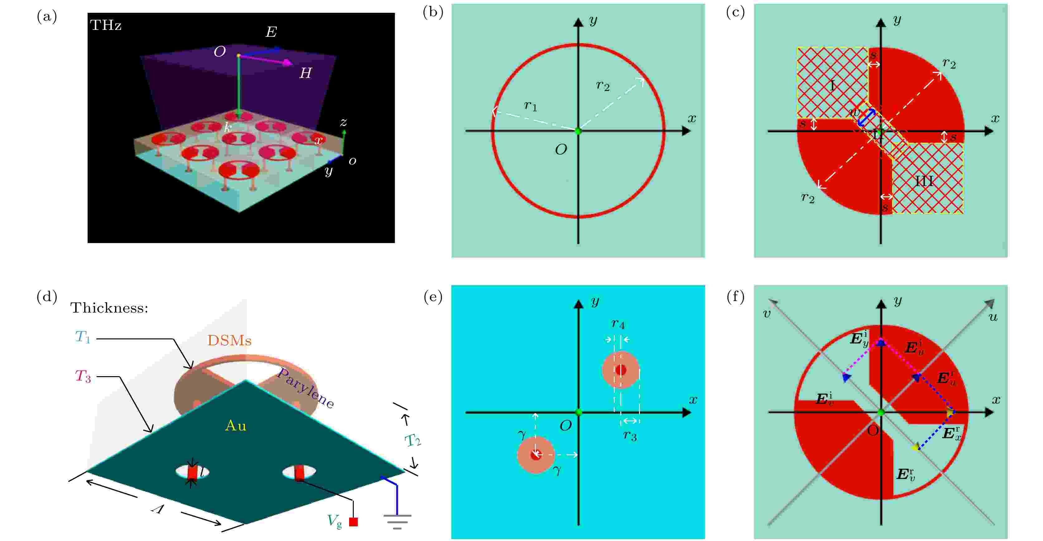
Combined with the Dirac semimetals (DSMs), which is a new type of material and also called 3D graphene, a tunable wideband terahertz polarization conversion metasurface based on an anisotropic configuration is studied, in which the DSM wire array is beneficial to the regulation of Fermi energy. The results show that the metasurface can realize wideband and highly efficient polarization conversion, and has the property of half wave plate at the resonant modes. These characteristics are derived from the excitation of localized surface plasmon resonance (LSPR) and the anisotropy of structure itself. When the incident angle changes in a range of $0^\circ $ –$40^\circ $ , the high efficiency of wideband polarization conversion can be maintained. When it is greater than $40^\circ $ , the wideband polarization conversion gradually changes into the dual-band conversion or the multi-band conversion. Furthermore, it is found that in the process of increasing the Fermi energy of AlCuFe from 65 to 140 meV, the polarization conversion ratio can be maintained at a high level, and the conversion performance changes from single-band conversion into wideband conversion, and then into wideband conversion with wider band and single-band conversion with narrower band. At the same time, by discussing the metasurface combined with the different DSM, it is concluded that the better the metallic property of DSMs, the better the wideband polarization conversion performance of the corresponding metasurface is. Finally, the numerical results are verified by the multiple interference theory based on the Fabry-Pérot-like resonance cavity.


2022, 71 (12): 128501.
doi: 10.7498/aps.71.20220172
Abstract +
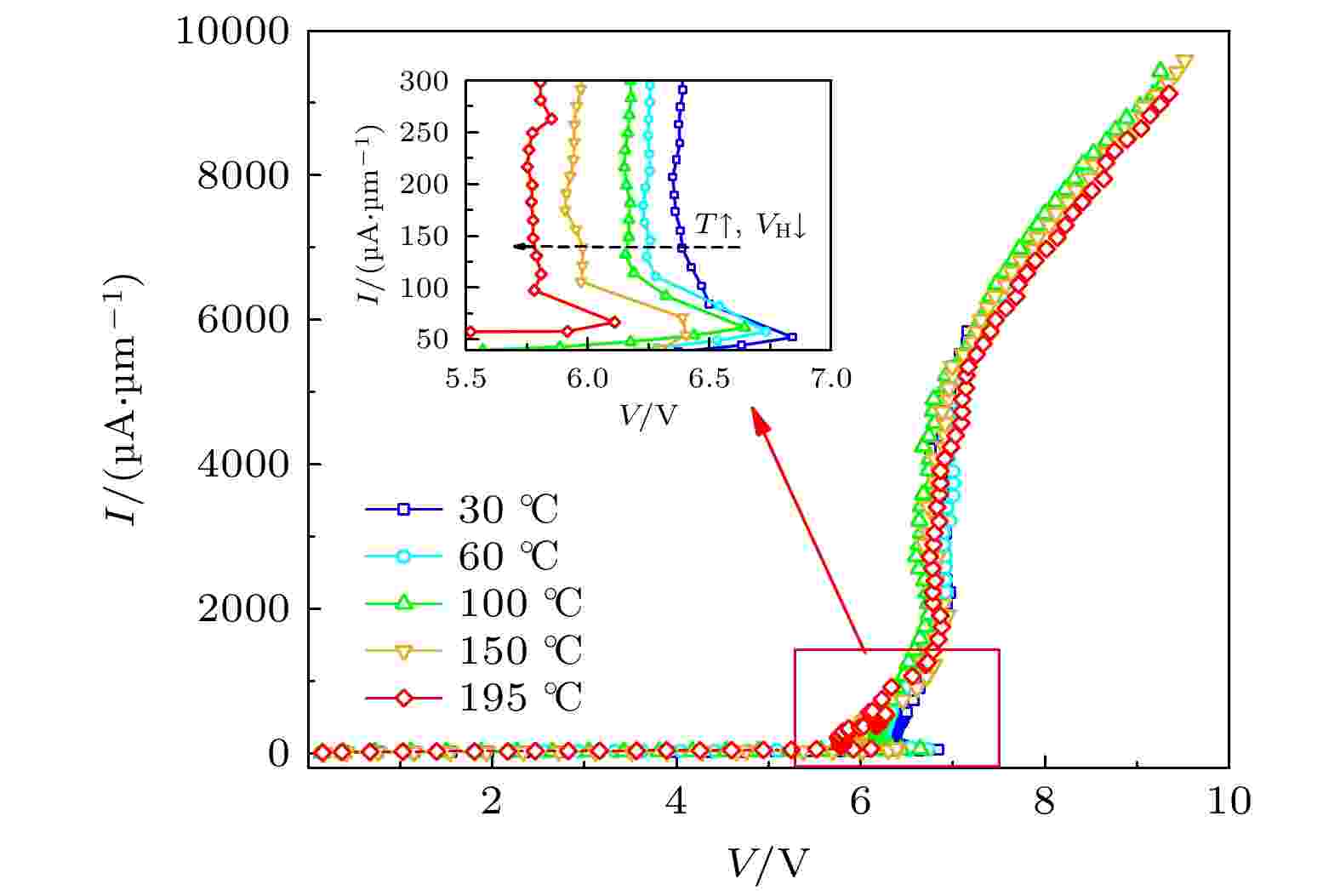
The holding voltage of electrostatic discharge (ESD) protecting structure is the critical parameter to determine the latch-up performance of the protecting device, but the thermal change of ESD device parameters lead the protecting device to suffer latch-up risk at high ambient temperature. In this paper, the holding characteristics of the ESD protecting device at various ambient temperatures ranging from 30 ℃ to 195 ℃ are studied. The investigated ESD structure is the N-channel metal oxide semiconductor (NMOS) transistors fabricated with the 0.18 μm partially depleted silicon-on-insulator process. The ESD characteristics of the device are measured by the transmission line pulse test system at different ambient temperatures. The test results show that the holding voltage (VH) decreases with temperature increasing. The TCAD simulation is carried out to support and analyze the experimental results, and the same trend of VH versus temperature is obtained. Through the analysis of simulation results and theoretical derivation, the underlying physical mechanisms related to the effects of temperature on VH and holding current (IH) are discussed in detail. When the drain is subjected to the same current pulsing and the Source and Body are both grounded, the distributions of current density, electric potential, and injected electron density of NMOS at various temperatures are extracted and analyzed. When the Drain, Source, and Body are all grounded, the distributions of the electrostatic field at various temperatures are extracted and analyzed. The distribution of electric potential in NMOS indicates that the voltage drop on the Drain-Body junction (VDB) is affected by ambient temperature significantly, and the variation of VDB dominates the variation trend of VH with temperature increasing. The reducing electrostatic field and increasing injected electron density with temperature decreasing contribute to the decreasing of VDB. The trend of IH and parasitic Body resistance (RBody) weakens the temperature dependence of the VH. The current gain of parasitic bipolar transistor (β) decreases with ambient temperature rising, which is the main contributor to the decreasing of IH. Therefore, increasing IH and RBody is helpful in reducing the temperature dependence of the latch-immune ESD protection structure.
2022, 71 (12): 128701.
doi: 10.7498/aps.71.20212091
Abstract +
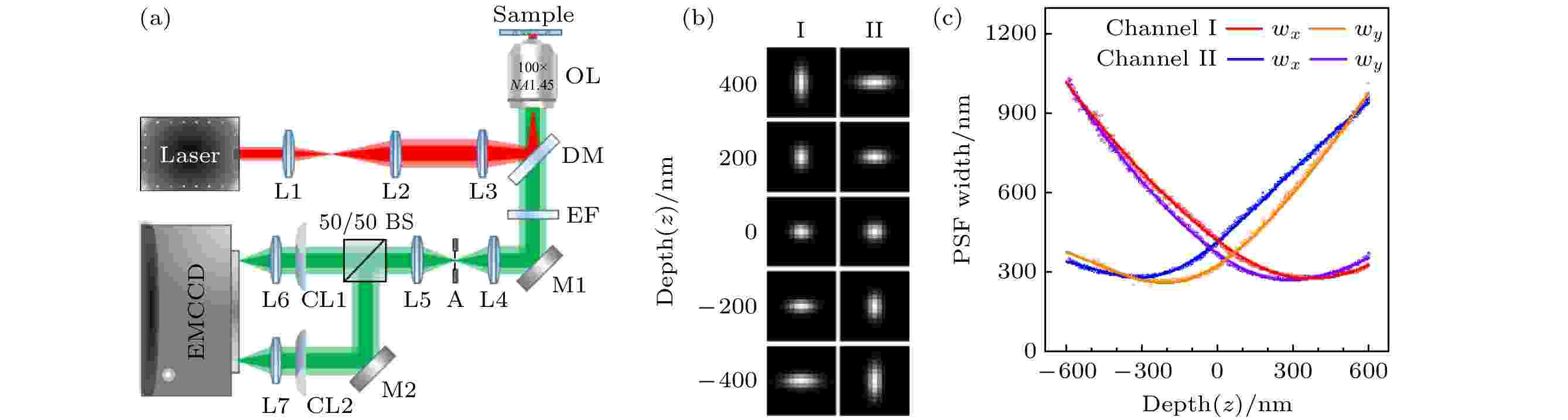
Single molecule localization microscopy (SMLM) detects and locates sparsely luminous single fluorescent molecules to achieve super-resolution imaging at nanoscale spatial resolution. In order to improve the temporal resolution, it is necessary to increase the density of the simultaneously emitting molecules. However, with the increase of the density, the point spread function (PSF) of different molecules will overlap severely on the detector, resulting in reduced spatial resolution, especially for three-dimensional (3D) SMLM. To solve this problem, a high density 3D-SMLM imaging method based on orthogonal astigmatism is proposed. Analysis and numerical simulation study for the method are carried out and presented. The main idea of the proposed orthogonal astigmatic method is to split the collected fluorescence in a SMLM microscope into two beams, each of which passes through a separate channel with a cylindrical lens and arrives at a specific region on the same detector. The two cylindrical lenses have the same optical parameters, but their orientations are set to be orthogonal to each other. They are used to obtain both positive and negative astigmatic PSF images of the same fluorescent molecule. Then, a linear projection model of the imaging process is established, and the 3D localization of the fluorescent molecules is realized by using a compression sensing algorithm. The results show that the two orthogonal cylindrical lenses produce a pair of astigmatic PSFs for one single molecule so that different PSF pairs between different molecules have lower mutual correlation, and thus the 3D localization accuracy for high density imaging can be significantly improved as compared with traditional astigmatic method, in which one single cylindrical lens is used. The larger the defocusing degree, the greater the shape difference between the two astigmatic PSFs is, and the more obvious this advantage.
