-
Localized surface plasmon (LSP) generated by nanostructure subjected to the excitation of surface plasmon polariton (SPP) possesses stronger near-field enhancement and special spectral and dynamic responses, thereby providing a new idea for exploring the interaction between light and matter. Meanwhile, this scheme can also release the signal background noise and structural thermal effect, and improve the performances of plasmonic components and sensing detectors based on LSP. However, the current research in this aspect is still insufficient. In this paper, we investigate the near-field characteristics of a plasmon composite structure composed of plasmon focusing lens and gold nanorod under the excitation of dual-beam by using finite-difference time-domain (FDTD) method. The result shows that the near-field intensity control on the upper surface and in the gap position of the nanorod can be achieved by adjusting the relative time delay between the first light beam (used to excite SPP) and the second light beam (used to excite LSP). Specifically, the maximum adjustment range of the near-field intensity corresponding to 770 nm resonant mode in the gap position is about 23, and the adjustment period is about 2.4 fs. In a resonant mode dominated by SPP at a wavelength of 999 nm, the adjustment range of near-field intensity is as small as 6, and the adjustment period is about 4 fs. On the upper surface of the structure, the adjustment range of the near-field intensities of the two resonant modes (719 nm and 802 nm) are basically the same (about 15), and their adjustment periods are 2.4 fs and 2.8 fs. The achievement of the near field control is attributed to the coherent superposition of SPP-excited LSP with light-excited LSP. In addition, the dephasing time of the coupling field is investigated by using a quasi- normal mode. It is found that the nanorod structure will correspond to different dephasing time under different relative time delay between two excitation light beams. Specifically, for the time delay of 0.72 fs (Δt = 0.72 fs), the corresponding dephasing times for both modes are the same (6.0 fs). For Δt = 1.92 fs, the dephasing time of the longer-wavelength mode is 7.1 fs, and the one of the shorter-wavelength mode is 5.8 fs. We attribute the difference in dephasing time to different coupling strengths between the two modes at different delay times. This study may further promote the application of plasmons in the fields of surface-enhanced Raman scattering and plasmon assisted catalysis.
-
Keywords:
- plasmonics /
- surface plasmon polariton interacts with localized surface plasmon /
- near-field control /
- finite-difference time-domain
[1] Barnes W L, Dereux A, Ebbesen T W 2003 Nature 6950 824
[2] Jin X, Xue L, Xiong J C, Ye S W, et al. 2023 In Plasmonics in Biology and Medicine XX, SPIE 12396 34
 Google Scholar
[3] Ren Y, Li T, Zhou J, et al. 2023 Opt. Mater. Express 3 796
 Google Scholar
[4] Wu N, Zhang Y, Ma H, et al. 2021 Prog. Electromagn. Res. 172 23
 Google Scholar
[5] Ahmed A, Gordon R 2011 Nano Lett. 4 1800
 Google Scholar
[6] Cui W, Peng W, Yu L, et al. 2019 Nanomaterials 3 334
 Google Scholar
[7] Liu L, Li Z 2022 Prog. Electromagn. Res. 173 93
 Google Scholar
[8] Fainman Y, Tetz K, Rokitski R, Pang L I N 2006 Opt. Photonics News 17 24
 Google Scholar
[9] Ritchie R H 1957 Phys. Rev. 106 874
 Google Scholar
[10] Zhou Y C, Zhang X C, Hu X, Tang L L, Cao Y, Li J Q, Wang J, Dong Z G 2021 J. Appl. Phys. 8 083103
 Google Scholar
[11] Zeng P, Cadusch J, Chakraborty D, Smith T A, Roberts A, Sader J E, Davis J, Gómez D E 2016 Nano Lett. 16 2651
 Google Scholar
[12] Lerman G M, Yanai A, Levy U 2009 Nano Lett. 9 2139
 Google Scholar
[13] Liu Z, Steele J M, Lee H, Zhang X 2006 Appl. Phys. Lett. 88 171108
 Google Scholar
[14] Liu Z, Steele J M, Srituravanich W, Pikus, Y, Sun C, Zhang X 2005 Nano Lett. 5 1726
 Google Scholar
[15] Darak M S, Mote R G, Shukla S 2018 Ann. Phys. 530 1800193
 Google Scholar
[16] Qin Y, Ji B, Song X, Lin J 2021 JOSA B 38 C58
 Google Scholar
[17] Lerman G M, Yanai A, Ben-Yosef N, Levy U 2010 Opt. Express 18 10871
 Google Scholar
[18] Chen W, Abeysinghe D C, Nelson R L, Zhan Q. 2009 Nano Lett. 9 4320
 Google Scholar
[19] Rahbany N, Geng W, Montiel R S, Cruz S D L, Méndez E R, Blaize S, Couteau R B C 2016 Plasmonics 11 175
 Google Scholar
[20] Podbiel D, Kahl P, Makris A, et al. 2017 Nano Lett. 17 6569
 Google Scholar
[21] Yang S, Chen W, Nelson R L, Zhan Q 2009 Opt. Lett. 34 3047
 Google Scholar
[22] Chen W, Abeysinghe D C, Nelson R L, Zhan Q 2010 Nano Lett. 10 2075
 Google Scholar
[23] Fang Z, Peng Q, Song W, et al. 2011 Nano Lett. 11 893
 Google Scholar
[24] Müller M, Kravtsov V, Paarmann A, Raschke M B, Ernstorfer R 2016 ACS Photonics 3 611
 Google Scholar
[25] Ciappina M F, Pérez-Hernández J A, Landsman A S, et al.M. 2017 Rep. Prog. Phys. 80 054401
 Google Scholar
[26] Fang N, Lee H, Sun C, Zhang X 2005 Science 308 534
 Google Scholar
[27] Willets K A, Wilson A J, Sundaresan V, Joshi P B 2017 Chem. Rev. 117 7538
 Google Scholar
[28] Srituravanich W, Pan L, Wang Y, Sun C, Bogy D B, Zhang X 2008 Nat. Nanotechnol. 3 733
 Google Scholar
[29] Xia M, Zhang P, Qiao K, Bai Y, Xie Y H 2016 J. Phys. Chem. C 120 527
 Google Scholar
[30] Knight M W, Sobhani H, Nordlander P, Halas N J 2011 Science 332 702
 Google Scholar
[31] Zijlstra P, Paulo P, Orrit M 2012 Nat. Nanotechnol. 6 737
 Google Scholar
[32] Kauranen M, Zayats A V 2012 Nat. Photonics 6 737
 Google Scholar
[33] Seok T J, Jamshidi A, Kim M, et al. 2011 Nano Lett. 11 2606
 Google Scholar
[34] Fernandez-Garcia R, Rahmani M, Hong M, Maier S A, Sonnefraud Y 2013 Opt. Express 21 12552
 Google Scholar
[35] Chu Y, Zhu W, Wang D, Crozier K B 2011 Opt. Express 19 20054
 Google Scholar
[36] Wang D, Zhu W, MD Best, Camden J P, Crozier K B 2013 Nano Lett. 13 2194
 Google Scholar
[37] Sun B, Ji B, Lang P, Qin Y, Lin J 2022 Opt. Commun. 505 127498
 Google Scholar
[38] Zhe S Lei S, Yao C 2016 Opt. Express 24 16052
 Google Scholar
[39] Lalanne P, Hugonin J P, Liu H. T, Wang B 2009 Surf. Sci. Rep. 64 453
 Google Scholar
[40] Johnson P B, Christy R W 1972 Phys. Rev. B 6 4370
 Google Scholar
[41] Chu Y, Crozier K B 2009 Opt. Lett. 34 244
 Google Scholar
[42] Farhang A, Bigler, Martin O J 2013 Opt. Lett. 38 4758
 Google Scholar
[43] Schertz F, Schmelzeisen M, Mohammadi R, Kreiter M, Elmers H J, Sch Nhense G 2012 Nano Lett. 2 1885
 Google Scholar
[44] Ma Y, Huang Y, Zhu Y, et al. 2023 Nanomaterials 13 492
 Google Scholar
[45] Shen Q, Boyce A M, Yang G, Mikkelsen M H 2019 ACS Photonics 6 1916
 Google Scholar
[46] Wang L M, Petek H 2013 Laser Photonics Rev 7 1003
 Google Scholar
[47] Wang Y, Ming C, Zhang Y, Xu J, Feng F, Li L, Yuan X 2020 Opt. Express 28 33516
 Google Scholar
[48] Rahbany N, Geng W, Bachelot R, Couteau C 2018 Nanotechnology 28 185201
 Google Scholar
[49] 冯仕靓, 王靖宇, 陈舒, 孟令雁, 沈少鑫, 杨志林 2019 物理学报 68 147801
 Google Scholar
Feng S L, Wang J Y, Chen S, Meng L Y, Shen S X, Yang Z L 2019 Acta Phys. Sin. 68 147801
 Google Scholar
[50] Zhang Q, Li G C, Lo T W, Lei D Y 2018 J. Opt. 20 024010
 Google Scholar
[51] Lemke C, Lei Ner T, Evlyukhin A, et al. 2014 Nano Lett. 5 2431
 Google Scholar
[52] Mårsell E, Losquin A, Svärd R, et al. 2015 Nano Lett. 15 6601
 Google Scholar
[53] Ji B, Qin J, Tao H, Hao Z, Lin J 2016 New J. Phys. 18 093046
 Google Scholar
[54] Melchior P, Bayer D, Schneider C, Fischer A, Rohmer M, Pfeiffer W, Aeschlimann M 2011 Phys. Rev. B 83 235407
 Google Scholar
[55] Hensen M, Huber B, Friedrich D, et al. 2019 Nano Lett. 19 4651
 Google Scholar
[56] Hanke T, Cesar J, Knittel V, Trügler A, Hohenester U, Leitenstorfer A, Bratschitsch R 2012 Nano Lett. 12 992
 Google Scholar
[57] Ueno K, Yang J, Sun Q, et al. 2019 Appl. Mater. 14 159
 Google Scholar
[58] Yang J H, Sun Q, Ueno K, et al. 2018 Nat. Commun. 9 4858
 Google Scholar
-
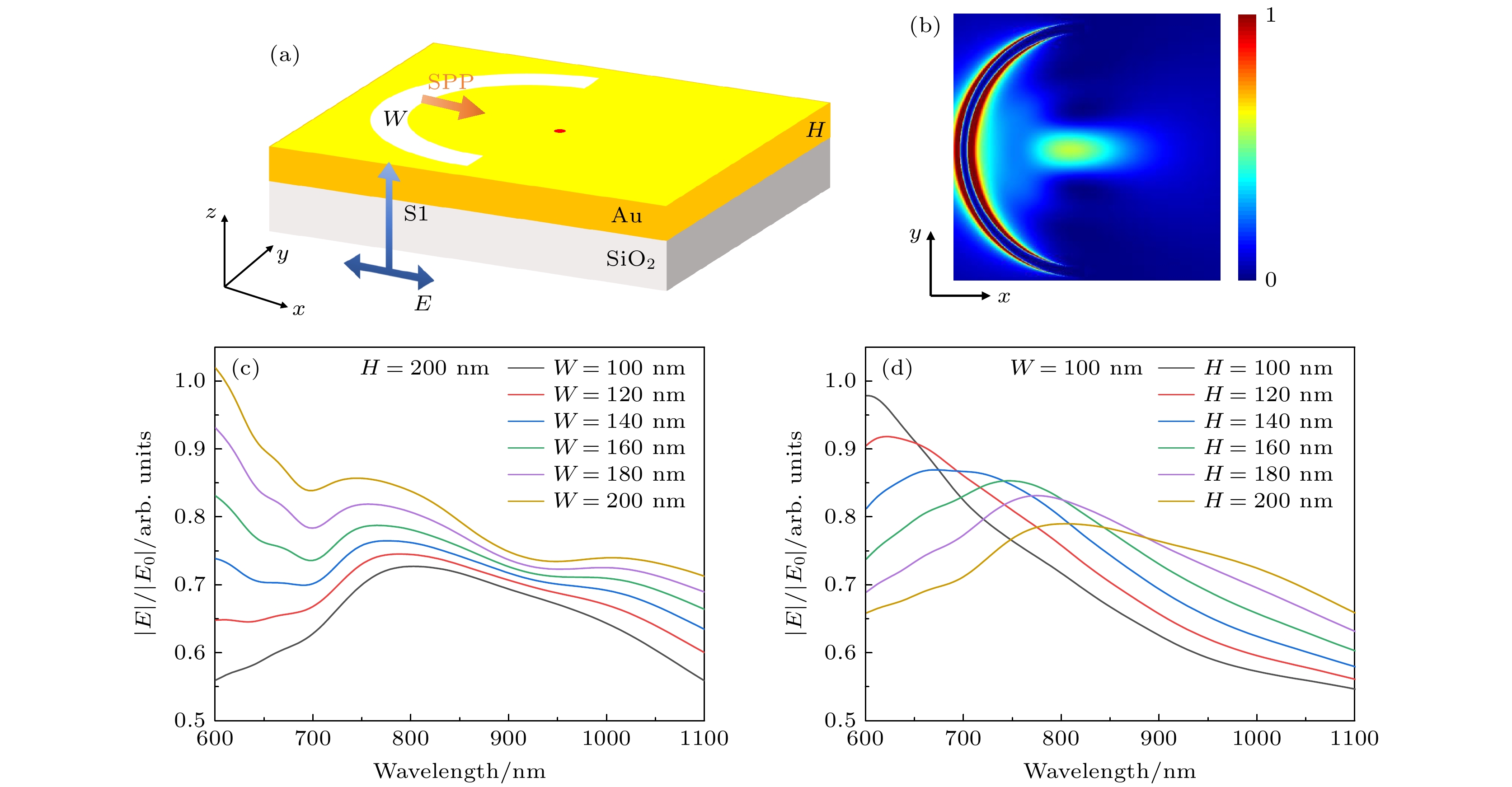
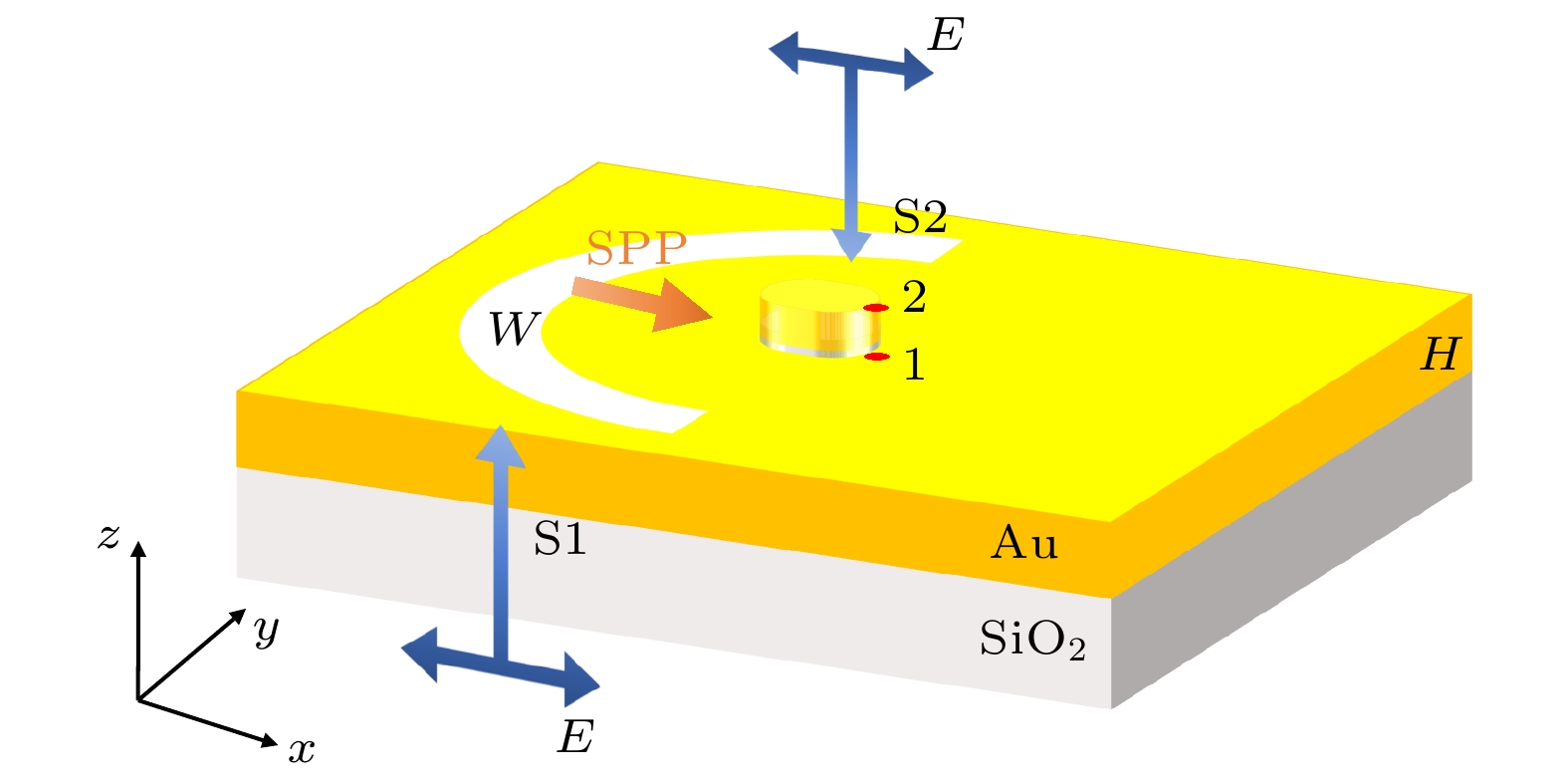
图 2 表面等离激元聚焦透镜结构参数对聚焦焦斑强度的影响 (a)表面等离激元聚焦透镜结构示意图; (b)表面等离激元透镜近场分布图像; (c)狭缝宽度W对聚焦焦斑处近场强度的影响; (d)狭缝厚度H对聚焦焦斑处近场强度的影响
Figure 2. Effect of structural parameters of surface plasmon focusing lens on focal spot intensity: (a) Schematic diagram of the surface plasmon focusing lens; (b) near-field distribution of the surface plasmon lenses; (c) effect of slit width W on near-field strength at focal spot; (d) effect of slit thickness H on near-field strength at focal spot.
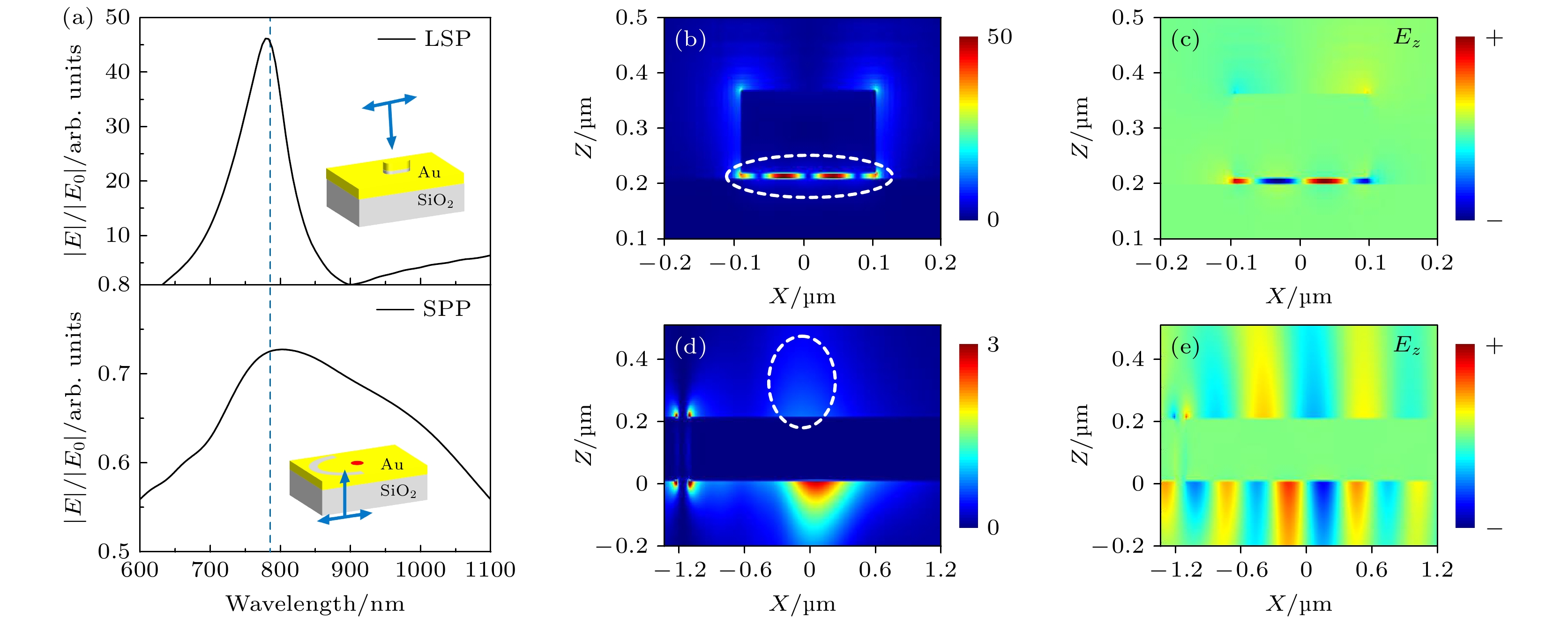
图 3 表面等离激元透镜与金纳米棒光学响应 (a)金纳米棒结构(上图)与等离激元聚焦透镜结构(下图)近场强度分布曲线; 波长在800 nm金纳米棒近场强度x-z平面分布图(b)和Ez分布图(c); 波长在800 nm附近表面等离激元透镜近场强度x-z平面分布图(d)和Ez分布图(e)
Figure 3. Optical response of the surface plasmon focusing lens and the gold nanorod: (a) Near-field intensity spectra of gold nanorod structure (top) and plasmon focusing lens structure (bottom); near-field intensity distribution (b) and Ez component distribution (c) of gold nanorods at the wavelengths of 800 nm; near-field intensity distribution (d) and Ez component distribution (e) of the surface plasmon focusing lens at the wavelengths of 800 nm
图 4 间隙位置近场强度光谱曲线以及共振波长处近场强度调控曲线 (a)间隙位置近场强度光谱曲线, 黑色曲线为相对时间延时Δt = 0.72 fs时, SPP&S2-nanorod激发条件, 红色曲线和蓝色曲线分别代表S2-nanorod 和SPP-nanorod激发条件; (b)共振波长770 nm (黑色曲线)和共振波长999 nm (红色曲线)处, 不同双光束相对时间延时对应的近场强度
Figure 4. Near-field intensity spectrum at gap position and near-field intensity regulation related with relative time delay between two laser pulses at resonant wavelength: (a) Near-field intensity spectrum for gap positions, the black curve corresponds to SPP&S2-nanorod at the relative time delay Δt = 0.72 fs; the red and blue curve corresponds to S2-nanorod and SPP-nanorod, respectively; (b) relative time delay dependent near field intensity at the resonance wavelength of 770 nm (black curve) and 999 nm (red curve), respectively.
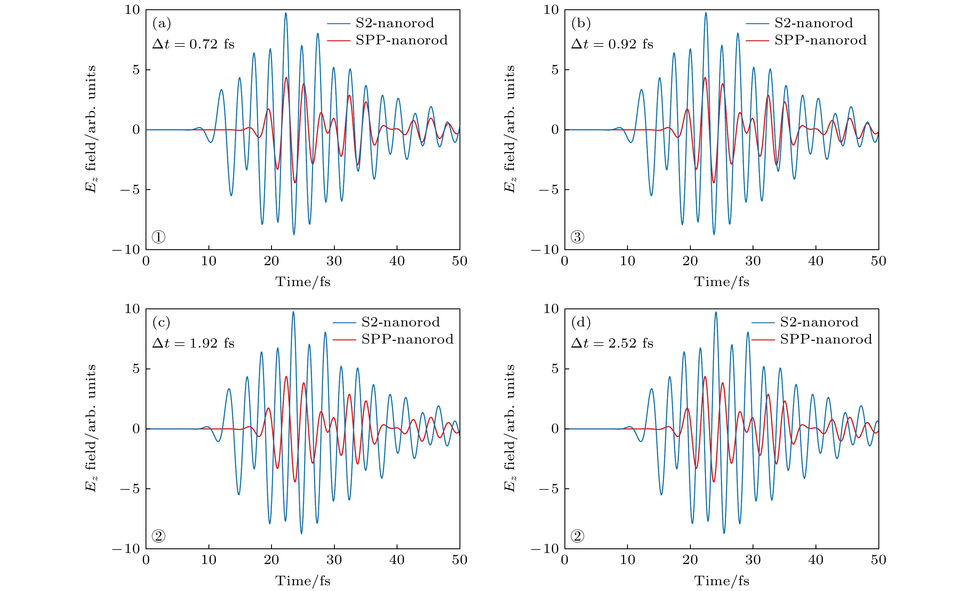
图 5 间隙位置Ez分量动力学演化曲线 (a)—(d)对应于图4(b)中①③②④位置. 蓝色曲线为S2-nanorod; 红色曲线表示SPP-nanorod条件下, 图中蓝色线的起始时间根据相对延迟数进行了调整
Figure 5. Dynamics evolution of Ez component at the gap position: (a)–(d) Corresponding to the position ①③②④ in Figure 4(b), respectively. The blue and red curves correspond to S2-nanorod and SPP-nanorod, respectively. The initial time of the blue curve in the graph is adjusted based on the relative time delays.
图 6 结构上表面近场强度光谱曲线以及共振波长处近场强度调控曲线 (a)上表面近场强度分布曲线; (b)共振波长719 nm(黑色曲线)和共振波长802 nm(红色曲线)处, 不同双光束相对时间延时对应的近场强度
Figure 6. Near-field intensity spectrum at the upper surface of nanorod and near-field intensity regulation related with relative time delay between two laser pulses at resonant wavelength: (a) Near-field intensity spectrum at the upper surface of nanorod; (b) relative time delay dependent near field intensity at the resonance wavelength of 719 nm (black curve) and 802 nm (red curve), respectively.
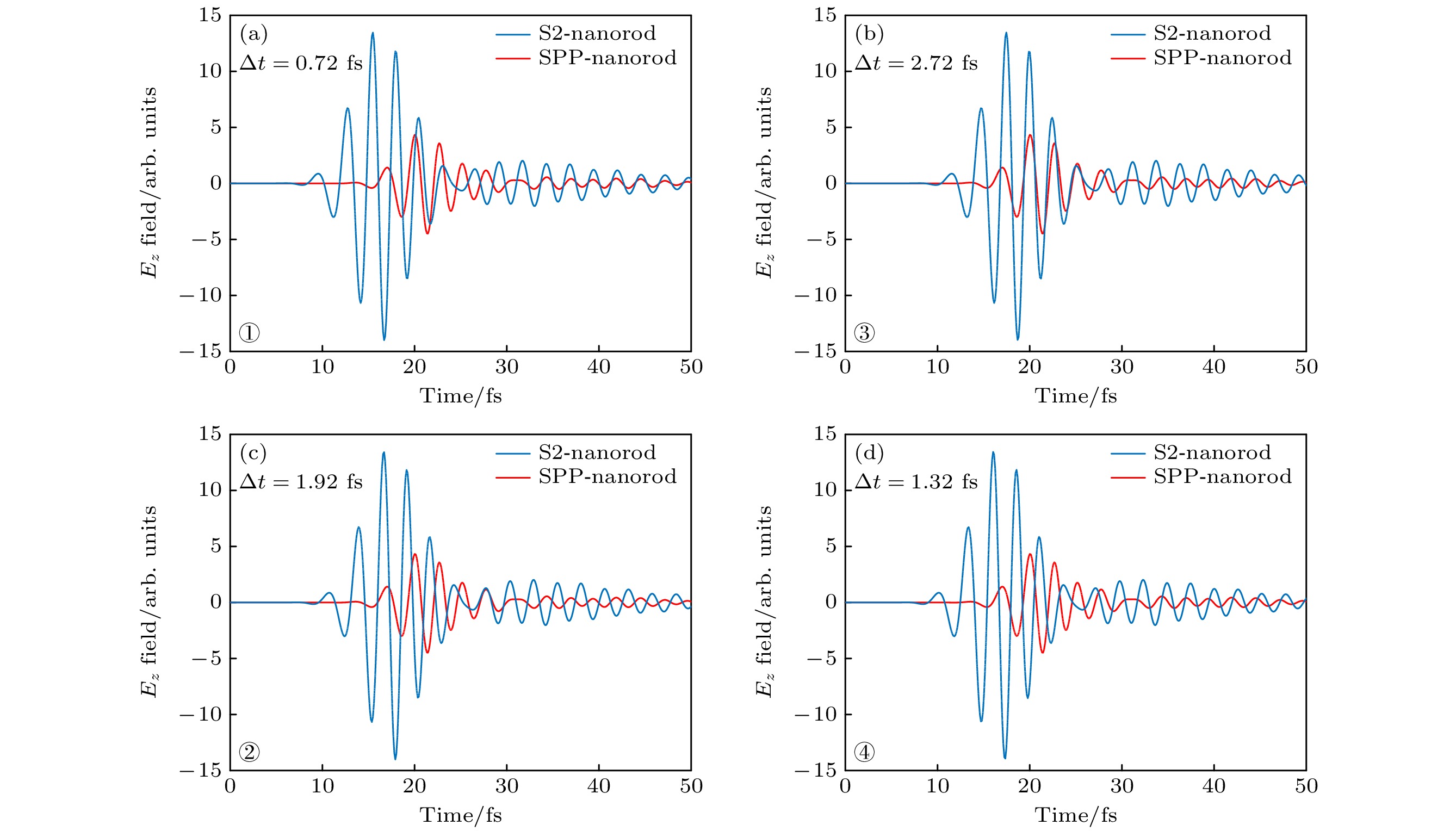
图 7 纳米棒上表面Ez分量动力学演化曲线 (a)—(d)对应于图6(b)中①③②④ 位置, 图中蓝色线的起始时间根据相对延迟数进行了调整
Figure 7. Dynamics evolution of Ez component at the upper surface of nanorod: (a)–(d) Corresponding to the position ①③②④ in Fig. 6(b), respectively. The initial time of the blue curve in the graph is adjusted based on the relative time delays.
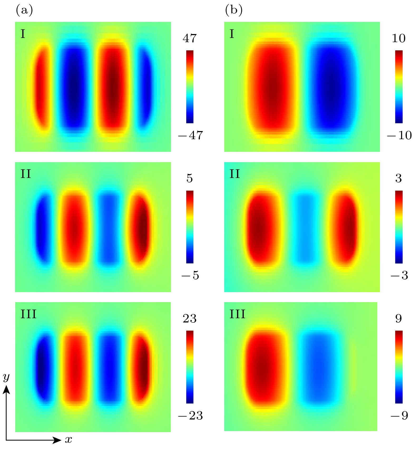
图 8 间隙位置电场强度Ez分量分布图 (a)共振波长为770 nm; (b)共振波长为999 nm. Ⅰ为S2-nanorod; Ⅱ为SPP-nanorod; Ⅲ为 SPP&S2-nanorod
Figure 8. Ez component distribution in the gap position of the nanorod: (a) The resonance wavelength is 770 nm; (b) the resonance wavelength is 999 nm. The excitation conditions corresponding to Ⅰ, Ⅱ, and Ⅲ are S2-nanorod, SPP-nanorod and SPP&S2-nanorod, respectively.
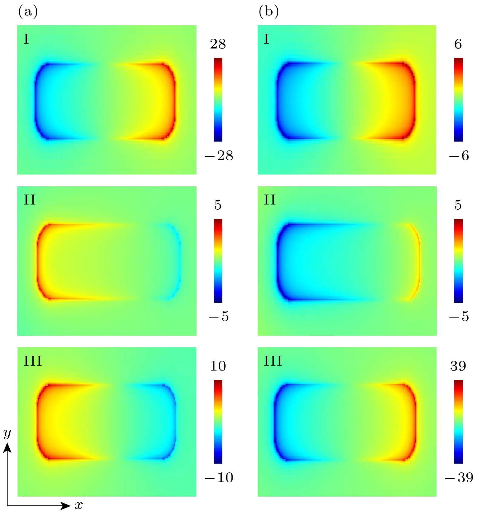
图 9 金纳米棒上表面电场强度Ez分量分布图 (a)共振波长为719 nm; (b)共振波长为802 nm. Ⅰ为S2-nanorod; Ⅱ为SPP-nanorod; Ⅲ为 SPP&S2-nanorod
Figure 9. Ez component distribution of the near field in the upper surface of the nanorod: (a) The resonance wavelength is 719 nm; (b) the resonance wavelength is 802 nm. The excitation conditions corresponding to Ⅰ, Ⅱ, and Ⅲ are S2-nanorod, SPP-nanorod and SPP&S2-nanorod, respectively.
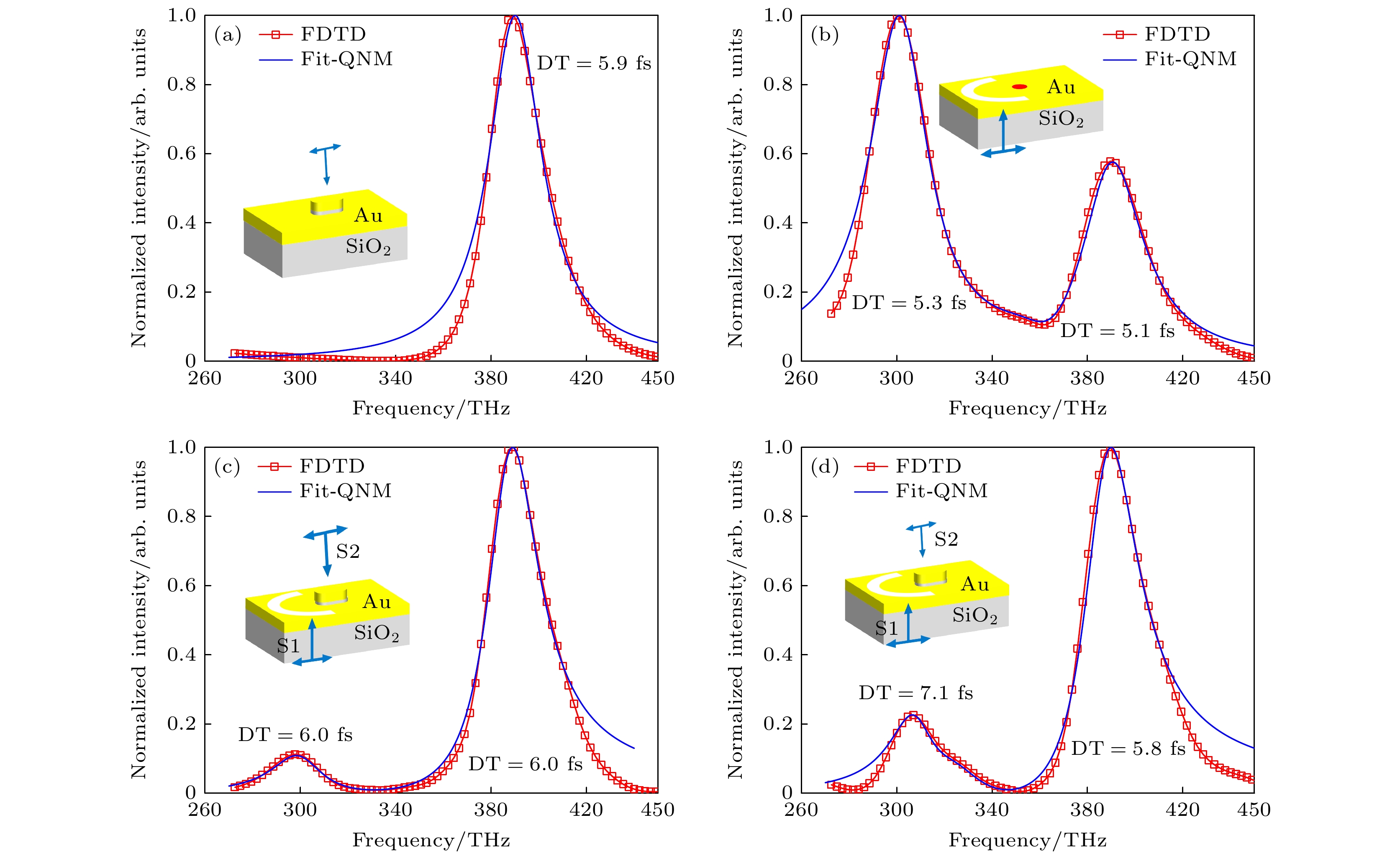
表 1 不同激发方式下LSP去相位时间和近场强度比较
Table 1. Comparison of dephasing time and near-field intensity of LSP under different excitation conditions.
S2-LSP SPP-LSP 双光束Δt = 0.72 fs 双光束Δt = 1.92 fs 波长/nm 769 996.4 769.2 1000 774.2 972.4 774.2 频率/THz 390 302 390 300 387.5 308.5 387.5 去相位时间/fs 5.9 5.3 5.1 6.0 6.0 7.1 5.8 电场强度 37.6 12. 7 9.6 15.9 48.1 13.6 28.7 -
[1] Barnes W L, Dereux A, Ebbesen T W 2003 Nature 6950 824
[2] Jin X, Xue L, Xiong J C, Ye S W, et al. 2023 In Plasmonics in Biology and Medicine XX, SPIE 12396 34
 Google Scholar
[3] Ren Y, Li T, Zhou J, et al. 2023 Opt. Mater. Express 3 796
 Google Scholar
[4] Wu N, Zhang Y, Ma H, et al. 2021 Prog. Electromagn. Res. 172 23
 Google Scholar
[5] Ahmed A, Gordon R 2011 Nano Lett. 4 1800
 Google Scholar
[6] Cui W, Peng W, Yu L, et al. 2019 Nanomaterials 3 334
 Google Scholar
[7] Liu L, Li Z 2022 Prog. Electromagn. Res. 173 93
 Google Scholar
[8] Fainman Y, Tetz K, Rokitski R, Pang L I N 2006 Opt. Photonics News 17 24
 Google Scholar
[9] Ritchie R H 1957 Phys. Rev. 106 874
 Google Scholar
[10] Zhou Y C, Zhang X C, Hu X, Tang L L, Cao Y, Li J Q, Wang J, Dong Z G 2021 J. Appl. Phys. 8 083103
 Google Scholar
[11] Zeng P, Cadusch J, Chakraborty D, Smith T A, Roberts A, Sader J E, Davis J, Gómez D E 2016 Nano Lett. 16 2651
 Google Scholar
[12] Lerman G M, Yanai A, Levy U 2009 Nano Lett. 9 2139
 Google Scholar
[13] Liu Z, Steele J M, Lee H, Zhang X 2006 Appl. Phys. Lett. 88 171108
 Google Scholar
[14] Liu Z, Steele J M, Srituravanich W, Pikus, Y, Sun C, Zhang X 2005 Nano Lett. 5 1726
 Google Scholar
[15] Darak M S, Mote R G, Shukla S 2018 Ann. Phys. 530 1800193
 Google Scholar
[16] Qin Y, Ji B, Song X, Lin J 2021 JOSA B 38 C58
 Google Scholar
[17] Lerman G M, Yanai A, Ben-Yosef N, Levy U 2010 Opt. Express 18 10871
 Google Scholar
[18] Chen W, Abeysinghe D C, Nelson R L, Zhan Q. 2009 Nano Lett. 9 4320
 Google Scholar
[19] Rahbany N, Geng W, Montiel R S, Cruz S D L, Méndez E R, Blaize S, Couteau R B C 2016 Plasmonics 11 175
 Google Scholar
[20] Podbiel D, Kahl P, Makris A, et al. 2017 Nano Lett. 17 6569
 Google Scholar
[21] Yang S, Chen W, Nelson R L, Zhan Q 2009 Opt. Lett. 34 3047
 Google Scholar
[22] Chen W, Abeysinghe D C, Nelson R L, Zhan Q 2010 Nano Lett. 10 2075
 Google Scholar
[23] Fang Z, Peng Q, Song W, et al. 2011 Nano Lett. 11 893
 Google Scholar
[24] Müller M, Kravtsov V, Paarmann A, Raschke M B, Ernstorfer R 2016 ACS Photonics 3 611
 Google Scholar
[25] Ciappina M F, Pérez-Hernández J A, Landsman A S, et al.M. 2017 Rep. Prog. Phys. 80 054401
 Google Scholar
[26] Fang N, Lee H, Sun C, Zhang X 2005 Science 308 534
 Google Scholar
[27] Willets K A, Wilson A J, Sundaresan V, Joshi P B 2017 Chem. Rev. 117 7538
 Google Scholar
[28] Srituravanich W, Pan L, Wang Y, Sun C, Bogy D B, Zhang X 2008 Nat. Nanotechnol. 3 733
 Google Scholar
[29] Xia M, Zhang P, Qiao K, Bai Y, Xie Y H 2016 J. Phys. Chem. C 120 527
 Google Scholar
[30] Knight M W, Sobhani H, Nordlander P, Halas N J 2011 Science 332 702
 Google Scholar
[31] Zijlstra P, Paulo P, Orrit M 2012 Nat. Nanotechnol. 6 737
 Google Scholar
[32] Kauranen M, Zayats A V 2012 Nat. Photonics 6 737
 Google Scholar
[33] Seok T J, Jamshidi A, Kim M, et al. 2011 Nano Lett. 11 2606
 Google Scholar
[34] Fernandez-Garcia R, Rahmani M, Hong M, Maier S A, Sonnefraud Y 2013 Opt. Express 21 12552
 Google Scholar
[35] Chu Y, Zhu W, Wang D, Crozier K B 2011 Opt. Express 19 20054
 Google Scholar
[36] Wang D, Zhu W, MD Best, Camden J P, Crozier K B 2013 Nano Lett. 13 2194
 Google Scholar
[37] Sun B, Ji B, Lang P, Qin Y, Lin J 2022 Opt. Commun. 505 127498
 Google Scholar
[38] Zhe S Lei S, Yao C 2016 Opt. Express 24 16052
 Google Scholar
[39] Lalanne P, Hugonin J P, Liu H. T, Wang B 2009 Surf. Sci. Rep. 64 453
 Google Scholar
[40] Johnson P B, Christy R W 1972 Phys. Rev. B 6 4370
 Google Scholar
[41] Chu Y, Crozier K B 2009 Opt. Lett. 34 244
 Google Scholar
[42] Farhang A, Bigler, Martin O J 2013 Opt. Lett. 38 4758
 Google Scholar
[43] Schertz F, Schmelzeisen M, Mohammadi R, Kreiter M, Elmers H J, Sch Nhense G 2012 Nano Lett. 2 1885
 Google Scholar
[44] Ma Y, Huang Y, Zhu Y, et al. 2023 Nanomaterials 13 492
 Google Scholar
[45] Shen Q, Boyce A M, Yang G, Mikkelsen M H 2019 ACS Photonics 6 1916
 Google Scholar
[46] Wang L M, Petek H 2013 Laser Photonics Rev 7 1003
 Google Scholar
[47] Wang Y, Ming C, Zhang Y, Xu J, Feng F, Li L, Yuan X 2020 Opt. Express 28 33516
 Google Scholar
[48] Rahbany N, Geng W, Bachelot R, Couteau C 2018 Nanotechnology 28 185201
 Google Scholar
[49] 冯仕靓, 王靖宇, 陈舒, 孟令雁, 沈少鑫, 杨志林 2019 物理学报 68 147801
 Google Scholar
Feng S L, Wang J Y, Chen S, Meng L Y, Shen S X, Yang Z L 2019 Acta Phys. Sin. 68 147801
 Google Scholar
[50] Zhang Q, Li G C, Lo T W, Lei D Y 2018 J. Opt. 20 024010
 Google Scholar
[51] Lemke C, Lei Ner T, Evlyukhin A, et al. 2014 Nano Lett. 5 2431
 Google Scholar
[52] Mårsell E, Losquin A, Svärd R, et al. 2015 Nano Lett. 15 6601
 Google Scholar
[53] Ji B, Qin J, Tao H, Hao Z, Lin J 2016 New J. Phys. 18 093046
 Google Scholar
[54] Melchior P, Bayer D, Schneider C, Fischer A, Rohmer M, Pfeiffer W, Aeschlimann M 2011 Phys. Rev. B 83 235407
 Google Scholar
[55] Hensen M, Huber B, Friedrich D, et al. 2019 Nano Lett. 19 4651
 Google Scholar
[56] Hanke T, Cesar J, Knittel V, Trügler A, Hohenester U, Leitenstorfer A, Bratschitsch R 2012 Nano Lett. 12 992
 Google Scholar
[57] Ueno K, Yang J, Sun Q, et al. 2019 Appl. Mater. 14 159
 Google Scholar
[58] Yang J H, Sun Q, Ueno K, et al. 2018 Nat. Commun. 9 4858
 Google Scholar
Catalog
Metrics
- Abstract views: 6974
- PDF Downloads: 179
- Cited By: 0


 DownLoad:
