Vol. 72, No. 17 (2023)
2023-09-05
SPECIAL TOPIC — Quantum transport in topological materials and devices • COVER ARTICLE
COVER ARTICLE
SPECIAL TOPIC — Quantum transport in topological materials and devices
2023, 72 (17): 177101.
doi: 10.7498/aps.72.20230634
Abstract +
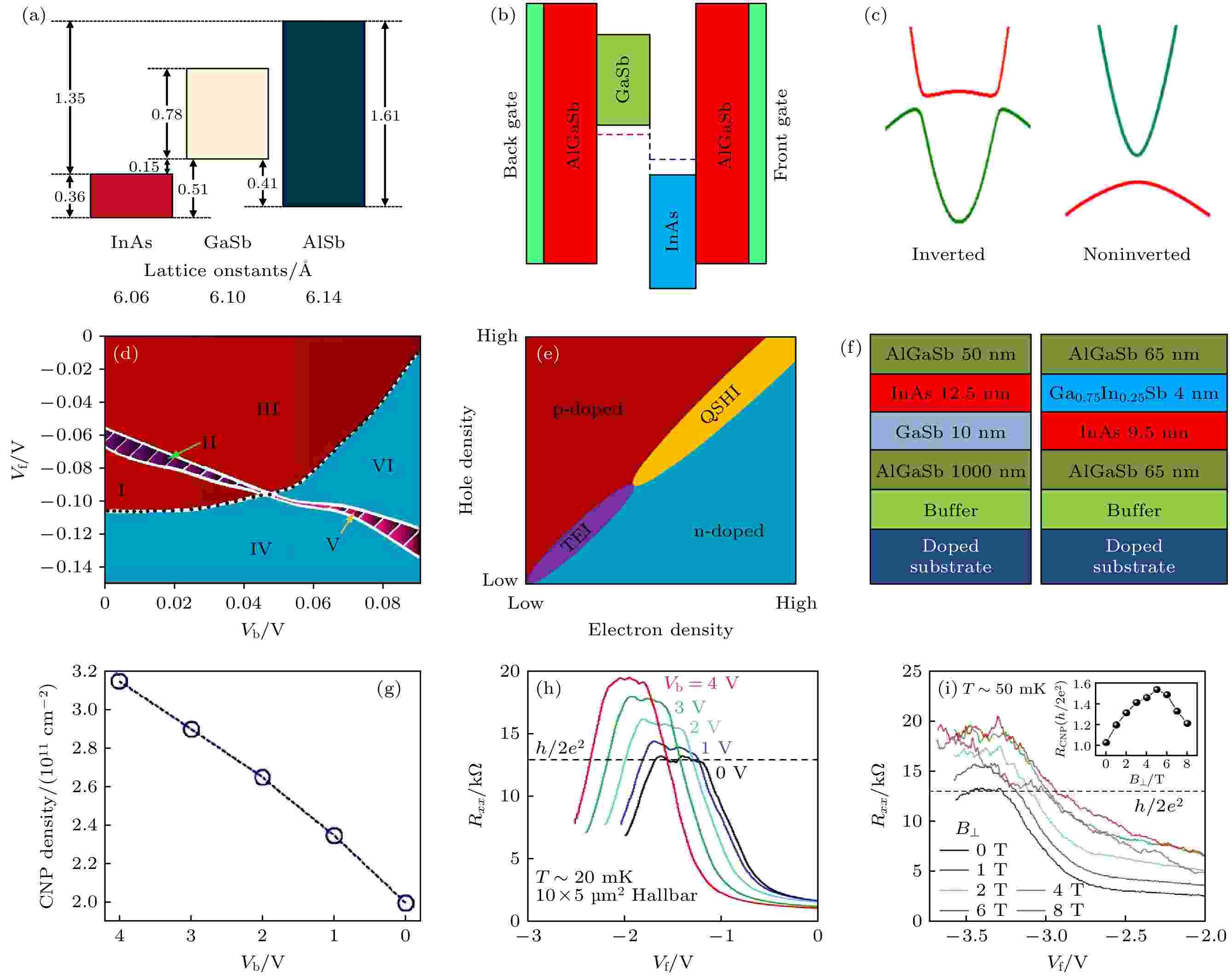
Under Coulomb interactions, electrons and holes have a phase transition from a semi-metal state into an excitonic ground state, with a gap spontaneously opening at the Fermi level. The excitonic ground state is called excitonic insulator. The excitonic insulator has attracted extensive attention in condensed matter physics, but the experimental evidence of such a quantum state is still under search. Until recent years, optical spectral and transport evidence of the excitonic insulator has first been observed in shallowly inverted InAs/GaSb quantum wells, which confirms the existence of the exciton insulator in a two-dimensional system. Surprisingly, one-dimensional helical-like topological edge states, which are not sensitive to temperature nor magnetic field, have been observed in the excitonic insulator state by transport measurements. This new quantum phase cannot be well explained by existing single-particle theories, which is called a topological excitonic insulator. In this paper, we systematically review the experimental studies on the topological excitonic insulator in the InAs quantum well and GaAs quantum well, including magneto transport, terahertz transmission, capacitance, and Coulomb drag measurements. These experimental results comprehensively characterize the bulk properties and edge properties of the topological excitonic insulator. Furthermore, as a ground state consisting of bosons, the topological excitonic insulator is expected to have a quantum phase transition into Bose-Einstein condensate with macroscopic coherence under extreme conditions, which provides a new platform for studying the quantum phenomena of Coulomb interactions in low dimensions.

2023, 72 (17): 177103.
doi: 10.7498/aps.72.20230995
Abstract +
In recent years, more and more magnetic topological materials, especially magnetic Weyl semimetals, have been discovered, providing a platform for studying the electronic transport behavior. The strong Berry curvature of magnetic topological materials can significantly enhance the conventional transverse transport behaviors, and can also make the transport phenomena that have been overlooked or unobserved appear gradually. In this review, the semi-classical equation is used to understand the anomalous transport behaviors in magnetic topological materials. The intrinsic anomalous Hall conductivity is obtained by integrating the Berry curvature of the occupied states, which is determined by the electronic band structure. The topological electronic state can be modulated by magnetic field and doping, and the anomalous Hall conductivity was changed with the evolution of the Berry curvature. A linear positive magnetoresistance behavior associated with the Berry curvature and magnetic field is introduced, which establishes the relation between the Berry curvature and the longitudinal transport. Due to the presence of tilted Weyl cone, the conductivity terms related to the first power of magnetic field are observed in magnetic Weyl systems. These behaviors under the interaction of topology and magnetic provide a new understanding and insight for the electric transport behaviors. At last, this review also provides a viewpoint on the field of magnetic topological physics.
2023, 72 (17): 177302.
doi: 10.7498/aps.72.20230698
Abstract +
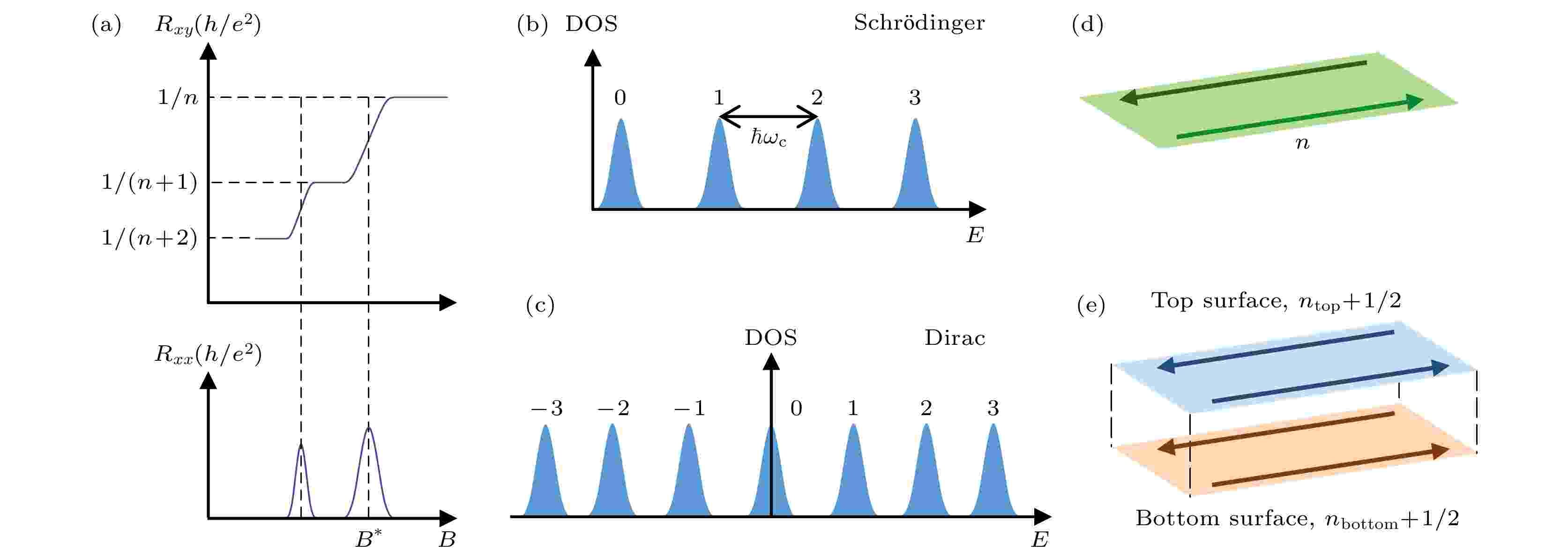
Three-dimensional topological insulators (TIs) with gapless topological surface states (TSSs) have attracted considerable attention because of their unique properties. The transport of TSS is an essential means to explore the novel properties. The quantum Hall effect (QHE) of TSS is an important content in the study of topological insulator, for it is an important characteristic of the pure TSS transport. This paper briefly reviews the recent research progress of QHE in TIs. Firstly, we introduce the fundamental concepts of the QHE in TIs. In a three-dimensional TI, each TSS contributes to a half-integer QHE. An integer QHE should be observed due to the existence of top and bottom surface in TI. Then, we review the realization and development of QHE. With the optimization of TI materials, the QHE of TSS is observed in bulk-insulating TIs. Next, the phase transition and scaling law behavior of QHE in TIs are discussed. The dominance of electron-electron interaction of the TSS is revealed by the anomalous critical exponent. Also, the experimental studies of the magnetic proximity and gate voltage modulation of the QHE are reviewed in detail. Finally, the perspectives of QHE in TIs are discussed.

2023, 72 (17): 177303.
doi: 10.7498/aps.72.20230672
Abstract +
Dirac quantum materials comprise a broad category of condensed matter systems characterized by low-energy excitations described by the Dirac equation. These excitations, which can manifest as either collective states or band structure effects, have been identified in a wide range of systems, from exotic quantum fluids to crystalline materials. Over the past several decades, they have sparked extensive experimental and theoretical investigations in various materials, such as topological insulators and topological semimetals. The study of Dirac quantum materials has also opened up new possibilities for topological quantum computing, giving rise to a burgeoning field of physics and offering a novel platform for realizing rich topological phases, including various quantum Hall effects and topological superconducting phases. Furthermore, the topologically non-trivial band structures of Dirac quantum materials give rise to plentiful intriguing transport phenomena, including longitudinal negative magnetoresistance, quantum interference effects, helical magnetic effects, and others. Currently, numerous transport phenomena in Dirac quantum materials remain poorly understood from a theoretical standpoint, such as linear magnetoresistance in weak fields, anomalous Hall effects in nonmagnetic materials, and three-dimensional quantum Hall effects. Studying these transport properties will not only deepen our understanding of Dirac quantum materials, but also provide important insights for their potential applications in spintronics and quantum computing. In this paper, quantum transport theory and quantum anomaly effects related to the Dirac equation are summarized, with emphasis on massive Dirac fermions and quantum anomalous semimetals. Additionally, the realization of parity anomaly and half-quantized quantum Hall effects in semi-magnetic topological insulators are also put forward. Finally, the key scientific issues of interest in the field of quantum transport theory are reviewed and discussed.
2023, 72 (17): 177401.
doi: 10.7498/aps.72.20230951
Abstract +
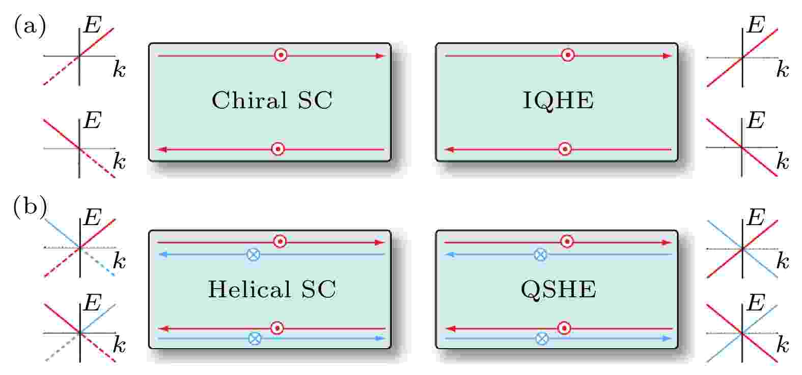
Topological superconductors have attracted much research interest, because they were proposed to host non-abelian Ising Anyon Majorana zero modes and thus can be used to construct fault-tolerant topological quantum computers. This paper mainly reviews the electrical transport methods for detecting the presence of Majorana zero modes. First, the basic concepts of topological superconductivity, Majorana zero modes and non-Abelian statistics are introduced, followed by a summary of various schemes for implementing topological superconductivity. Then, the experimental methods for detecting topological superconductivity or Majorana zero modes by using low-temperature transport methods, including electron tunneling spectroscopy, Coulomb blockade spectroscopy and non-local conductance detection, which are widely used in superconductor/nanowire hybrid systems, are discussed. On the other hand, the measurements of the (inverse) AC Josephson effect and current (energy) phase relationships are also reviewed to identify Majorana zero modes in Josephson devices. Meanwhile, to deepen our understanding of Majorana zero modes, some mechanisms for explaining the experimental data observed in the above experiments are provided. Finally, a brief summary and outlook of the electrical transport methods of Majorana zero modes are presented.
2023, 72 (17): 177202.
doi: 10.7498/aps.72.20230811
Abstract +
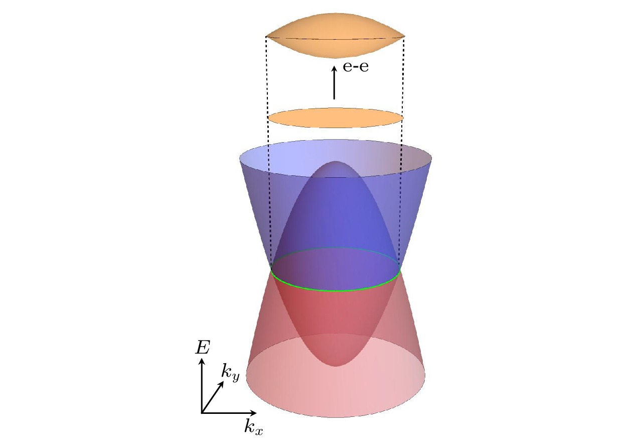
The topological nodal-line semimetal is characterized by the conduction band and valence band of electrons crossing along a one-dimensional line or closed loop in reciprocal space, with each nodal line carrying Π Berry phase. According to bulk-boundary correspondence, there exist drumheadlike surface states with weak dispersion at the boundary of system, surrounded by the projection of nodal loops onto the surface Brillouin zone. In most of nodal-line semimetals, the spin orbit coupling effect is weak, leading to the absence of a spin configuration for surface states under the single-particle picture. However, the featured weak dispersion of drumheadlike surface states enhances the electron-electron interaction effect, which triggers out ferromagnetic instability and causes spin splitting in the surface state. In this work, spin-dependent scattering caused by ferromagnetic surface states in spin-degenerate nodal-line semimetals is considered. It is found that both spin-splitting drumheadlike surface states can lead to resonant spin-flipped reflection. This physical process is reflected in a double-peak structure in the spin conductance spectrum. Specifically, we deal with the scattering problem induced by surface states in normal metal and nodal-line semimetal heterojunctions by using the scattering matrix and the Green’s functions theory, respectively, and obtain consistent conclusions. The result points out that spin-degenerate nodal-line semimetal surface states can still lead to spin-dependent transport, which provides a new perspective for the detection and potential application of spintronics in nodal-line semimetals.
SPECIAL TOPIC — Quantum transport in topological materials and devices • COVER ARTICLE
COVER ARTICLE
2023, 72 (17): 177301.
doi: 10.7498/aps.72.20230690
Abstract +
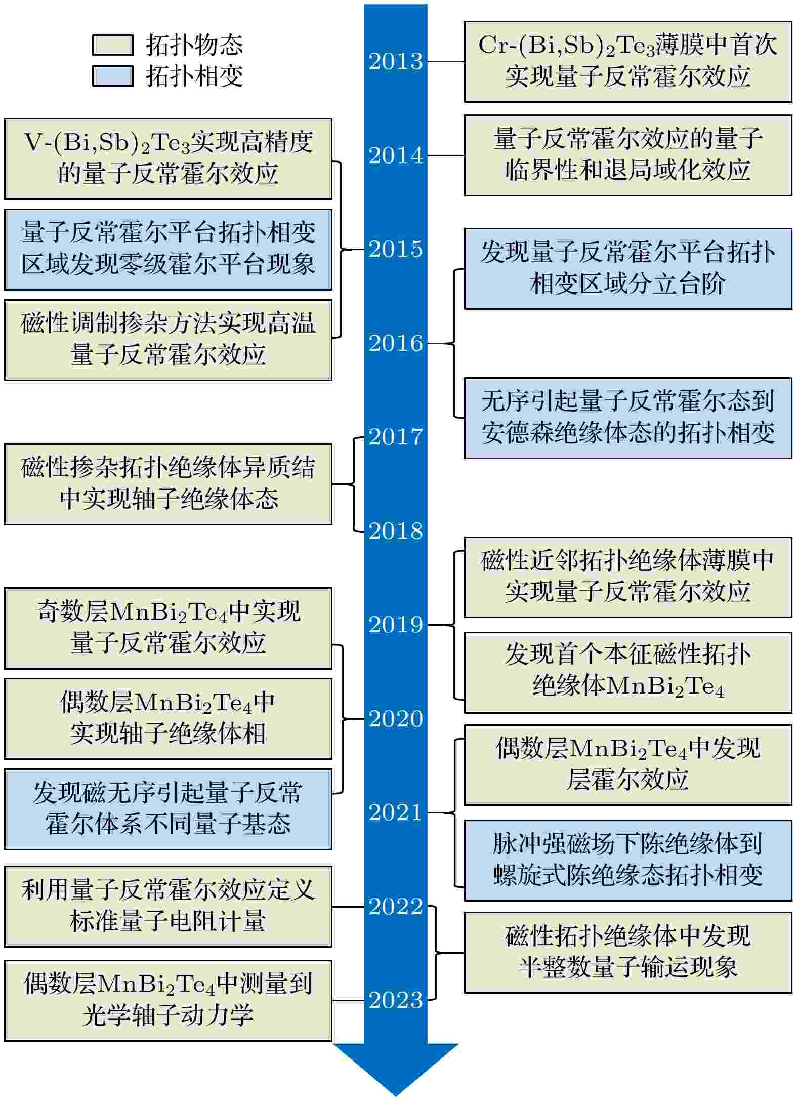
In the past decade, magnetic topological insulators have been an important focus in condensed matter physics research. The intricate interplay between the nontrivial band topology and spin, orbit, charge, and dimensionality degrees of freedom can give rise to abundant exotic topological quantum states and topological phase transitions. Measuring the transport properties of magnetic topological insulators is a crucial approach to exploring their exotic properties, which is of significant scientific importance in deepening our understanding of topological quantum states. Simultaneously, it also holds substantial potential applications in the development of novel low-power electronic devices. In this work, experimental progress of transport researches of magnetic topological insulators is reviewed, including quantum anomalous Hall effect and topological quantum phase transitions in magnetically doped topological insulators, the quantum anomalous Hall phase, axion insulator phase and Chern insulator phase in intrinsic antiferromagnetic topological insulator MnBi2Te4, as well as the helical phase emerged from the Chern insulator in pulsed high magnetic fields. Finally, this work analyzes the future direction of development in magnetic topological insulators, and the transport phenomena that have not been understood in these systems, offering an insight into and perspectives on the potential breakthroughs to be achieved in this area of research.
SPECIAL TOPIC—The 70th anniversary of National University of Defense Technology
EDITOR'S SUGGESTION
2023, 72 (17): 174202.
doi: 10.7498/aps.72.20230729
Abstract +
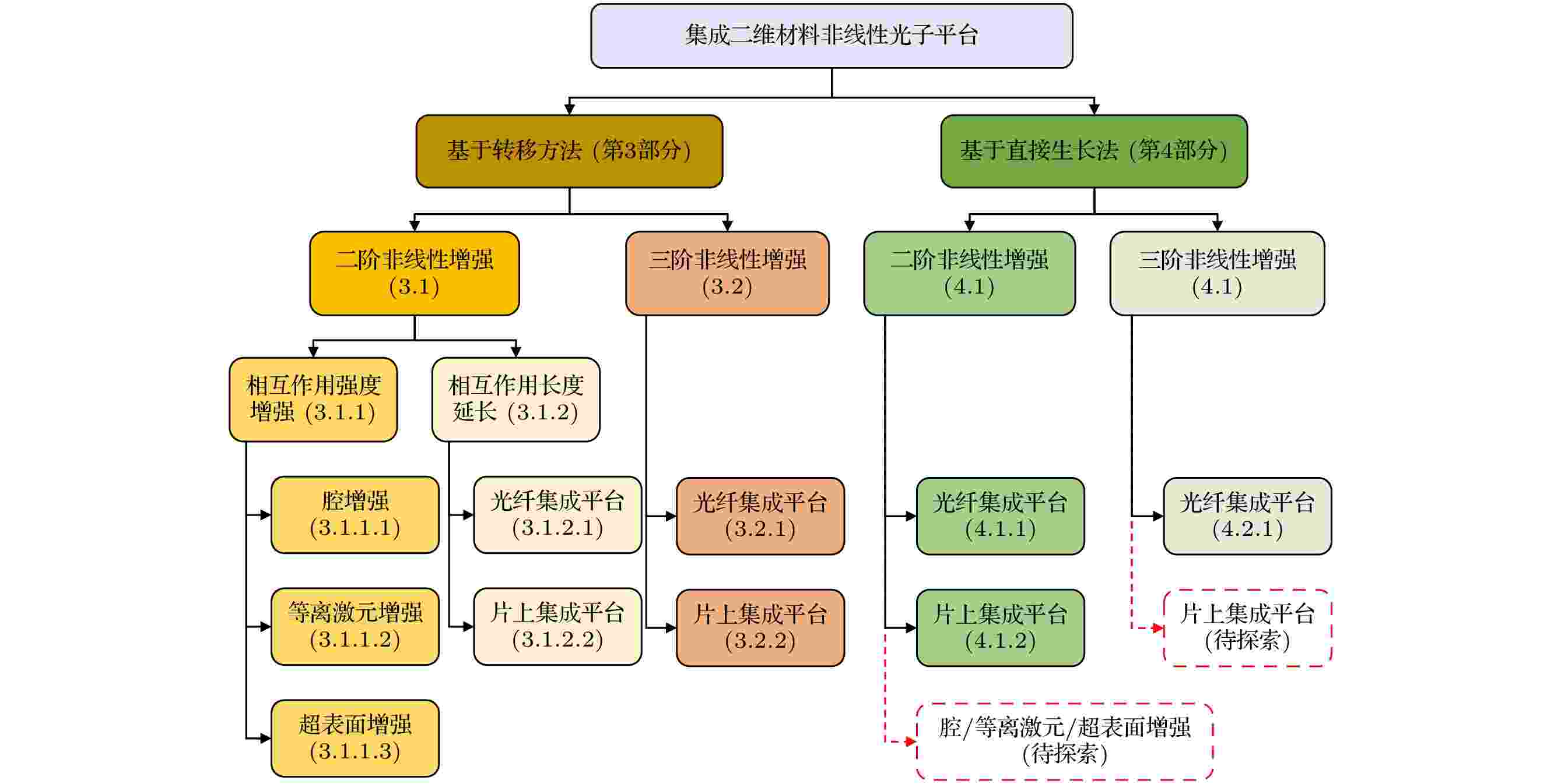
Photonic platforms with excellent nonlinear optical characteristics are very important to improve the devices' performance parameters such as integration, modulation speeds and working bandwidths for all-optical signal processing. The traditional processing technology of photonic platforms based on silicon, silicon nitride and silicon oxide is mature, but the nonlinear function of these optical platforms is limited due to the characteristics of materials; Although two-dimensional (2D) materials possess excellent nonlinear optical properties, their nonlinear potentials cannot be fully utilized because of their atomic layer thickness. Integrating 2D materials with mature photonic platforms can significantly improve the interaction between light and matter, give full play to the potentials of 2D materials in the field of nonlinear optics, and improve the nonlinear optical performances of the integrated platforms on the basis of fully utilizing the mature processing technology of the photonic platforms. Based on the above ideas, starting from the basic principle of nonlinear optics (Section 2), this review combs the research progress of various nonlinear photonic platforms (resonators, metasurfaces, optical fibers, on-chip waveguides, etc.) heterogeneously integrated with 2D materials, realized by traditional transfer methods (Section 3) and emerging direct-growth methods (Section 4) in recent years, and the introduction is divided into second-order and third-order nonlinearity. Comparing with the transfer methods, the advantages of using direct-growth methods to realize the heterogeneous integration of 2D materials and photonic platforms for the study of nonlinear optics are expounded, and the technical difficulties to be overcome in preparing the actual devices are also pointed. In the future, we can try to grow 2D materials directly onto the surfaces of various cavities to study the enhancement of second-order nonlinearity; we can also try to grow 2D materials directly onto the on-chip waveguides or microrings to study the enhancement of third-order nonlinearity. Generally speaking, the research on integrated nonlinearity by directly growing 2D materials onto various photonic structures has aroused great interest of researchers in this field. As time goes on, breakthrough progress will be made in this field, and technical problems such as continuous growth of high-quality 2D materials onto photonic structures and wafer-level large-scale preparation will be broken through, further improving the performance parameters of chips and laying a good foundation for optical communication, signal processing, optical sensing, all-optical computing, quantum technology and so on.
REVIEW
EDITOR'S SUGGESTION
2023, 72 (17): 178701.
doi: 10.7498/aps.72.20230733
Abstract +
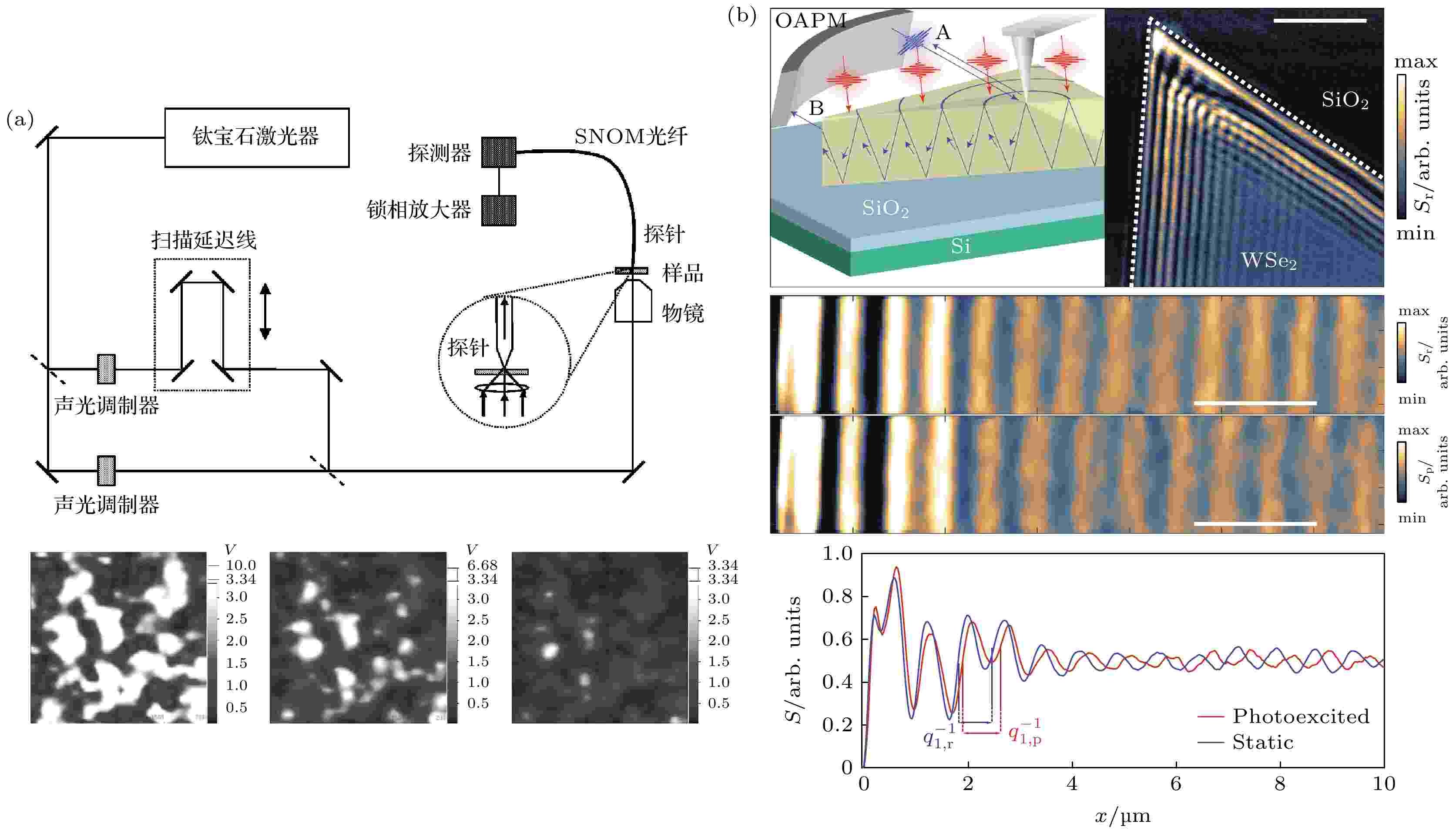
High-resolution microscopy has opened the door to the exploration of the micro-world, while femtosecond laser has provided a measurement method for detecting ultrafast physical/chemical phenomena. Combination of these two techniques can produce new microscopic techniques with both ultra-high spatial resolution and ultra-fast temporal resolution, and thus has great importance in exploring new scientific phenomena and mechanisms on an extremely small spatial scale and temporal scale. This paper reviews the basic principles and properties of main microscopic techniques with ultra-high temporal resolution and spatial resolution, and introduces the latest research progress of their applications in various fields such as characterizing optoelectronic materials and devices, monitoring femtosecond laser micromachining, and detecting surface plasmon excitation dynamics. In order to conduct these researches systematically, we group these techniques based on time dimension and space dimension, including the near-field multi-pulse imaging techniques, the far-field multi-pulse imaging techniques, and the far-field single-pulse imaging techniques. In Section 2, we introduce the principles and characteristics of the ultra-high spatiotemporally resolved microscopic techniques. The near-field multi-pulse spatiotemporally microscopic techniques based on nano-probe are described in Subsection 2.1, in which is shown the combination of common near-field imaging techniques such as atomic force microscopy (AFM), near-field scanning optical microscopy (NSOM), scanning tunneling microscope (STM), and the ultra-fast temporal detection of pump-probe technique. In Subsection 2.2, we introduce the far-field multi-pulse spatiotemporal microscopic techniques. In contrast to near-field cases, the far-field spatiotemporal microscopic techniques have lower spatial resolution but possess more advantages of being non-invasive and non-contact, wider field of view, and faster imaging speed. In Subsection 2.3 we introduce the far-field single-pulse spatiotemporal microscopic techniques, in which is used a single ultrafast light pulse to capture dynamic processes at different moments in time, thereby enabling real-time imaging of ultrafast phenomena. In Section 3 , the advances in the application of the ultra-high spatiotemporal resolved microscopic techniques are introduced in many frontier areas, including the monitoring of femtosecond laser micromachining in Subsection 3.1, the detection of optoelectronic materials/devices in Subsection 3.2, and the characterization of surface plasmon dynamics in Subsection 3.3. Finally, in Section 4, we summarize the features of all above-mentioned spatiotemporal microscopic techniques in a table, including the spatial resolution and temporal resolution, advantages and disadvantages of each technique, and we also provide an outlook on future development trend in this research field. Looking forward to the future, ultra-high spatiotemporally resolved microscopy will develop rapidly toward the goal of "smaller, faster, smarter and more extensive". Its development not only promotes the research of the microscopy technology, but also provides a powerful tool for various practical applications such as precision machining, two-dimensional material dynamics, optoelectronic device design and characterization.
GENERAL

2023, 72 (17): 170301.
doi: 10.7498/aps.72.20230589
Abstract +
Isometric tensor offers a novel and powerful tool that can compress an entangled state into its tensor network state (TNS). The resulting quantum compression provides a new opportunity for enhancing quantum key distribution (QKD) protocols. The main idea explored in this work is to use the quantum compression to improve the efficiency of QKD. In a nut-shell, a collection of any multi-photon entangled states that carry encoded classical bits is compressed into a single-photon state before the corresponding photon is sent to the receiver that measures the qubit and decompresses it. In this paper, we first show how to obtain the generalized isometric tensors for compressing any entangled states and their inverse isometric tensors for decompression. In our proposed QKD protocol, the input state consists of any multi-photon entangled states, which are first compressed into a single-photon state $ \left| 0 \right\rangle $ or $ \left| 1 \right\rangle $ or Bell states by the sender Alice. A sequence of single-photon states $ \left| 0 \right\rangle $ and $ \left| 1 \right\rangle $ and one photon from the Bell state mixed with decoy qubits is sent to the receiver Bob via a quantum channel. Bob obtains the final sifted compressed states $ \left| 0 \right\rangle $ and $ \left| 1 \right\rangle $ and conjugate transpose of the isometric tensors. Using our protocols, Bob can decompress the received states $ \left| 0 \right\rangle $ and $ \left| 1 \right\rangle $ into original entangled states. Since quantum processors that are used to send quantum information between nodes are relatively primitive and low in power and the preparation of many-photon entanglement is relatively difficult at present, finding suitable protocols for the compression of transmitted quantum data brings important practical benefits. More generally, the quantum information theory primarily investigates quantum data manipulation under locality constraints, so our protocols connect naturally to these investigations. Our protocols increase the encoding capacity of QKD protocols. Not only our proposed processes of compression and decompression are very simple, but also entanglement compression using isometric tensors can be implemented by using quantum circuits and current technology. Because many ideas for designing of quantum information processing equipment envision that a network composed of relatively small quantum processors sending quantum information between nodes, it is greatly significant to find appropriate protocols for compressing the transmitted quantum data .
2023, 72 (17): 170302.
doi: 10.7498/aps.72.20230625
Abstract +
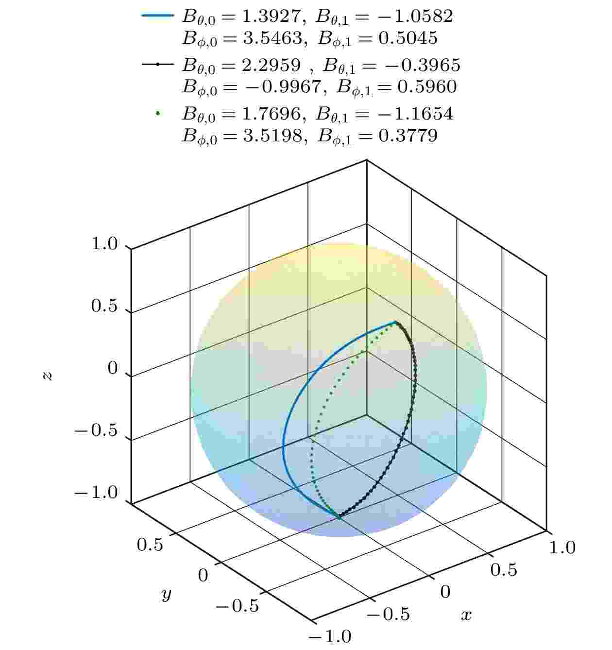
Quantum computing is a new way to process quantum information by using superposition and entanglement of the quantum system. Quantum state’s vast Hilbert space allows it to perform operations that classical computers cannot. The quantum computing has unique advantages in dealing with some complex problems, so it has attracted wide attention. Computing a single qubit is the first of seven fundamental stages needed to achieve a large-scale quantum computer that is universal, scalable and fault-tolerant. In other words, the primary task of quantum computing is the careful preparation and precise regulation of qubits. At present, the physical systems that can be used as qubits include superconducting qubits, semiconductor qubits, ion trap systems and nitrogen-vacancy (NV) color centers. These physical systems have made great progress of decoherence time and scalability. Owing to the vulnerability of qubits, ambient thermal noise can cause quantum decoherence, which greatly affects the fidelity of qubits. Improving the fidelity of qubits is therefore a key step towards large-scale quantum computing. Based on the dipole field driven qubit, the stochastic dynamic structure decomposition method is adopted and the Kubo-Einstein fluctuation-dissipation theorem is used to study the qubit control in a thermal noise environment. The dipole field has components in three directions, not just in one plane, which allows more flexible control of quantum states. Without considering the noise, the quantum state can reach the target state 100%. In the noisy environment, thermal noise will cause the deviation between the actual final state and the target final state caused by thermal fluctuation, which becomes the main factor affecting the quantum fidelity. The influence of thermal noise is related to temperature and the evolution trajectory of quantum state. Therefore, this paper proposes an optimal scheme to improve the qubit fidelity in the thermal noise environment. The feasibility of this method is verified by numerical calculation, which can provide a new solution for further guiding and evaluating the experiment. The scheme is suitable for qubit systems of various physical control fields, such as semiconductor qubits and nitrogen vacancy center qubits. This work may have more applications in the development of quantum manipulation technology and can also be extended to multi-qubit systems, the details of which will appear in the future work.
2023, 72 (17): 170501.
doi: 10.7498/aps.72.20230642
Abstract +
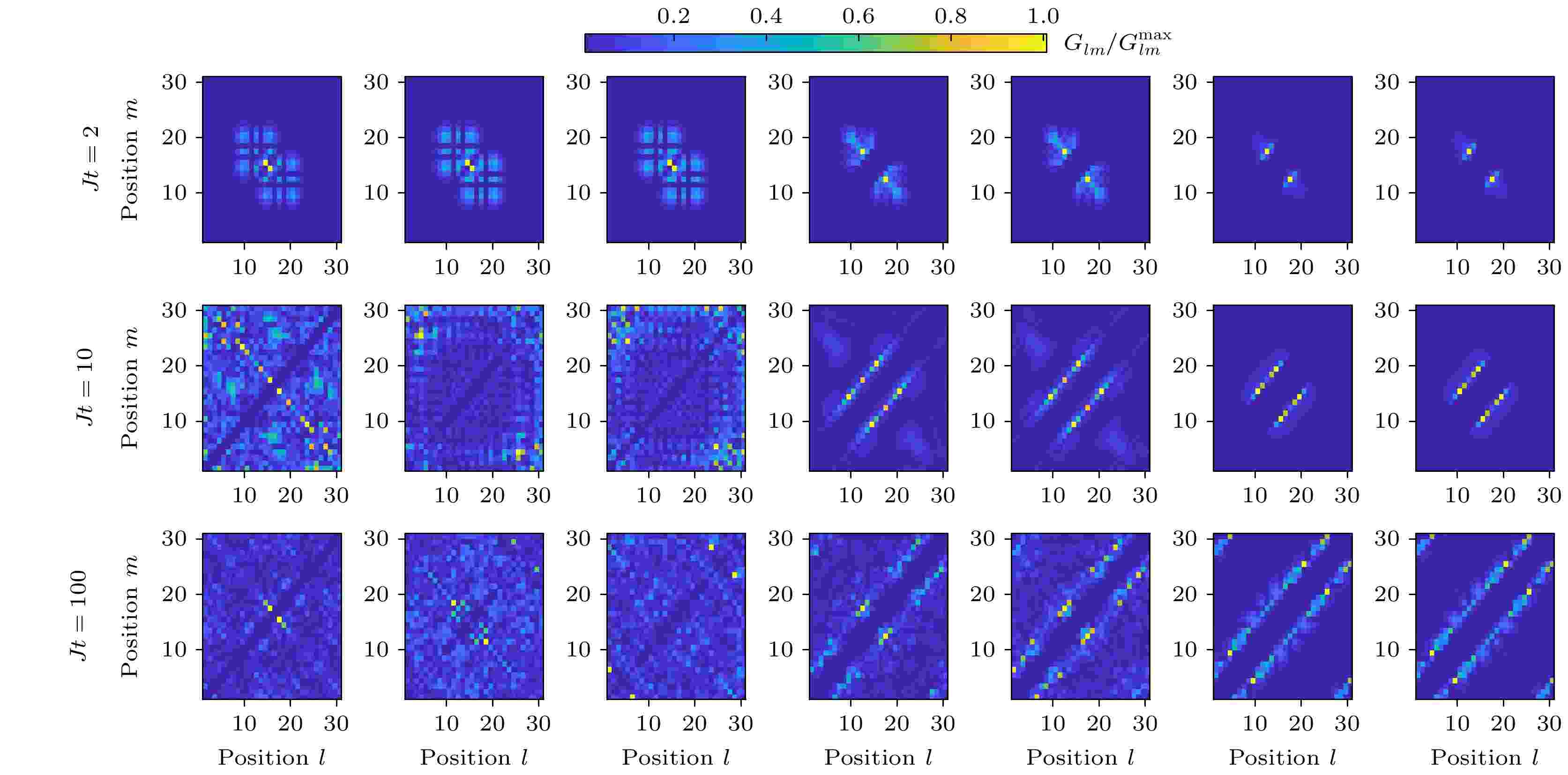
The quantum walk of two hard-core bosons in one-dimensional lattice under the effect of long-range inter-particle interaction is studied in detail. We also simulate the influence of an isolated defect that may exist in the lattice on the quantum walk of two particles by adding an additional potential energy to a certain lattice site. Using exact diagonalization method, the continuous-time quantum walk is directly simulated. The numerical simulations show that the range of interaction (long-range or short-range), the strength of the inter-particle interaction, the initial state of the two particles and the presence of the isolated defect have great influences on the quantum walk. Under the effect of strong long-range interaction, the particles initially located on the non-adjacent lattice sites have a co-walking behavior, while under the short-range interactions (nearest-neighbor interactions) only two particles initially located on the neighboring lattice sites can exhibit co-walking. After introducing the isolated defect into the system with strong interaction, two particles residing on the same side of the isolated defect keep co-walking, while two particles located on either sides of the isolated defect or one particle located on the isolated defect and the other particle staying on the side of the isolated defect, the two particles keep stationary or co-walking near the defect, displaying the characteristics of localization. By using the second-order perturbation theory of degenerate quantum system, a comprehensive theoretical analysis of the above numerical results is given. The theoretical analysis reveals the underlying physical law of quantum walks of two particles in one-dimensional lattice under the effects of strong long-range interaction and isolated defect in the lattice.
ATOMIC AND MOLECULAR PHYSICS

2023, 72 (17): 173201.
doi: 10.7498/aps.72.20230739
Abstract +
Curcumin (CUR) is a commonly used pharmaceutical with anti-inflammatory, antioxidant and anti-cancer effects, but its solubility in water is relatively low. In recent years, pharmaceutical co-crystal has been an effective method of enhancing the solubility of limited water-soluble pharmaceuticals. Based on this, terahertz time-domain spectroscopy (THz-TDS) is used to study the THz spectra of curcumin-catechol co-crystal. Firstly, the experimental spectra of curcumin, catechol (CTL), their physical mixture and their co-crystal are measured in a range of 0.5–3.5 THz, respectively. The experimental data show that CUR obtains six THz absorption peaks, while CTL possess three THz absorption peaks, the physical mixture obtains four absorption peaks, and their CUR-CTL co-crystal obtains three absorption peaks. These results indicate that THz-TDS can effectively identify curcumin, catechol and their co-crystals. The fact that the absorption peak at 3.31 THz obtained in co-crystal is entirely different from those of raw materials, implying that new weak interactional forces are generated between CUR molecule and CTL molecule, the co-crystal forms a new three-dimensional structure compared with their raw materials. These results are also verified by X-ray diffraction spectra of raw material and their Co-crystal. Moreover, four possible theoretical forms of curcumin-catechol co-crystal are optimized and simulated by using density functional theory (DFT). The calculated results indicate that the data of co-crystal form III are in good agreement with the experimental spectrum, and the simulation effectively reconstructs the experimental spectrum. So it can be inferred that the co-crystal is formed through the hydrogen bond between the carbonyl C10=O3 of CUR and the hydroxy O61-H55 of CTL. In addition, depending on the good match between experimental data and theoretical results, it is found that the three absorption peaks in the co-crystal do not origin from the action of a single molecule, but the joint action of the functional groups of the two molecules under the driving by the hydrogen bond. The existence of weak interaction forces, such as the hydrogen bond, not only changes the structural parameters of the two molecules, but also reestablishes a new intermolecular force, which then affects the interactional motions of the co-crystal. This fact directly leads the CUR-CTL co-crystal to exhibit THz absorption peaks different from those of raw materials in the THz band.
ELECTROMAGNETISM, OPTICS, ACOUSTICS, HEAT TRANSFER, CLASSICAL MECHANICS, AND FLUID DYNAMICS

2023, 72 (17): 174201.
doi: 10.7498/aps.72.20230499
Abstract +
The scattering measurement of particulates in gaseous medium is helpful in understanding light transmission, laser detection, combustion radiation and atmospheric environment. In order to explore the scattering characteristics of micron-/nano-sized particles, this paper proposes a method of accurately measuring the scattering intensity distribution of a single micron-sized particles/nanoclusters by combining laser levitation and scattering measurement. An experimental apparatus is first built based on the counter-propagated bi-Bessel beams levitation system and scattering test system. The microparticles/nanoclusters of various matters and sizes are then levitated and their stabilities are evaluated. Finally, the scattering intensity distribution of levitated particles within 2π scattering angle is accurately measured with an angular resolution of 9.2″. The forces acting on particles under laser irradiation and the scattering intensity distribution of different particle parameters are simulated and calculated, and compared with experimental results. The influence of noise on the uncertainty of the scattering measurement system is analyzed in depth, including background light, laser beam, and reflected light from the walls. The results show that the signal-to-noise ratio of scattering measurement for metallic magnesium and aluminum, whether single particles or clusters, are both greater than 20 dB and their maximum values are both 94.6 dB in a range of 2π angle. For graphite nanoclusters, the signal-to-noise ratio in the backscattering direction is relatively poor. The influence of levitation instability on the scattering measurement results is estimated in detail, verifying that the influence of levitation instability in the test system on the scattering measurement is ignorable. Metallic magnesium, aluminum, and graphite particles can be stably levitated by the counter-propagated bi-Bessel beams, with a relative instability of less than 0.15. During the levitation, the photophoretic force plays a dominant role. The scattering intensity distribution of a single micron-sized particles and nanoclusters both conform to the scattering characteristics of Mie particles. Microparticles with large refractive index imaginary parts have stronger forward scattering characteristics. The larger the particle size parameter, the stronger the forward scattering effect becomes. The accurate measurement of the scattering intensity distribution of a single microparticles confirms the versatility and reliability of the levitation scattering test system, providing a new research method for in-depth understanding of the scattering characteristics of substances.
2023, 72 (17): 174203.
doi: 10.7498/aps.72.20230807
Abstract +
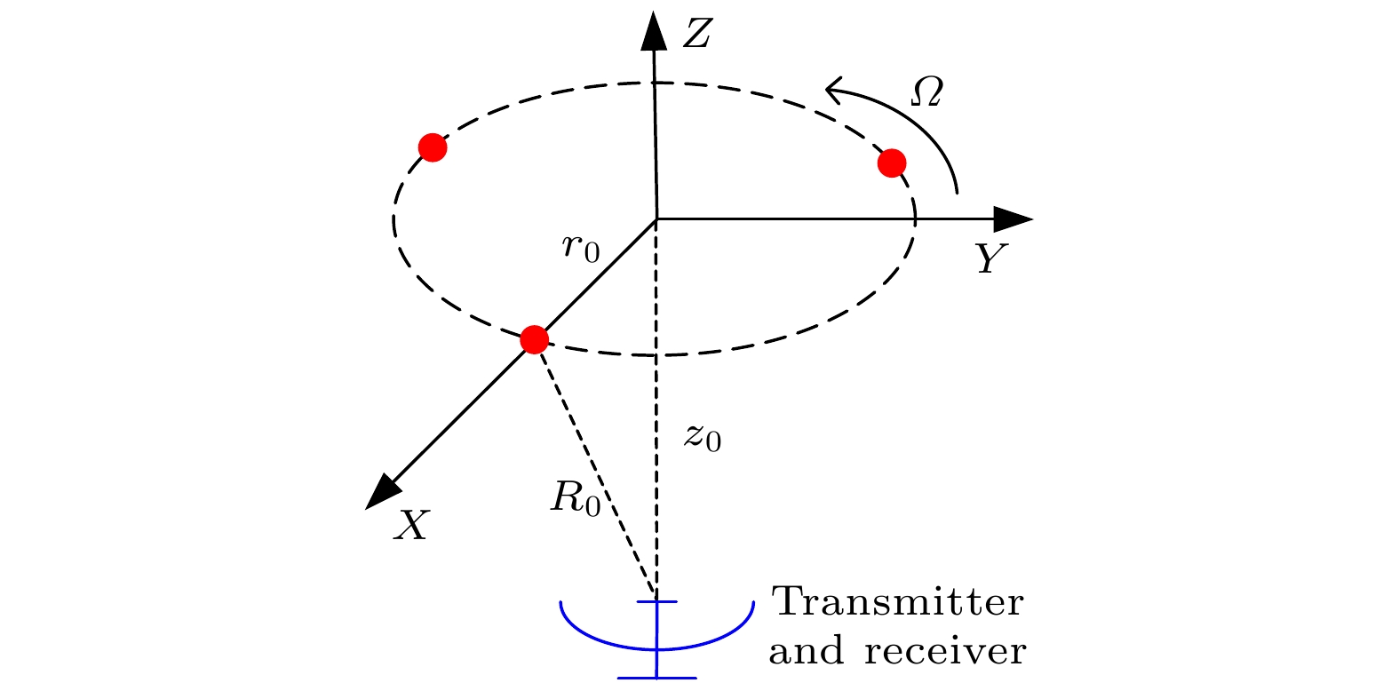
Rotational Doppler effect is an important phenomenon when the vortex electromagnetic wave carrying orbital angular momentum is used to detect a rotating target. Compared with the traditional plane wave case, rotational Doppler effect enables the vortex electromagnetic wave to detect the spin motion along the rotation axis of target. However, there are still some blind zones when the integer orbital angular momentum beams are used to detect specific spinning objects. To expand the application scope of detection scheme based on the rotational Doppler effect, according to the time-frequency analysis, in this paper we study the method of estimating the rotation speed of spinning objects under the normal incidence and oblique incidence of fractional orbital angular momentum beams. Firstly, based on the ideal scattering point model, the echo models are derived under the normal incidence and oblique incidence of integer orbital angular momentum beam and fractional orbital angular momentum beam, respectively, as well as theoretical time-frequency curves. Then taking the three-dimensional practical object for example, the echo under the incidence of fractional orbital angular momentum beams and its time-frequency graph are achieved by using the momentum method and short-time Fourier transform. The time-frequency ridge and its fluctuation period are extracted from the time-frequency graph, thereby estimating the spinning speed of target. The results show that the fractional orbital angular momentum beams can be used to estimate the rotation speed of spinning objects effectively, whether it is normal incidence or oblique incidence, thereby solving the problem about the detection blind zone of integer orbital angular momentum beams, and improving the applicability in detecting spin motion.
2023, 72 (17): 174204.
doi: 10.7498/aps.72.20230762
Abstract +
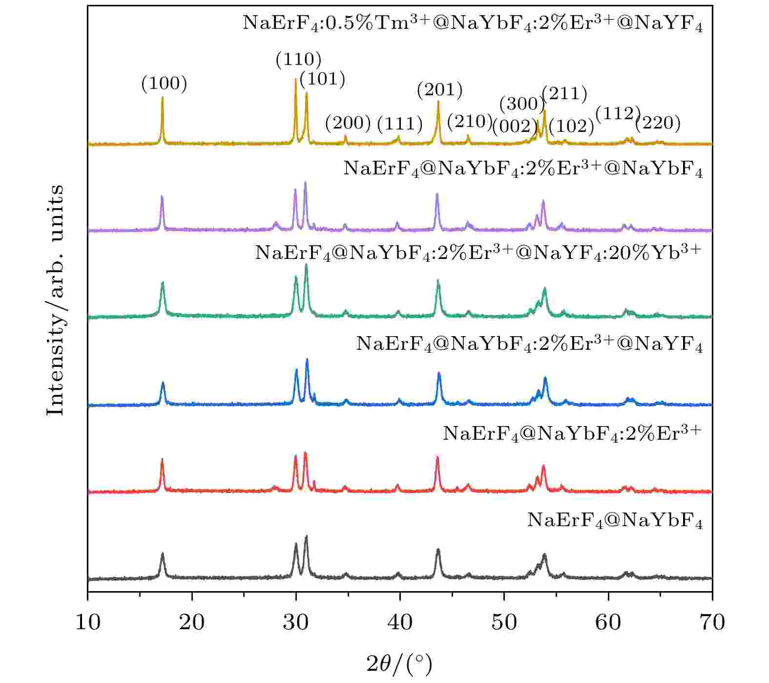
Building core-shell structures are widely used to enhance and regulate the luminescence properties of rare-earth-doped micro/nano materials. In this work, a variety of different NaErF4 core-shell and core-shell-shell nanocrystals are successfully constructed based on high temperature co-precipitation method by epitaxial growth technology. The upconversion red emission intensities of Er3+ ions in different core-shell structures are effectively enhanced by regulating their structures and doping ions. The experimental structures show that the constructed core-shell nanocrystals each have a hexagonal phase structure, and core-shell structure of about 40 nm. In the near infrared 980 nm laser excitation, the NaErF4 core-shell nanocrystal shows a strong single-band red emission. And the single-band red emission intensity of Er3+ ions is enhanced through constructing the NaErF4@NaYbF4:2%Er3+ core-shell structure. The experimental results show that red emission intensity of Er3+ ions is about 1.4 times higher than that of the NaErF4@NaYbF4 core-shell structure by constructing the NaErF4@NaYbF4:2%Er3+ core-shell structures under 980 nm excitation, and its red/green emission intensity ratio increases from 5.4 to 6.5. Meanwhile, when NaErF4@NaYbF4:2%Er3+ core-shell structure recoats the NaYF4 inert shell and is added with a small quantity of Tm3+ ions, their red emission intensities of Er3+ ions are 23.2 times and 40.3 times that of NaErF4@NaYbF4 core-shell structures, and their red/green emission intensity ratios reach 7.5 and 10.2, respectively. The red emission enhancement of Er3+ ions is mainly caused by bidirectional energy transfer process of high excitation energy of Yb3+ ions and energy trapping center of Tm3+ ions which effectively change the density of population of luminescent energy levels of Er3+ ions. Furthermore, the coated NaYF4 inert shell also effectively weakens the surface quenching effect of nanocrystals. The mechanisms of red enhancement in different core-shell structures are discussed based on the spectral properties, the process of interion energy transfer, and luminescence kinetics. The constructed NaErF4@NaYbF4:2%Er3+@NaYF4 core-shell structures with high-efficiency red emission in this work have great potential applications in the fields of colorful anti-counterfeiting, display and biological imaging.
2023, 72 (17): 174205.
doi: 10.7498/aps.72.20230394
Abstract +
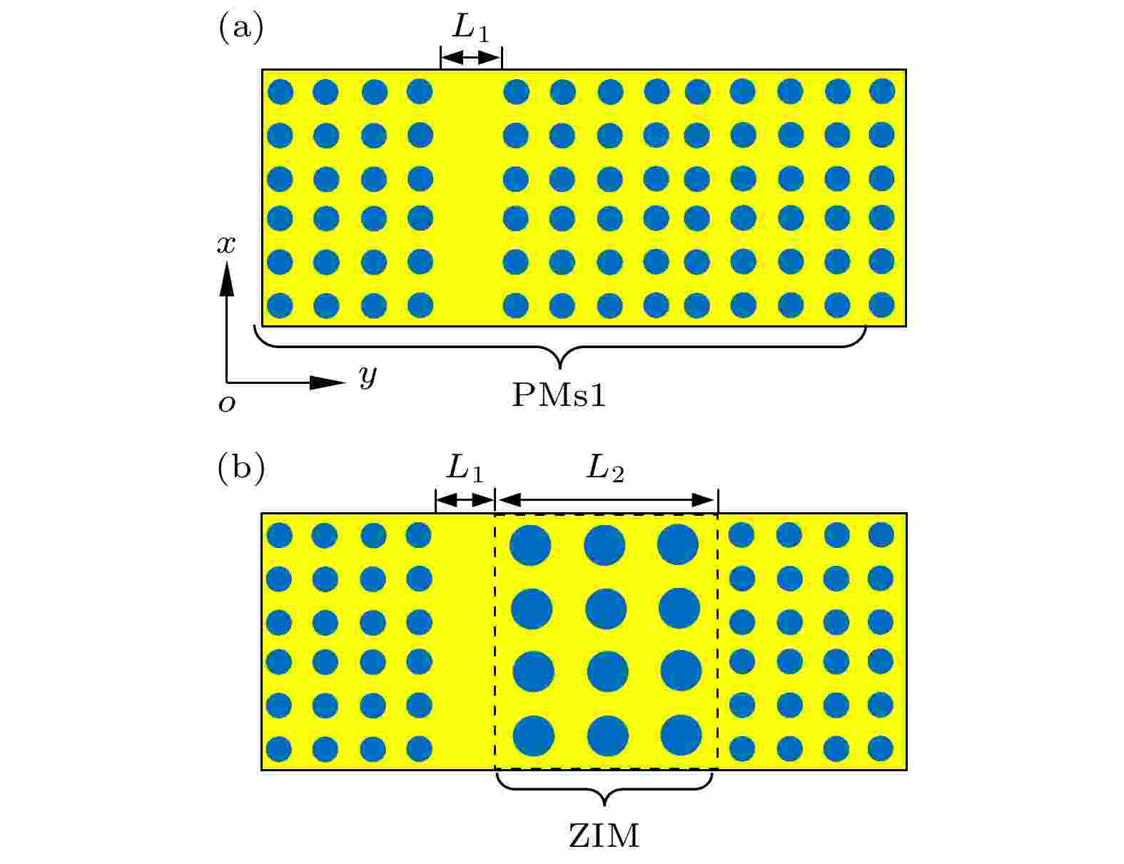
Owing to the photonic band gap effect and defect state effect, photonic metamaterials have received much attention in the design of narrow bandpass filters, which are the key devices of optical communication equipment such as wavelength division multiplexing devices. In this work, based on zero-index metamaterial (ZIM), a compact filter with both high peak transmission coefficient and ultra-narrow bandwidth is proposed. The photonic metamaterial with conical dispersion and Dirac-like point is achieved by optimizing the structure and material component parameters of dielectric rods with square lattice in air. It is demonstrated that a triply degenerate state can be realized at the Dirac-like point, which relates this metamaterial to a zero-index medium with effective permittivity and permeability equal to zero simultaneously. Electromagnetic (EM) wave can propagate without any phase delay at this frequency, and strong dispersion occurs in the adjacent frequency cone, leading to dramatic changes in optical properties. We introduce a ZIM into photonic metamaterial defect filter to compress the bandwidth to the realization of ultra-narrow bandpass filter. The ZIM is embedded into the resonant cavity of line defect filter, which is also composed of dielectric rods with square lattice in air. In order to increase the sensitivity of the phase change with frequency, the Dirac-like frequency is adjusted to match the resonant frequency of the filter. We study the transmission spectrum of the structure through the COMSOL Multiphysics simulation software, and find that the peak width at half-maximum of the filter decreases as the thickness of ZIM increases, and the peak transmittance is still high when bandwidth is greatly compressed. The zero phase delay inside the slab can be observed. Through field distribution analysis, the zero-phase delay and strong coupling characteristics of electromagnetic field are observed at peak frequency. The comparison with conventional photonic metamaterials filter is discussed. We believe that this work is helpful in investigating the realization of ultra-narrow bandpass filters.
EDITOR'S SUGGESTION
2023, 72 (17): 174206.
doi: 10.7498/aps.72.20230850
Abstract +
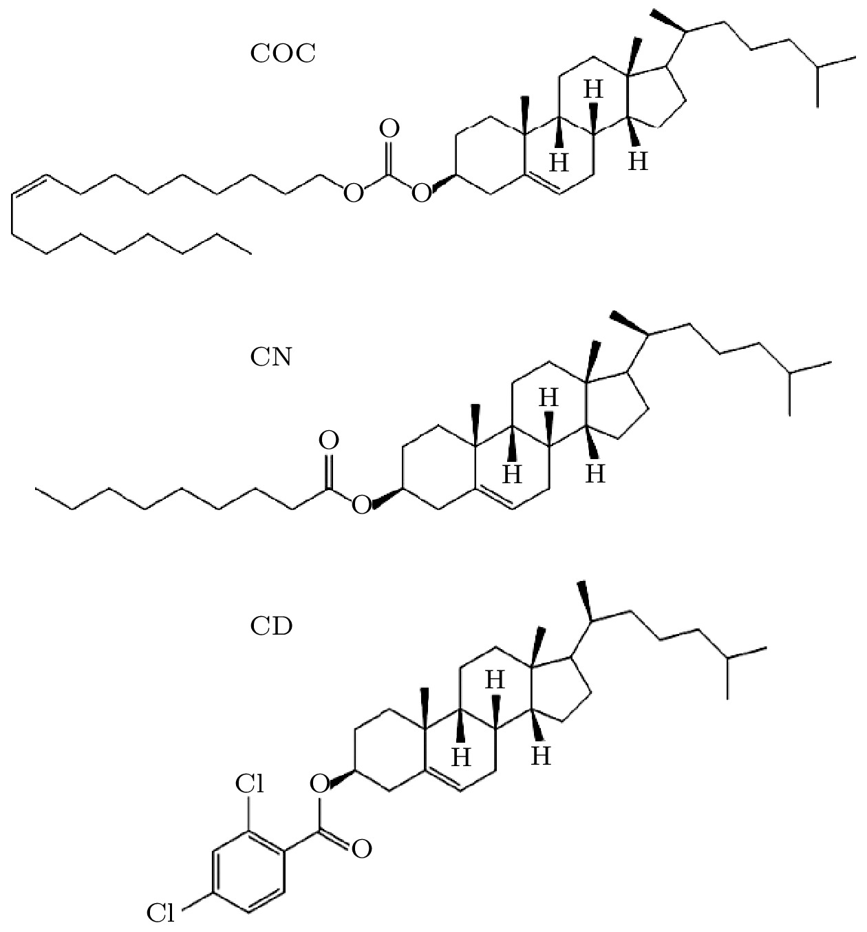
Modern anti-counterfeiting technology can effectively suppress and combat forgery and counterfeiting behaviors, which is of great significance in information security, national defense and economy. However, the realization of multi-dimensional, integrated, difficult-to-copy and easy-to-detect optical anti-counterfeiting devices is still a challenge. In this paper, a multi-dimensional and polarization-dependent anti-counterfeiting device with structure color is designed, which is composed of patterned liquid crystal polymer (LCP) nematic layer and thermotropic cholesteric liquid crystal (TLC) layer. It has the advantages of displaying and hiding polarization states, wide color tuning range, convenient operation, high integration and security. For incident light with a specific polarization state, the patterned nematic phase LCP layer can carry out regionalized phase editing and polarization state modulation, while the TLC layer can selectively reflect the incident light. Therefore, a patterned structural color security label is subtly realized. The anti-counterfeiting device can realize the display, hiding, color adjustment and image/background conversion of patterns by adjusting the polarization direction of incident light. In addition, the TLC layer in the device can meet the application requirements of the anti-counterfeit device at different environmental temperatures through the flexible design of the system weight ratio. Furthermore, the device can be easily heated by body temperature, realize dynamic real-time wide-spectrum color modulation and reversible pattern erasure, and further enhance its security dimension and security. The multi-polarization-type anti-counterfeiting device has three-dimensional anti-counterfeiting efficacy. The first dimensional anti-counterfeiting efficacy is achieved by the thermochromic liquid crystal layer. The thermochromic liquid crystal layer has no reflection color outside the operating temperature range of TLC material, and the entire device displays black background. The second and the third dimensional anti-counterfeiting efficacy are related to the polarization state of the incident light and the linear polarization direction, respectively. Only when the incident light is linearly polarized light and its polarization direction makes an angle of 45° or –45° with respect to the optical axis of the liquid crystal, will the device show the designed pattern. Consequently, our proposed anti-counterfeiting device is expected to provide a new idea for developing the anti-counterfeiting field.
PHYSICS OF GASES, PLASMAS, AND ELECTRIC DISCHARGES

2023, 72 (17): 175201.
doi: 10.7498/aps.72.20230680
Abstract +
Low frequency oscillation in the discharge channel of Hall thruster is an important physical phenomenon that affects its performance and stability. In this paper, the characteristics of low-frequency oscillation of the discharge current of Hall thruster and its suppression method are numerically studied by using a one-dimensional fluid model. Assuming that the discharge channel satisfies the quasi-neutral condition, the effects of electron-neutral collision, electron anomalous transport and electron-wall collision on conductivity are considered. The changes of plasma parameters and the effects of magnetic field, preionization rate, and atomic velocity on the amplitude and frequency of discharge current oscillation are also studied. Research results show that the variation of electron temperature in the discharge channel is closely related to the ionization process, and the electron temperature increases as the ionization intensity increases. The fluctuations in neutral gas flow rate and atomic density in the discharge process cause the ionization region to move forward and backward and the ionization intensity to change, which are the main driving forces for the low-frequency oscillation of discharge current in the channel. The magnetic field intensity in the discharge channel affects the axial current by influencing the electron mobility. With the increase of field strength, the oscillation frequency of current decreases, and under different magnetic field strengths, the current amplitude drops as the discharge voltage decreases. When the preionization rate of the working gas increases to above 4%, the amplitude of the discharge current oscillation gradually decreases. When the preionization rate is greater than 3% and the atomic velocity is less than 160 m/s, the discharge current oscillation in the channel exhibits damping attenuation, achieving a stabilizing effect which conduces to stabilizing the discharge of the Hall thruster.
2023, 72 (17): 175202.
doi: 10.7498/aps.72.20230514
Abstract +
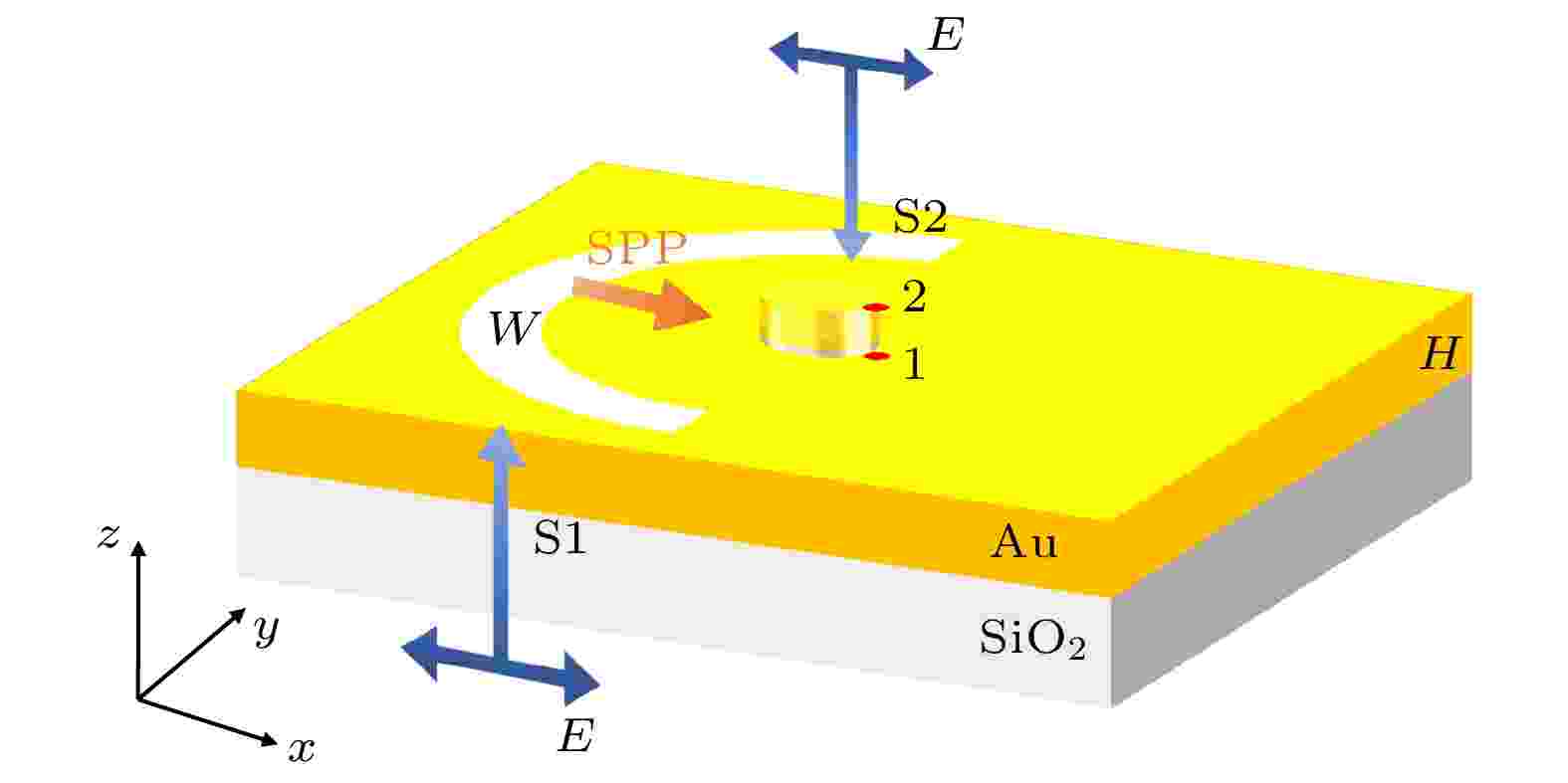
Localized surface plasmon (LSP) generated by nanostructure subjected to the excitation of surface plasmon polariton (SPP) possesses stronger near-field enhancement and special spectral and dynamic responses, thereby providing a new idea for exploring the interaction between light and matter. Meanwhile, this scheme can also release the signal background noise and structural thermal effect, and improve the performances of plasmonic components and sensing detectors based on LSP. However, the current research in this aspect is still insufficient. In this paper, we investigate the near-field characteristics of a plasmon composite structure composed of plasmon focusing lens and gold nanorod under the excitation of dual-beam by using finite-difference time-domain (FDTD) method. The result shows that the near-field intensity control on the upper surface and in the gap position of the nanorod can be achieved by adjusting the relative time delay between the first light beam (used to excite SPP) and the second light beam (used to excite LSP). Specifically, the maximum adjustment range of the near-field intensity corresponding to 770 nm resonant mode in the gap position is about 23, and the adjustment period is about 2.4 fs. In a resonant mode dominated by SPP at a wavelength of 999 nm, the adjustment range of near-field intensity is as small as 6, and the adjustment period is about 4 fs. On the upper surface of the structure, the adjustment range of the near-field intensities of the two resonant modes (719 nm and 802 nm) are basically the same (about 15), and their adjustment periods are 2.4 fs and 2.8 fs. The achievement of the near field control is attributed to the coherent superposition of SPP-excited LSP with light-excited LSP. In addition, the dephasing time of the coupling field is investigated by using a quasi- normal mode. It is found that the nanorod structure will correspond to different dephasing time under different relative time delay between two excitation light beams. Specifically, for the time delay of 0.72 fs (Δt = 0.72 fs), the corresponding dephasing times for both modes are the same (6.0 fs). For Δt = 1.92 fs, the dephasing time of the longer-wavelength mode is 7.1 fs, and the one of the shorter-wavelength mode is 5.8 fs. We attribute the difference in dephasing time to different coupling strengths between the two modes at different delay times. This study may further promote the application of plasmons in the fields of surface-enhanced Raman scattering and plasmon assisted catalysis.

EDITOR'S SUGGESTION
2023, 72 (17): 175203.
doi: 10.7498/aps.72.20230442
Abstract +
2023, 72 (17): 175204.
doi: 10.7498/aps.72.20230719
Abstract +
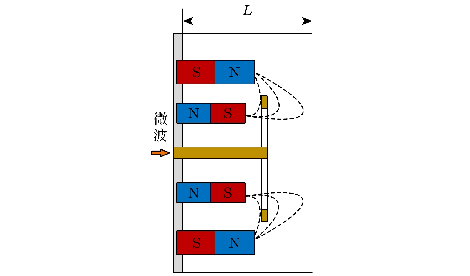
Discharge chamber length is one of the factors in optimizing the electron cyclotron resonance ion thruster performance. It adjusts the distance between bulk plasma and grid system to change the plasma density upstream of the screen grid, which will affect the ion beam current and focusing state to achieve optimization purpose. However, new evidence shows the discharge chamber length plays an important role in ionization during ion beam extraction, which means that the effect of discharge chamber length on the performance of electron cyclotron resonance ion thruster should be reexamined. After applying grid voltages, another high electron temperature region located upstream of the screen grid is observed in the integrated simulation using particle-in-cell with Monte Carlo collision method, but it is not observed in the traditional discharge chamber simulation. It is believed in the paper that the high electron temperature region exists objectively, because the Child-Langmuir sheath will repel electrons moving towards screen grid back to magnetic mirrors again. Those electrons will gain energy from microwave, and finally form a high electron temperature region along the Child-Langmuir sheath. This phenomenon implies that discharge chamber length can adjust the high electron temperature distribution upstream of screen grid to affect the plasma generation. Therefore, in this work, the effect of discharge chamber length on discharge and ion beam performance is systematically studied by adopting the integrated simulation. In this paper, three ion thrusters with different discharge chamber lengths are simulated. Under the conditions of same magnetic field and operation parameters, the comparisons of electron energy gain, plasma parameter distributions and ion beam current among the three ion thrusters are conducted. The results show that shorter discharge chamber length has higher electron energy gain, plasma density and voltage, but smaller ion beam current. This abnormal phenomenon can also be seen experimentally. By analyzing the ionization rate inside the chamber, it can be seen that high-temperature electrons upstream of the screen grid have a significant contribution to ionization. And thus, a little bit longer discharge chamber length with lower plasma density inside the chamber has bigger ion beam current for having higher plasma density upstream of the screen grid. According to this phenomenon, an electron heating mode is proposed: electrons gain energy by reciprocating through the electron cyclotron resonance layer between the Child-Langmuir sheath and magnetic mirrors. This heating mode can be used as a supplement to the electronic constraints outside the magnetic mirrors to improve the energy utilization efficiency of the thruster, which can provide a new insight into the electron cyclotron resonance ion thruster design in the future.
EDITOR'S SUGGESTION
2023, 72 (17): 175205.
doi: 10.7498/aps.72.20230854
Abstract +
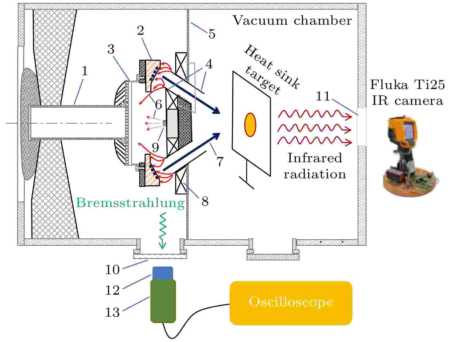
Intense pulsed ion beam (IPIB) technology has made remarkable progress in surface modification, mixing, polishing, film deposition, and nano powder synthesis in recent years. However, the surface properties of materials under IPIB irradiation are highly sensitive to beam intensity variations. Deviations from acceptable parameter range can change the surface characteristics and increase prevalence of defects. Consequently, the real-time online monitoring of beam stability during irradiation experiments and promptly identifying of pulses exhibiting significant parameter jitter are of significance in accurately analyzing results and optimizing surface modification. This study presents a fast-response pulse X-ray diagnostic system by employing EJ-200 plastic scintillator, 9266FLB photomultiplier tube, and Tektronic TDS 2024 four-channel oscilloscope. Single particle test demonstrates that the system achieves a time resolution of 6 ns, meeting the requirements for temporal response to detecting pulse X-ray signals with a half-width of ~80 ns. By adjusting the insulation magnetic field strength of the ion diode, the IPIB output level is regulated. The diagnostic system successfully captures X-rays emitted by the external magnetic insulated ion diode operating at different output levels. Simultaneously, the ion beam energy density is measured by using an infrared camera. To mitigate diagnostic errors stemming from target ablation, the maximum energy density is controlled to be below 1.32 J/cm2. Analysis results establish a positive correlation between X-ray intensity and ion beam energy density. This relationship arises from the influence of the insulating magnetic field adjustment on the diode's operating voltage, which subsequently affects the bremsstrahlung radiant intensity and ion beam emission intensity. This correlation offers the potential for the real-time monitoring of IPIB beam output stability by utilizing X-ray signals. To further corroborate the synchronized changes in pulse X-ray intensity and ion beam intensity, Faraday cup is employed as an alternative to infrared imaging method for measuring ion current density. Results demonstrate that the amplitude of the X-ray signal changes synchronously with fluctuations of ion current density. It is worth noting that when the output intensity of ion beam deviates significantly (more than 10% of the preset value), the diagnostic system will respond quickly. These findings validate the efficacy of the proposed non-interceptive diagnostic method of real-time monitoring the intense pulsed ion beam output stability.
CONDENSED MATTER: STRUCTURAL, MECHANICAL, AND THERMAL PROPERTIES
2023, 72 (17): 176401.
doi: 10.7498/aps.72.20230341
Abstract +
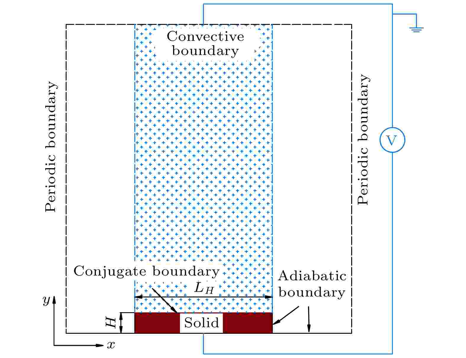
The phase change lattice Boltzmann (LB) model combined with the electric field model is employed to investigate the heat transfer performance of saturated pool boiling. Particular attention is paid to the influence of heater surface wettability and heater length on bubble behaviors, including generation, merging, and fracture during boiling in a uniform electric field. Moreover, the effects of the bubble behavior on heat transfer performance are also investigated. The study results indicate that the enhancement of boiling heat transfer by the electric field is dependent on both the heater length and the wettability. In the case of a hydrophilic surface, when the heater length $L_H^*\leqslant 6.25$ , the bubble interaction force generated on the heater surface during boiling is weak due to the small size of the heater. Thus the effect of a uniform electric field on the bubble dynamic behaviors is mainly manifested by reducing the bubble size. As a result, the whole boiling phase is suppressed in this case. In the case of $6.25 < L_H^*\leqslant9.375$ , the uniform electric field enhances the critical heat flux (CHF), and the enhancement degree increases with electric field strength increasing. This can be attributed to the longer heater providing sufficient space for bubble generation, resulting in increased bubble nucleation sites and stronger interaction forces between bubbles. On the other hand, the distance between adjacent bubbles increases with the heater length increasing,thus further contributing to the improved CHF percentage. When $L_H^*>9.375$ , the rewetting resistance increases with heater length increasing. So the vapor generated in the boiling process is prone to be closely adhered to the heating surface under the action of electric field force, forming a thin layer of vapor on the heater surface. The vapor not only increases the heat transfer thermal resistance between the solid and the fluid but also creates no vortex near the bubble. This is not conducive to the movement of the bubble to the middle of the heater, thereby slowing down the heat mass exchange between the hot fluid on the heating surface and the colder fluid on both sides. As a result, the improved percentage of CHF decreases gradually with the increase in the heater length. In the case of hydrophobic surfaces, the increased percentage of CHF initially increases with heater length increasing and then decreases. However, comparing with the hydrophilic surface, the increase of the heater source length corresponds to the beginning of the decrease of critical heat flux.

2023, 72 (17): 176801.
doi: 10.7498/aps.72.20230573
Abstract +
The superlattices composed of polar/polar perovskites have two-dimensional electron gas (2DEG) at the interface, which has broad applications in nano devices, super sensitive sensor devices, high electron mobility transistor, etc. Tuning the electronic properties of the 2DEG at the interface perovskite superlattice, such as the coupling between strain gradient and the electronic properties of the 2DEG in correlated electronic systems, is of great significance. In this paper, the properties of (LaAlO3)4.5/(KNbO3)8.5 superlattice, which is composed of KNbO3 and LaAlO3, are systematically investigated through first-principles density functional theory calculations. The band structure of (LaAlO3)4.5/(KNbO3)8.5 superlattice exhibits 2DEG at the interface, which is consistent with the result in the literature. The band structure, density of states, magnetic moments and carrier concentration at the interface are fully investigated by using compressive gradient and tensile strain gradient, respectively. The results show that compressive strain gradient can effectively reduce the 2DEG concentration at the interface. When the compressive strain gradient coefficient reaches 12%, the 2DEG concentration decreases by 76.4%, and the interface magnetic moment disappears. The total magnetic moment of the superlattice decreases by 88.44%. When the tensile strain gradient is 12%, the electron gas concentration at the interface is increased by about 23.9%, and the interface magnetic moment is reduced by about 90.7%. At the same time, an obvious magnetic moment appears in the layer near the interface. Hence, the strain gradient can be a new approach to regulating the electron gas concentration at interface of perovskite superlattice. The tensile strain gradient increases the electron gas concentration at the interface, while the compressive strain gradient reduces the electron gas concentration. Therefore, it opens up a new way to exploring the regulation of high-performance spin polarized carrier gas at the oxide interface.
CONDENSED MATTER: ELECTRONIC STRUCTURE, ELECTRICAL, MAGNETIC, AND OPTICAL PROPERTIES

EDITOR'S SUGGESTION
2023, 72 (17): 177102.
doi: 10.7498/aps.72.20230621
Abstract +
Co3Sn2S2 is a magnetic Weyl semimetal with special magnetic and electronic structure. Its unique band structure makes it have many interesting physical properties such as abnormal Hall effect, negative magnetoresistance effect, and abnormal Nernst effect. In this work, high quality Co3Sn2S2 single crystal with a dimension of 8 mm×7 mm×0.5 mm is synthesized by self-flux method. We measure its electrical transport properties (magnetoresistance effect, Hall effect, etc.) and thermal transport properties (Seebeck effect) at low temperature. The free surface of the single crystal exhibits obvious layered growth characteristics, indicating that the Co3Sn2S2 crystal grows along the c-axis direction. The value of the normalized resistivity ρ3 K/ρ300 K for the single crystal sample at 3 K is only 0.08, indicating that the crystal quality of the sample is at a relatively high level. The thermomagnetic (M-T) curves show that a special magnetic structure near 140 K (TA) below the Curie temperature point (TC = 178 K). This special magnetic structure is a magnetic transition state in which ferromagnetic state and antiferromagnetic state coexist, making them appear as a local minimum point in the M-T curve. The Co3Sn2S2 shows a negative anomalous “convex” magnetoresistance in a large range of 100—160 K, and there exists a maximum critical magnetic field B0 (1.41 T), near TA. The coercivity HC drops to almost zero at TA and the Hall resistivity ρyx also reaches a maximum value of about 20 μΩ·cm. This may be due to the competition between ferromagnetic state and antiferromagnetic state to form non-trivial spin texture, resulting in the unique electrical transport behavior near TA. When the temperature rises to TC, the Co3Sn2S2 undergoes a ferromagnetic phase transition, with a saturation magnetization of MS, anomalous Hall conductivity $ {\sigma }_{yx}^{\rm A} $ , and Hall resistivity ρyx sharply decreasing. Large anomalous Hall conductance $ {\sigma }_{yx}^{A} $ and anomalous Hall angle $ {\sigma }_{yx}^{\rm A}/\sigma $ are also present in Co3Sn2S2, with these values reaching 1.4×10³ Ω−1·cm−1 and 18%, respectively. The magnetoresistance measurements reveal that the variation of the magnetoresistance with the magnetic field is due to the combination of linear and parabolic contributions. The change in magnetoresistance with the angle θ between the magnetic field B and the current I has a reversal symmetry with C2x symmetry, and the change in θ does not affect the contribution of its magnetoresistance source. In addition, positive magnetoresistance and negative magnetoresistance are found to be shifted at about 60 K. the shift in positive magnetoresistance and negative magnetoresistance are mainly attributed to the competing positive contribution of the Lorentz force to the magnetoresistance and the negative contribution of the spin disorder. The scattering mechanism of Co3Sn2S2 at low temperature is a combination of acoustic wave scattering and electron– phonon scattering. At 60–140 K, the enhancement of spin disorder causes enhanced electron–phonon scattering, resulting in a plateau characteristic of the Seebeck coefficient S. The research shows that the special magnetic structure and electron spin of Co3Sn2S2 at low temperatures have an important influence on its electrothermal transport behavior.
EDITOR'S SUGGESTION
2023, 72 (17): 177201.
doi: 10.7498/aps.72.20230949
Abstract +
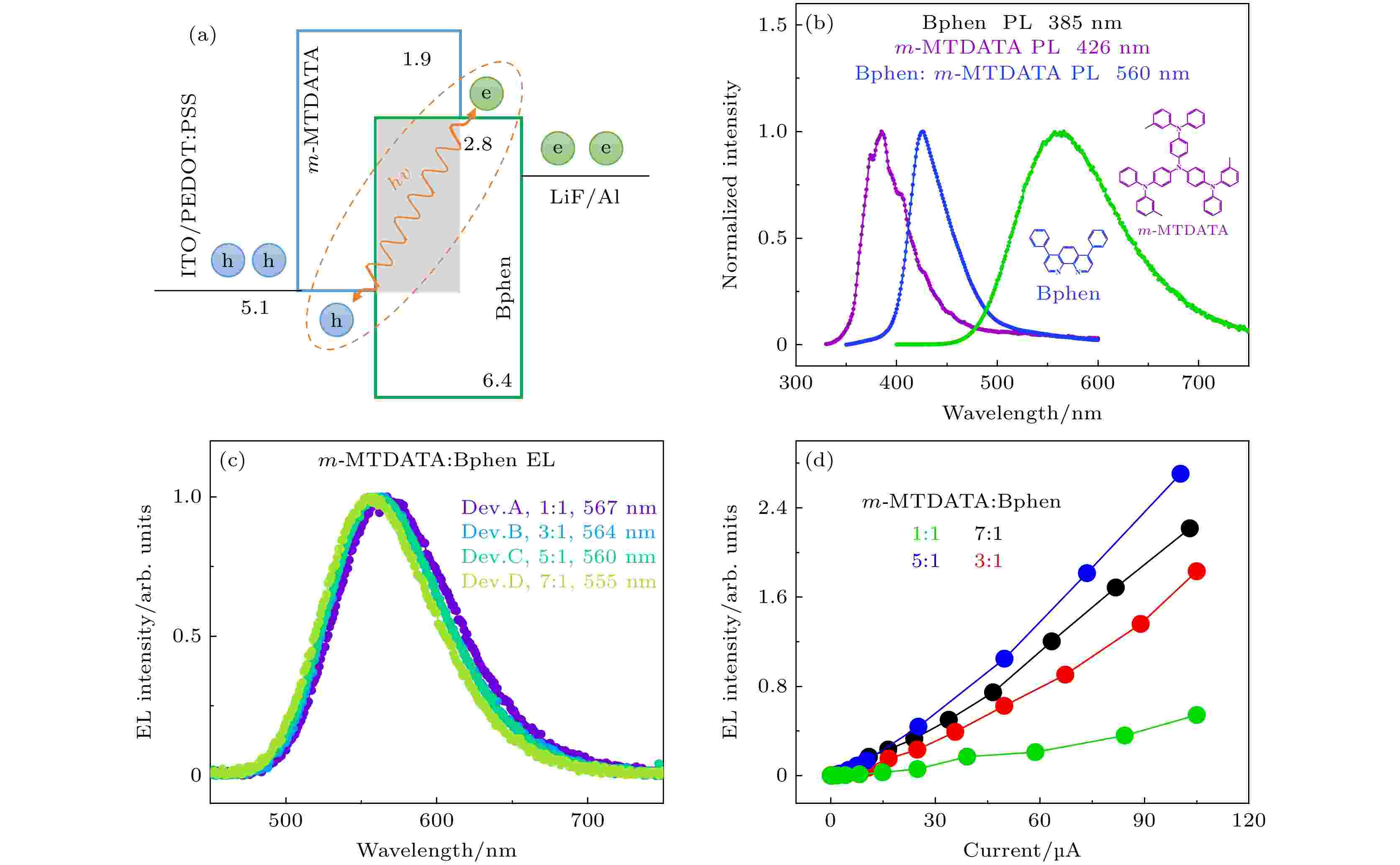
The reverse inter-system crossing (RISC, CT3 → CT1) process in charge transfer (CT1 and CT3) states is an effective approach to improving the energy utilization rate of excited states, and precise control and full use of the RISC process have important scientific significance and application prospect for fabricating and realizing the efficient exciplex-type organic light-emitting diodes (OLEDs). The conventional exciplex-type OLEDs based on m-MTDATA: Bphen have received extensive attention among researchers owing to the fact that the energy difference between CT1 and CT3 around zero promotes the efficient occurrence of RISC process. But up to now, only transient photoluminescence can infer the existence of RISC process in experiment, which is quite unfavorable for the comprehensive understanding and application of this process to design high-performance OLEDs. Fortunately, in this paper, a series of balanced and unbalanced exciplex-based devices are prepared by changing the donor-acceptor blending ratio in the emitting layer (x% m-MTDATA:y% Bphen; x%, y% is the weight percent) and the carrier density flowing through the device. The RISC process of CT states is directly observed via analyzing fingerprint magneto-conductance (MC) traces of the balanced device at room temperature, and the balanced device has higher electroluminescence (EL) efficiency than the unbalanced device. Specifically, the low-field MC curves of unbalanced device only show an inter-system crossing (ISC) line shape, whereas those from the balanced exciplex device present an RISC line shape at low bias-current and the conversion into an ISC line shape with the further increase of bias current. The line shape transition from RISC to ISC is attributed to the triplet-charge annihilation (TQA) process caused by excessive charge carries under high bias current. Combining the physical microscopic mechanism of device, the above-mentioned MC curves of various exciplex devices can be explained as follows: under the same bias current, extra holes or electrons are generated in the emitter layer of unbalanced devices due to the mismatch of donor-acceptor molecular concentrations. These superfluous holes or electrons will react with the CT3 state, which aggravates the TQA process in the device and weakens the RISC process in which the CT3 state participates. That is to say, there are strong TQA process and weak RISC process in unbalanced exciplex device. Contrarily, the strong RISC process and weak TQA process in the balanced exciplex device are beneficial to the occurrence of delayed fluorescence, resulting in its EL efficiency higher than that of the unbalanced device. This work not only deepens the physical understanding of the influence of donor-acceptor blending ratio on the carrier balance in exciplex devices, but also paves the way for designing highly efficient OLED by fully employing the RISC process of balanced device.

2023, 72 (17): 177701.
doi: 10.7498/aps.72.20230664
Abstract +
The electro-optical properties of polymer dispersed liquid crystal film vary with liquid crystal content and externally applied electric field, but the analysis of the film morphology cannot directly reflect the mechanism of electro-optical properties. Therefore, the polymer dispersed liquid crystal film prepared by blending liquid crystal material E7 and photopolymer NOA65 is used. Herein, the dielectric polarization regulated electro-optical properties and their related mechanisms under different liquid crystal content and electric fields are revealed. The results show that in a frequency range of 10–1–106 Hz, the film exhibits three relaxation processes respectively at low frequency, medium frequency and high frequency, which are generated by thermionic polarization, interfacial polarization and orientation polarization. According to the Arrhenius equation, the activation energy values of such polarization processes are calculated. It is found that with the increase of liquid crystal content, the activation energy of orientation polarization decreases from 0.88 eV to 0.83 eV, leading the threshold field strength and the saturation field strength of the diversion of liquid crystal molecule to decrease. Thermionic polarization under DC electric field forms an internal electric field, which causes the threshold field strength and saturation field strength to increase greatly, as compared with the scenarios under AC electric field. Such a thermionic polarization also leads the polarization relaxation time to increase, resulting in the extension of response time. This study is of guiding significance in further analyzing and improving the electro-optical properties of polymer dispersed liquid crystal films.
2023, 72 (17): 177801.
doi: 10.7498/aps.72.20230685
Abstract +
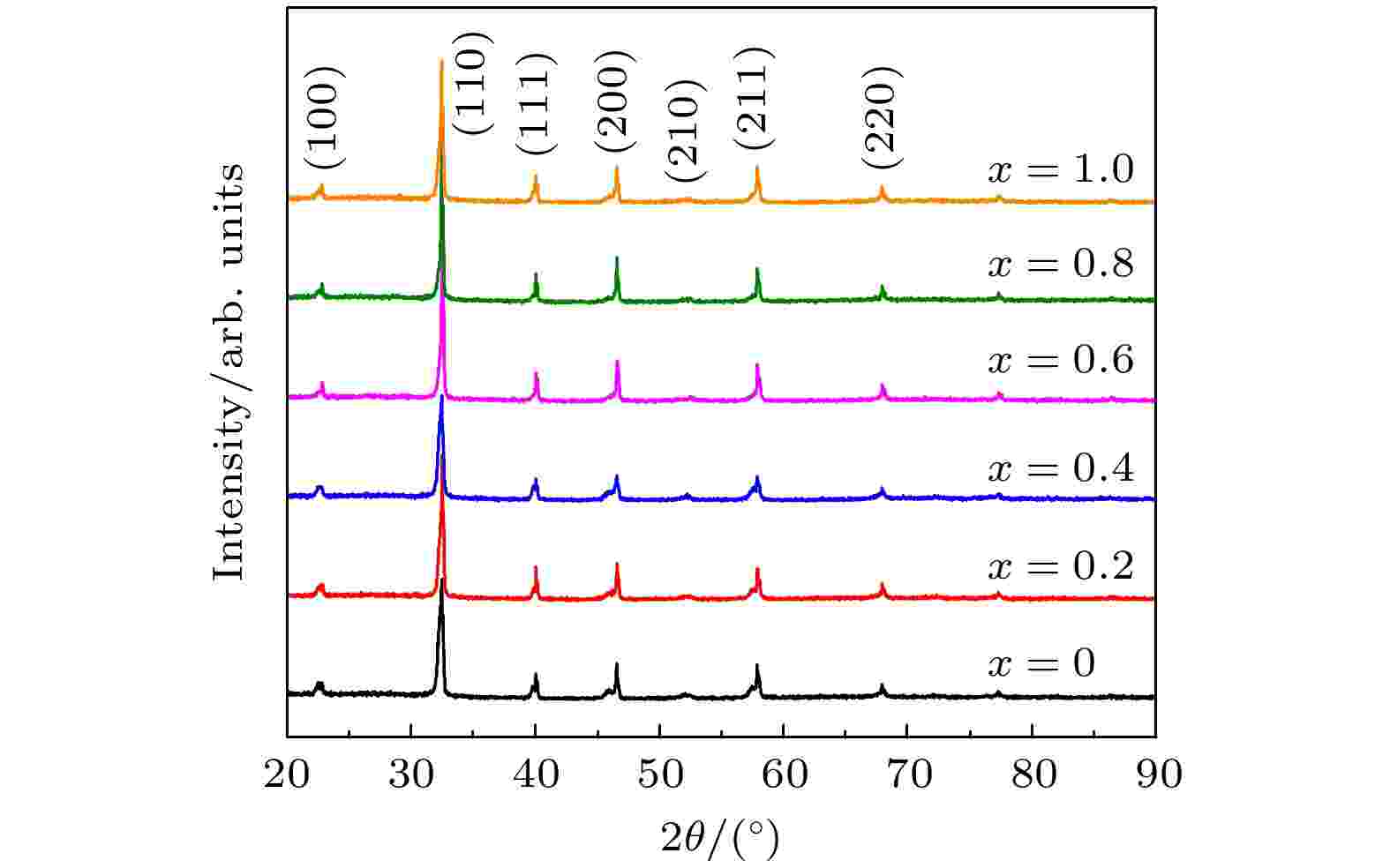
In recent years, inorganic multifunctional ferroelectric ceramics have been widely utilized in various fields, including aerospace, optical communication, and capacitors, owing to their high stability, easy synthesis, and flexibility. Rare-earth doped ferroelectric materials hold immense potential as a new type of inorganic multifunctional material. This work focuses on the synthesis of x%Sm3+-doped 0.94Bi0.5Na0.5TiO3-0.06BaTiO3 (BNTBT:x%Sm3+ in short) ceramics by using the conventional solid-state sintering method, aiming to comprehensively investigate their ferroelectric, energy storage, and photoluminescence (PL) properties. The X-ray diffraction analysis reveals that the introduction of Sm3+ does not trigger off the appearing of secondary phases or changing of the original perovskite structure. The scanning electron microscope (SEM) images demonstrate that Sm3+ incorporation effectively restrains the grain growth in BNTBT, resulting in the average grain size decreasing from 1.16 to 0.95 μm. The reduction in remanent polarization (Pr) and coercive field (Ec) can be attributed to both the grain size refinement and the formation of morphotropic phase boundaries (MPBs). Under an applied field of 60 kV/cm, the maximum value of energy storage density (Wrec) reaches to 0.27 J/cm3 at an Sm3+ doping concentration of 0.6%. The energy storage efficiency (η) gradually declines with electric field increasing and stabilizes at approximately 45% for Sm3+ doping concentrations exceeding 0.6%. This result can be ascribed to the decrease in ΔP (Pmax – Pr) due to the growth of ferroelectric domains as the electric field increases. Additionally, all Sm3+-doped BNTBT ceramics exhibit outstanding PL performance upon being excited with near-ultraviolet (NUV) light at 408 nm, without peak position shifting. The PL intensity peaks when the Sm3+ doping concentration is 1.0%, with a relative change (ΔI/I) reaching to 700% at 701 nm (4G5/2→6H11/2). However, the relative change in PL intensity is minimum at 562 nm (4G5/2→6H5/2) due to the fact that the 4G5/2→6H5/2 transition represents a magnetic dipole transition, and the PL intensity remains relatively stable despite variations in the crystal field environment surrounding Sm3+. Our successful synthesis of this novel ceramic material, endowed with both energy storage and PL properties, offers a promising avenue for developing inorganic multifunctional materials. The Sm3+-doped BNTBT ceramics hold considerable potential applications in optical memory and multifunctional capacitors.
2023, 72 (17): 177802.
doi: 10.7498/aps.72.20230855
Abstract +
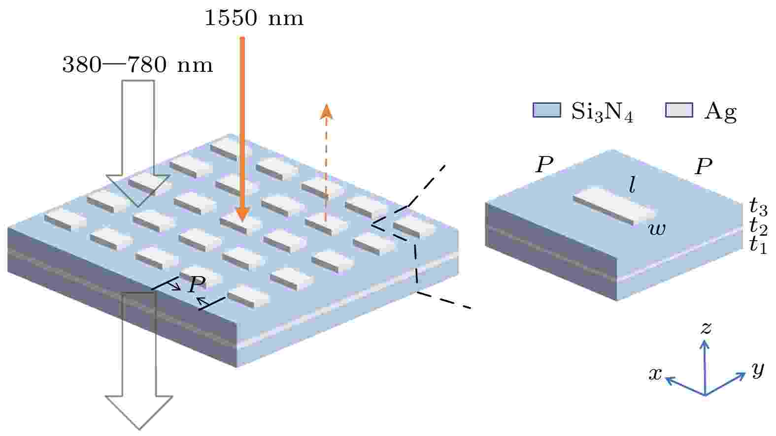
The “cat’s eye effect” in the optical window of all kinds of photoelectric equipment is the main basis of a laser active detection system, which poses a great threat to military equipment and combatants. However, under the condition of ensuring high visible transmittance, the sniper stealth scheme for anti-laser active detection remains to be discussed. In this paper, genetic algorithm is used to inverse design the metasurface anti-reflection film. The three-layer anti-reflection film are composed of Si3N4 and Ag , and rectangular array of metal micro-nano structures is added on the top layer to form a wavelength selective absorber, so as to achieve the effect of low reflection and high absorption at laser wavelength. By combining the device design with genetic algorithm, the parameter combination that best possesses the target performance of the device is obtained. The average transmittance in a wavelength range of 380–780 nm is 88%, and a maximum transmittance peak is 94%. The reflectance and the absorption rate at 1550 nm are achieved to be 10% and 80%, respectively. In order to better meet the requirements for practical application, we further design the cross metal array to obtain polarization insensitive characteristics. The metasurface anti-reflective membrane with improved structure can achieve an average visible transmittance of 82% and a reflectance of 5% at 1550 nm. The two metasurface anti-reflection films designed in this work do not require additional devices, and the imaging quality can be guaranteed. At the same time, it can effectively reduce the laser echo energy, so as to achieve the effect of high-quality visible light transmittance and laser stealth compatibility.
INTERDISCIPLINARY PHYSICS AND RELATED AREAS OF SCIENCE AND TECHNOLOGY
2023, 72 (17): 178101.
doi: 10.7498/aps.72.20230711
Abstract +
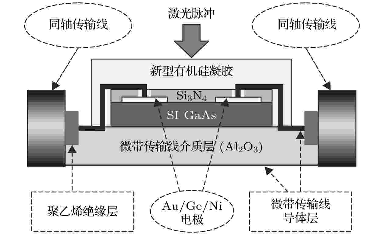
Photoconductive semiconductor switch is of significance in the fields of ultafast electronics, high-repetition rate and high-power pulse power system, and THz radiation. The mechanism of the nonlinear mode of the switch is an important area of study. In this work, stable nonlinear wave forms are obtained by a semi-insulating GaAs photoconductive semiconductor switch triggered by a 5-ns laser pulse with pulsed energy of 1 mJ at a wavelength of 1064 nm under a bias of 2750 V. Based on two-photon absorption model, the photogenerated carrier concentration is calculated. The theory analysis and calculation result show that the photogenerated carrier can compensate for the lack of intrinsic carrier, and lead to the nucleation of photo-activated charge domain. According to transferred-electron effect principium, the electric field inside and outside the domain are calculated, indicating that the electric field within the domain can reach the electric field which is much larger than intrinsic breakdown electric field of GaAs material, and results in strong impact avalanche ionization in the bulk of the GaAs switch. According to the avalanche space charge domain, the typical experimental phenomena of nonlinear mode for GaAs switch are analyzed and calculated, the analysis and calculations are in excellent agreement with the experimental results. Based on drift-diffusion model and negative differential conductivity effect, the transient electric field in the bulk of the switch is simulated numerically under the optical triggering condition. The simulation results show that there are moving multiple charge domains with a peak electric filed as high as the intrinsic breakdown electric field of GaAs within the switch. This work provides the experimental evidence and theoretical support for studying the generation mechanism of the nonlinear photoconductive semiconductor switch and the improvement of the photo-activated charge domain theory.
EDITOR'S SUGGESTION
2023, 72 (17): 178401.
doi: 10.7498/aps.72.20230693
Abstract +
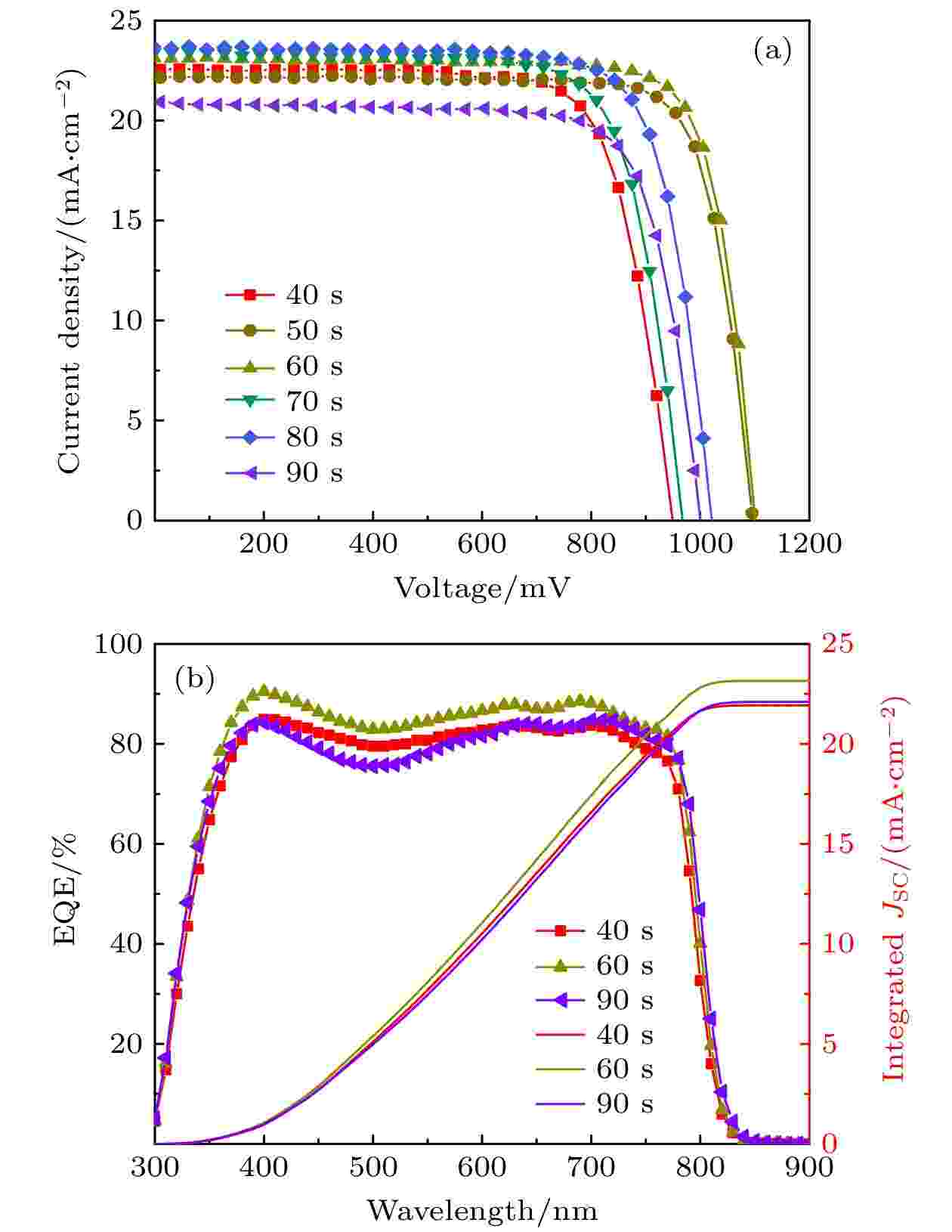
The electron transport layer is very important for the device efficiency and stability of perovskite solar cells. Tin dioxide is a common electron transport layer in high-efficiency solar cells and has good carrier extraction and transport capability. However, using the solution method to prepare tin dioxide, a large number of defects are generated on its surface during high-temperature annealing in air, which can degrade the electrical properties of the film, so the solution method is not conducive to preparing large-area film. In this paper, the reactive plasma deposition method is used to prepare tin dioxide thin film, and the performance of the thin film is optimized by adjusting the glow discharge time and working current. The film is applied to small-area N-I-P type perovskite solar cells, the efficiency reaching to 21.24%. The hysteresis of the device is improved by introducing stannous isooctanoate and tin dioxide as a double electron transport layer, the open circuit voltage of the solar cell increases from 1.11 to 1.15 V, the efficiency rises from 21.27% to 22.15%, and the hysteresis factor decreases from 24.04% to 3.69%. This work presents a new preparation method and effective optimization strategy to prepare tin dioxide electron transport layer, which will promote the development of planar heterojunction perovskite solar cells and provide a new research idea for preparing high-efficiency and stable perovskite solar cells.
2023, 72 (17): 178501.
doi: 10.7498/aps.72.20230709
Abstract +
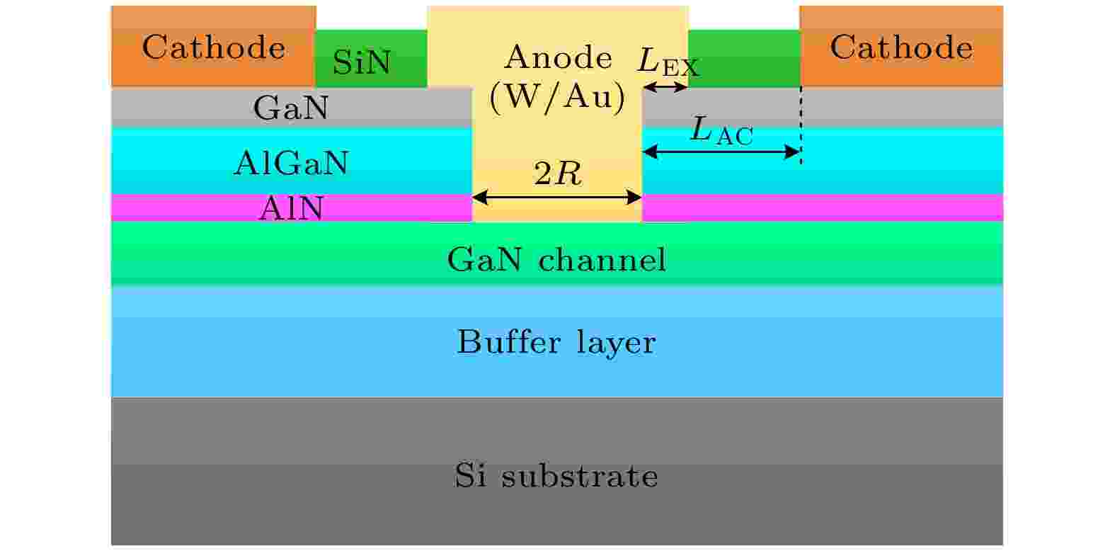
AlGaN/GaN heterojunction epitaxies with wide bandgap, high critical electric field as well as high density and high mobility two-dimensional electron gas have shown great potential applications in the next-generation high-power and high-frequency devices. Especially, with the development of Si-based GaN epitaxial technique with big size, GaN devices with low cost also show great advantage in consumer electronics. In order to improve the rectification efficiency of AlGaN/GaN Schottky barrier diode (SBD), low leakage current and low turn-on voltage are important. The GaN Schottky barrier diode with low work-function metal as anode is found to be very effective to reduce turn-on voltage. However, the low Schottky barrier height makes the Schottky interface sensitive to damage to groove surface, which leads to a high leakage current. In this work, a novel wet-etching technique with thermal oxygen oxidation and KOH corrosion is used to prepare the anode groove, and the surface roughness of groove decreases from 0.57 to 0.23 nm, compared with that of the dry-etching surface of groove. Meanwhile, the leakage current is suppressed from 1.5 × 10⁻⁶ to 2.6 × 10⁻⁷ A/mm. Benefiting from the great corrosion selectively of hot KOH solution to AlGaN barrier layer and GaN channel layer after thermal oxygen oxidation, the spikes of the edge of groove region caused by the nonuniform distribution of plasma in the cavity is improved, and the breakdown voltage of the fabricated AlGaN/GaN SBDs is raised from –1.28 to –1.73 kV.
2023, 72 (17): 178801.
doi: 10.7498/aps.72.20230292
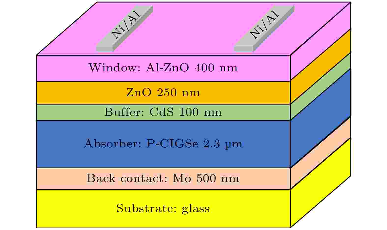
Abstract +
We use admittance spectroscopy to characterize the energy distribution of defects in CIGSe solar cells before and after annealing to investigate the mechanism of the annealing process improving the performances of solar cells. In this work, we anneal the prepared CIGSe solar cells in compressed air at 150 ℃ for 10 min. We measure dark I-V, C-V, admittance spectra, and illumination I-V tests on CIGSe solar cells before and after annealing to characterize the changes in the performances of solar cells before and after annealing, respectively. The test results of dark I-V characteristics show that the reverse dark current of CIGSe solar cell decreases by about an order of magnitude after annealing, and the ideal factor of the cell also decreases from 2.16 (before annealing) to 1.85 (after annealing). This means that the annealing process reduces the recombination of carriers in CIGSe solar cell. Under reverse bias, the capacitance of CIGSe solar cell is higher than that after annealing, and its C-V characteristics linearly fitted with 1/C 2 vs. V. The fitting results show that the slope of the curve increases after annealing, which means that the annealing process results in a decrease in the free carrier concentration in the absorption layer of CIGSe solar cell, specifically, the carrier concentration contributed by defects after annealing decreases. In addition, the built-in potential before and after annealing of CIGSe solar cell are also obtained through fitting, which are 0.52 V and 0.64 V in value, respectively. The admittance spectrum test results of CIGSe solar cell before and after annealing show that the defect activation energy in the absorption layer significantly decreases after annealing, but the defect concentration remains almost unchanged. The decrease in defect activation energy means that the Shockley Read Hall (SRH) recombination probability of defects in copper indium gallium selenium solar cell decreases. In addition, the test results of the optical I-V characteristics of the battery indicate that the open circuit voltage and parallel resistance of the solar cell significantly increase after annealing, which is consistent with the test results of the dark I-V characteristics, C-V characteristics, and admittance spectroscopy of the solar cell. Therefore, the annealing process of CIGSe solar cells leads to theweakening of the SRH recombination of carriers in the absorption layer of the cell, thereby improving the performance of the solar cell.


