-
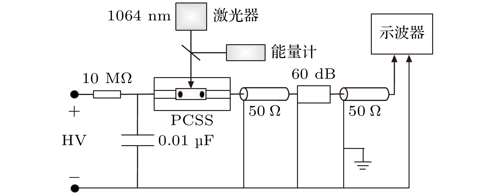
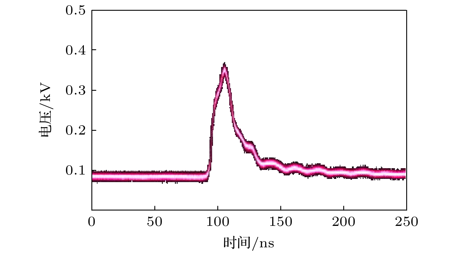
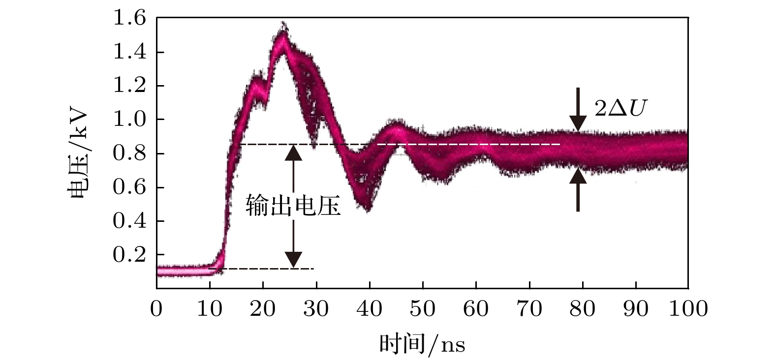
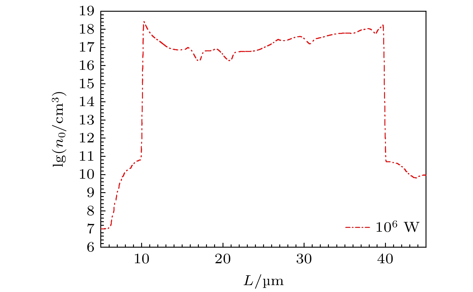
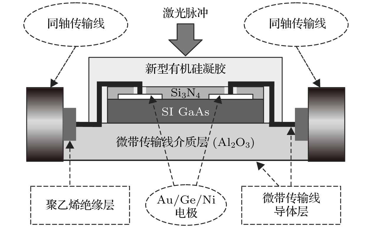
Photoconductive semiconductor switch is of significance in the fields of ultafast electronics, high-repetition rate and high-power pulse power system, and THz radiation. The mechanism of the nonlinear mode of the switch is an important area of study. In this work, stable nonlinear wave forms are obtained by a semi-insulating GaAs photoconductive semiconductor switch triggered by a 5-ns laser pulse with pulsed energy of 1 mJ at a wavelength of 1064 nm under a bias of 2750 V. Based on two-photon absorption model, the photogenerated carrier concentration is calculated. The theory analysis and calculation result show that the photogenerated carrier can compensate for the lack of intrinsic carrier, and lead to the nucleation of photo-activated charge domain. According to transferred-electron effect principium, the electric field inside and outside the domain are calculated, indicating that the electric field within the domain can reach the electric field which is much larger than intrinsic breakdown electric field of GaAs material, and results in strong impact avalanche ionization in the bulk of the GaAs switch. According to the avalanche space charge domain, the typical experimental phenomena of nonlinear mode for GaAs switch are analyzed and calculated, the analysis and calculations are in excellent agreement with the experimental results. Based on drift-diffusion model and negative differential conductivity effect, the transient electric field in the bulk of the switch is simulated numerically under the optical triggering condition. The simulation results show that there are moving multiple charge domains with a peak electric filed as high as the intrinsic breakdown electric field of GaAs within the switch. This work provides the experimental evidence and theoretical support for studying the generation mechanism of the nonlinear photoconductive semiconductor switch and the improvement of the photo-activated charge domain theory.
-
Keywords:
- GaAs photoconductive semiconductor switches /
- nonlinear mode /
- two-photon absorption /
- photoactivated avalanche charge domain
[1] Sun G X, Wang X, Ding W D, Yan J Q, Shen S K, and Nie S H 2023 IEEE Trans. Electron Dev. 70 765
 Google Scholar
[2] Shi W, Tian L Q, Liu Z, Zhang L Q, Zhang Z Z, Zhou L J, Liu H W, Xie W P 2008 Appl. Phys. Lett. 92 043511
 Google Scholar
[3] Han K H, Zhao W J, Zeng X, Chu E Y, Jiao Q J 2023 IEEE T. Power Electron. 38 3375
 Google Scholar
[4] Loubriel G M, Zutavern F J, Baca A G, Hjalmarson H P, Plut T A, Helgeson W D, O’Malley M W, Ruebush M H, and Brown D J 1997 IEEE T. Plasma Sci. 25 124
 Google Scholar
[5] Zhang D H, Xu Z, Cheng G, Liu Z, Gutierrez A R, Zang W, Norris T B, Zhong Z H 2022 Nat. Commun. 13 6404
 Google Scholar
[6] Lu P K, Jiang X H, Zhao Y F, Turan D, Jarrahi M 2022 Appl. Phys. Lett. 120 261107
 Google Scholar
[7] Woo K, Malakoutian M, Reeves B A, Chowdhury S 2022 Appl. Phys. Lett. 120 112104
 Google Scholar
[8] 桂淮濛, 施卫 2019 物理学报 68 194206
 Google Scholar
Gui H M, Shi W 2019 Acta Phys. Sin. 68 194206
 Google Scholar
[9] Tian L Q, Shi W, Feng Q Q 2011 J. Appl. Phys. 110 094507
 Google Scholar
[10] 施卫, 田立强, 王馨梅, 徐鸣, 马德明, 周良骥, 刘宏伟, 谢卫平 2009 物理学报 58 1219
 Google Scholar
Shi W, Tian L Q, Wang X M, Xu M, Ma D M, Zhou L J, Liu H W, Xie W P 2009 Acta Phys. Sin. 58 1219
 Google Scholar
[11] Zutavern F J, Glover S F, Reed K W, Cich M J, Mar A, Swalby M E, Saiz T A, Horry M L, Gruner F R, White F E 2008 IEEE T. Plasma Sci. 36 2533
 Google Scholar
[12] Kelkar K S, Islam N E, Fessler C M, Nunnally W C 2006 J. Appl. Phys. 100 124905
 Google Scholar
[13] Liu R J, Shang A N, Chen C J, Lee Y G, Yin S Z 2021 Opt. Lett. 46 825
 Google Scholar
[14] 王志权, 施卫 2022 物理学报 71 188704
Wang Z Q and Shi W 2022 Acta Phys. Sin. 71 188704
[15] 施卫, 马湘蓉, 薛红 2010 物理学报 59 5700
 Google Scholar
Shi W, Ma X R, Xue H 2010 Acta Phys. Sin. 59 5700
 Google Scholar
[16] Kelkar K, Islam N E, Kirawanich P, Fessler C M, Nunnally W C, Kemp W T, Sharma A K 2007 IEEE T. Plasma Sci. 35 93
 Google Scholar
[17] Chao J H, Zhu W B, Chen C J, Lee Y G, Shang A N, Yin S Z, Hoffman R C 2018 Opt. Lett. 43 3929
 Google Scholar
[18] Hu L, Su J C, Qiu R C, Fang X 2018 IEEE T. Electron Dev. 65 1308
 Google Scholar
[19] Chowdhury A R, Dickens J C, Neuber A A, Ness R, Joshi R P 2018 J. Appl. Phys. 123 085703
 Google Scholar
[20] 施卫, 薛红, 马湘蓉 2009 物理学报 58 8554
 Google Scholar
Shi W, Xue H, Ma X R 2009 Acta Phys. Sin. 58 8554
 Google Scholar
[21] Sun Y, Hu L, Li Y D, Zhu L, Dang X, Hao Q S, Li X 2022 J. Phys. D Appl. Phys. 55 215103
 Google Scholar
[22] Shi W, Tian L Q 2006 Appl. Phys. Lett. 89 202103
 Google Scholar
[23] Bosch B G, Engelmann R W H 1975 Gunn-Effect Electrics (Pitman: Bath) p23
[24] Kroemer H 1965 Proc. IEEE 53 1246
 Google Scholar
[25] Sze S M 1981 Physics of Semiconductor Devices (2nd Ed.) (New York: Wiley & Sons) p652
[26] Liu X H, Shi B, Jia G, Chen Z G, Ren C, Zhang Y H, Cao K, Zhao J X 2007 Appl. Phys. Lett. 90 101109
 Google Scholar
[27] Garcia H, Kalyanaraman R 2007 Appl. Phys. Lett. 91 111114
 Google Scholar
[28] Montoya J, Hu Q 2004 J. Appl. Phys. 95 2230
 Google Scholar
[29] Islam N E, Schamiloglu E, Fleddermann C B, Schoenberg J S H, Joshi R P 1999 J. Appl. Phys. 86 1754
 Google Scholar
[30] Gunn J B 1967 IEEE Trans. Electron Devices ED-14 720
[31] Copeland J A 1966 J. Appl. Phys. 37 3602
 Google Scholar
[32] Vainshtein S, Yuferev V, Palankovski V, Ong D S, Kostamovaara J 2008 Appl. Phys. Lett. 92 062114
 Google Scholar
[33] Zhao H M, Hadizad P, Hur J H, Gundersen M A 1993 J. Appl. Phys. 73 1807
 Google Scholar
[34] Vainshtein S, Kostamovaara J, Sveshnikov Y, Gurevich S, Kulagina M, Yuferev V, Shestak L, Sverdlov M 2004 Electron. Lett. 40 85
 Google Scholar
[35] Zutavern F, Loubriel G, McLaughlin D, Helgeson W, O’Malley M 1992 Proc. SPIE 1632 152
 Google Scholar
[36] Zutavern F J, Loubriel G M, O'Malley M W, Helgeson W D, Mclaughlin D L 1991 Proceedings of the Eighth IEEE International Conference on Pulsed Power San Diego, CA, USA, June 16–19, 1991 p23
[37] Tian L Q, Wang H Q, Jing D, Pan C, Shi W, Zhang C 2021 IEEE Trans. Electron Devices 68 2189
 Google Scholar
-
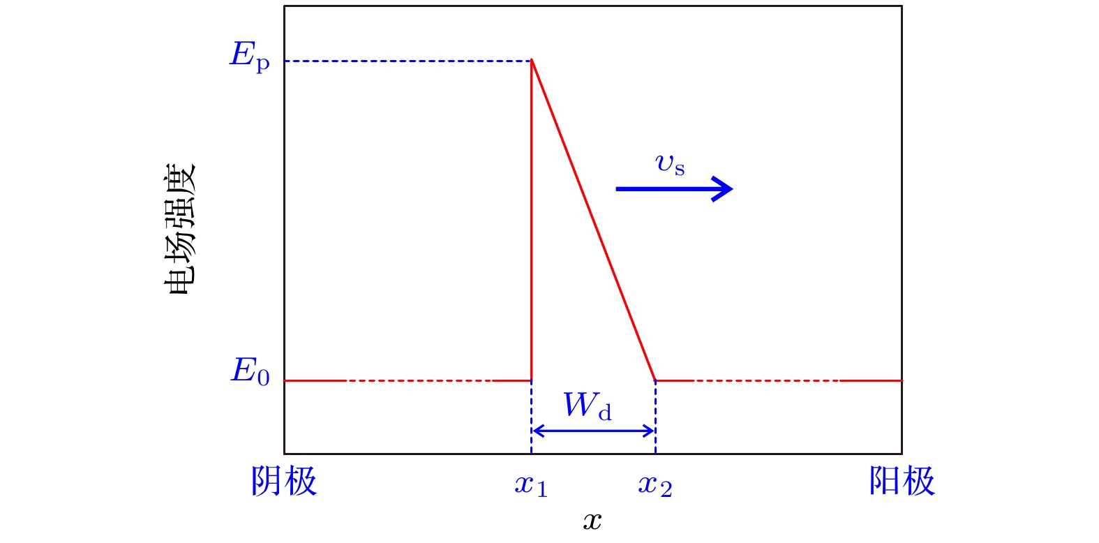
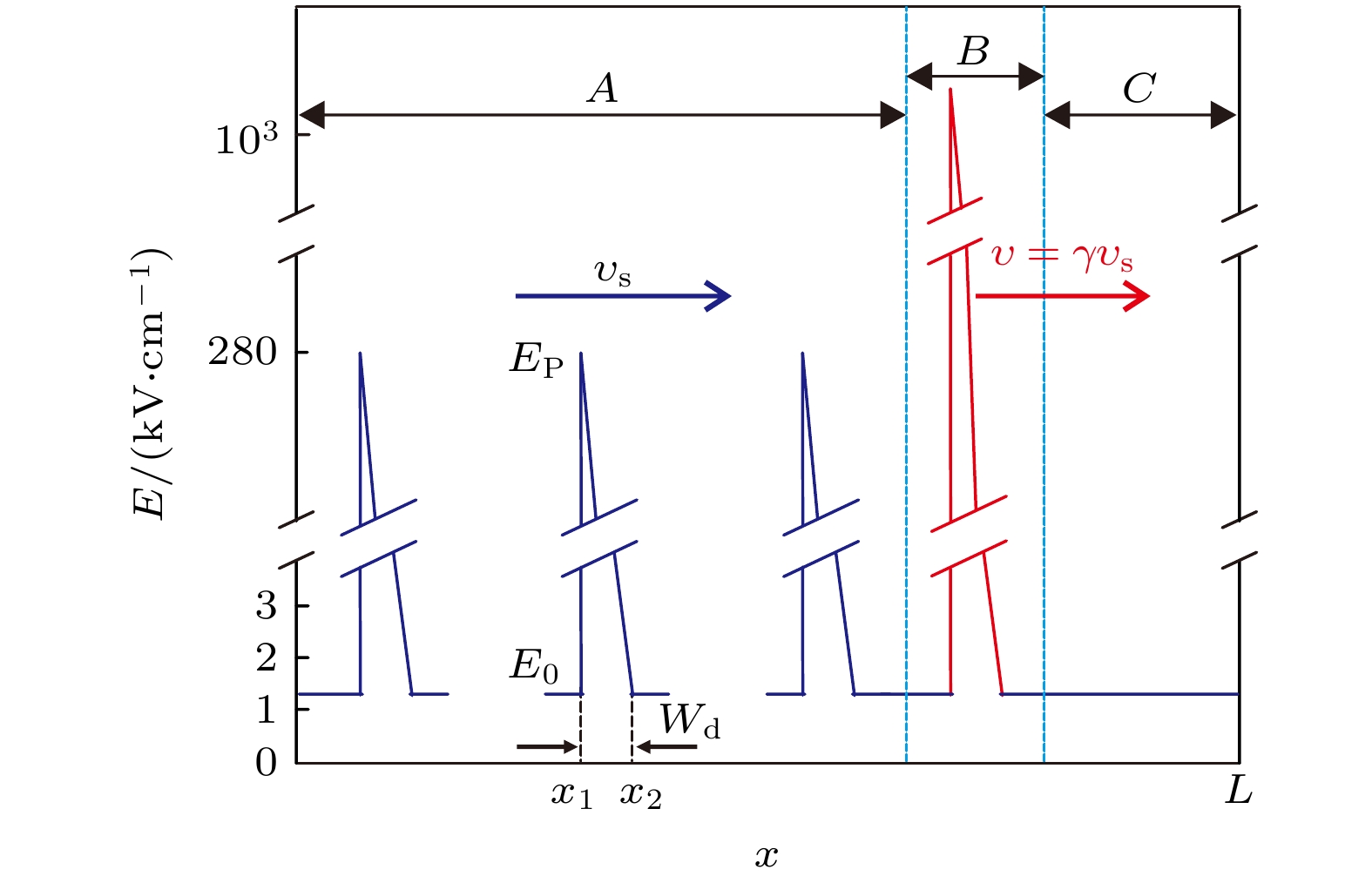
图 5 电场呈三角形分布的空间电荷畴的示意图, Ep为畴内峰值电场, E0为畴外电场, Wd为畴宽, υs为载流子饱和漂移速度, x1和x2分别为电荷畴后端和前端位置坐标
Figure 5. Schematic of the space charge domains with a triangular shape electric field distribution, Ep is the peak electric field within the domain, E0 denotes the external electric field of the domain, and υs indicates the saturation drift velocity of the carriers, x1 and x2 represent the posterior and anterior position coordinates of the charge domain, respectively.
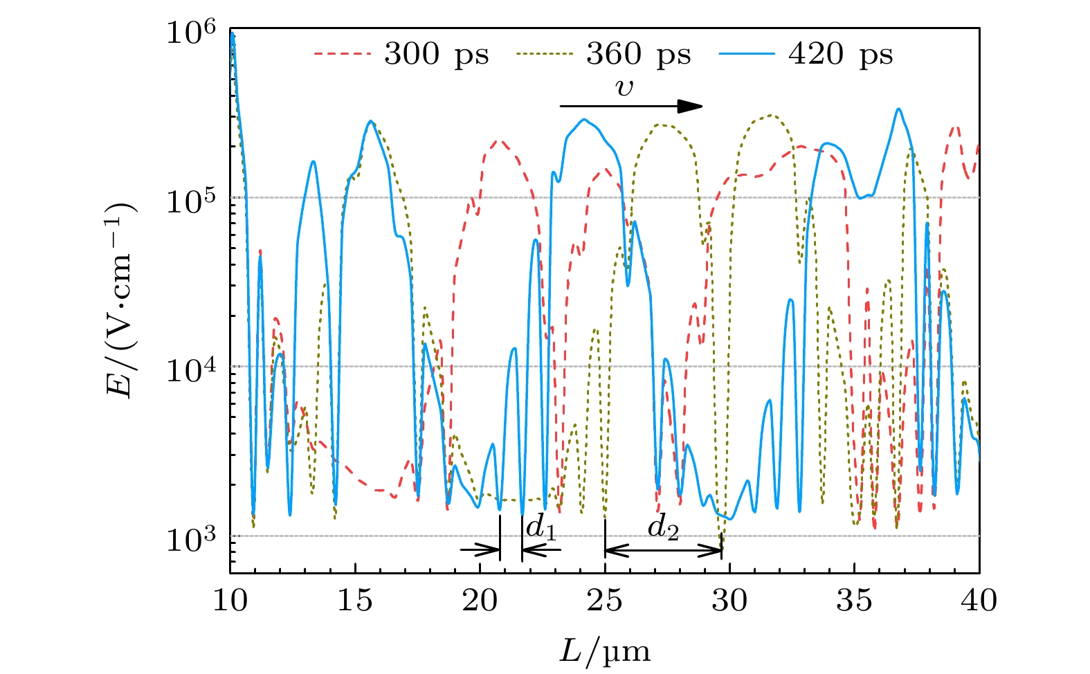
图 8 器件触发后300, 360和420 ps时开关体内瞬变电场分布, d1和d2分别子畴和主畴的宽度, υ为电荷畴的漂移速度
Figure 8. Snapshots of the electric field profiles in the bulk of the switch at 300, 360 and 420 ps, respectively after the switch triggered by the light. Here, d1 and d2 denote the width of subsidiary charge domain and main charge domain, repectively, and υ is drift velocity of the charge domain.
-
[1] Sun G X, Wang X, Ding W D, Yan J Q, Shen S K, and Nie S H 2023 IEEE Trans. Electron Dev. 70 765
 Google Scholar
[2] Shi W, Tian L Q, Liu Z, Zhang L Q, Zhang Z Z, Zhou L J, Liu H W, Xie W P 2008 Appl. Phys. Lett. 92 043511
 Google Scholar
[3] Han K H, Zhao W J, Zeng X, Chu E Y, Jiao Q J 2023 IEEE T. Power Electron. 38 3375
 Google Scholar
[4] Loubriel G M, Zutavern F J, Baca A G, Hjalmarson H P, Plut T A, Helgeson W D, O’Malley M W, Ruebush M H, and Brown D J 1997 IEEE T. Plasma Sci. 25 124
 Google Scholar
[5] Zhang D H, Xu Z, Cheng G, Liu Z, Gutierrez A R, Zang W, Norris T B, Zhong Z H 2022 Nat. Commun. 13 6404
 Google Scholar
[6] Lu P K, Jiang X H, Zhao Y F, Turan D, Jarrahi M 2022 Appl. Phys. Lett. 120 261107
 Google Scholar
[7] Woo K, Malakoutian M, Reeves B A, Chowdhury S 2022 Appl. Phys. Lett. 120 112104
 Google Scholar
[8] 桂淮濛, 施卫 2019 物理学报 68 194206
 Google Scholar
Gui H M, Shi W 2019 Acta Phys. Sin. 68 194206
 Google Scholar
[9] Tian L Q, Shi W, Feng Q Q 2011 J. Appl. Phys. 110 094507
 Google Scholar
[10] 施卫, 田立强, 王馨梅, 徐鸣, 马德明, 周良骥, 刘宏伟, 谢卫平 2009 物理学报 58 1219
 Google Scholar
Shi W, Tian L Q, Wang X M, Xu M, Ma D M, Zhou L J, Liu H W, Xie W P 2009 Acta Phys. Sin. 58 1219
 Google Scholar
[11] Zutavern F J, Glover S F, Reed K W, Cich M J, Mar A, Swalby M E, Saiz T A, Horry M L, Gruner F R, White F E 2008 IEEE T. Plasma Sci. 36 2533
 Google Scholar
[12] Kelkar K S, Islam N E, Fessler C M, Nunnally W C 2006 J. Appl. Phys. 100 124905
 Google Scholar
[13] Liu R J, Shang A N, Chen C J, Lee Y G, Yin S Z 2021 Opt. Lett. 46 825
 Google Scholar
[14] 王志权, 施卫 2022 物理学报 71 188704
Wang Z Q and Shi W 2022 Acta Phys. Sin. 71 188704
[15] 施卫, 马湘蓉, 薛红 2010 物理学报 59 5700
 Google Scholar
Shi W, Ma X R, Xue H 2010 Acta Phys. Sin. 59 5700
 Google Scholar
[16] Kelkar K, Islam N E, Kirawanich P, Fessler C M, Nunnally W C, Kemp W T, Sharma A K 2007 IEEE T. Plasma Sci. 35 93
 Google Scholar
[17] Chao J H, Zhu W B, Chen C J, Lee Y G, Shang A N, Yin S Z, Hoffman R C 2018 Opt. Lett. 43 3929
 Google Scholar
[18] Hu L, Su J C, Qiu R C, Fang X 2018 IEEE T. Electron Dev. 65 1308
 Google Scholar
[19] Chowdhury A R, Dickens J C, Neuber A A, Ness R, Joshi R P 2018 J. Appl. Phys. 123 085703
 Google Scholar
[20] 施卫, 薛红, 马湘蓉 2009 物理学报 58 8554
 Google Scholar
Shi W, Xue H, Ma X R 2009 Acta Phys. Sin. 58 8554
 Google Scholar
[21] Sun Y, Hu L, Li Y D, Zhu L, Dang X, Hao Q S, Li X 2022 J. Phys. D Appl. Phys. 55 215103
 Google Scholar
[22] Shi W, Tian L Q 2006 Appl. Phys. Lett. 89 202103
 Google Scholar
[23] Bosch B G, Engelmann R W H 1975 Gunn-Effect Electrics (Pitman: Bath) p23
[24] Kroemer H 1965 Proc. IEEE 53 1246
 Google Scholar
[25] Sze S M 1981 Physics of Semiconductor Devices (2nd Ed.) (New York: Wiley & Sons) p652
[26] Liu X H, Shi B, Jia G, Chen Z G, Ren C, Zhang Y H, Cao K, Zhao J X 2007 Appl. Phys. Lett. 90 101109
 Google Scholar
[27] Garcia H, Kalyanaraman R 2007 Appl. Phys. Lett. 91 111114
 Google Scholar
[28] Montoya J, Hu Q 2004 J. Appl. Phys. 95 2230
 Google Scholar
[29] Islam N E, Schamiloglu E, Fleddermann C B, Schoenberg J S H, Joshi R P 1999 J. Appl. Phys. 86 1754
 Google Scholar
[30] Gunn J B 1967 IEEE Trans. Electron Devices ED-14 720
[31] Copeland J A 1966 J. Appl. Phys. 37 3602
 Google Scholar
[32] Vainshtein S, Yuferev V, Palankovski V, Ong D S, Kostamovaara J 2008 Appl. Phys. Lett. 92 062114
 Google Scholar
[33] Zhao H M, Hadizad P, Hur J H, Gundersen M A 1993 J. Appl. Phys. 73 1807
 Google Scholar
[34] Vainshtein S, Kostamovaara J, Sveshnikov Y, Gurevich S, Kulagina M, Yuferev V, Shestak L, Sverdlov M 2004 Electron. Lett. 40 85
 Google Scholar
[35] Zutavern F, Loubriel G, McLaughlin D, Helgeson W, O’Malley M 1992 Proc. SPIE 1632 152
 Google Scholar
[36] Zutavern F J, Loubriel G M, O'Malley M W, Helgeson W D, Mclaughlin D L 1991 Proceedings of the Eighth IEEE International Conference on Pulsed Power San Diego, CA, USA, June 16–19, 1991 p23
[37] Tian L Q, Wang H Q, Jing D, Pan C, Shi W, Zhang C 2021 IEEE Trans. Electron Devices 68 2189
 Google Scholar
Catalog
Metrics
- Abstract views: 5328
- PDF Downloads: 171
- Cited By: 0


 DownLoad:
