


-
本文利用60Co γ射线, 针对AlGaN/GaN高电子迁移率晶体管(high-electron mobility transistors, HEMT)器件, 开展了在不同偏置下器件电离辐照总剂量效应实验研究. 采用1/f噪声结合直流电学特性参数对实验结果进行测量分析, 分析结果表明, 受到辐照诱生氧化物缺陷电荷与界面态的影响, 当辐照总剂量达到1 Mrad(Si)时, 零偏条件下AlGaN/GaN HEMT器件的电学参数退化得最大, 其中, 饱和漏电流减小36.28%, 最高跨导降低52.94%; 基于McWhorter模型提取了AlGaN/GaN HEMT器件辐照前后的缺陷密度, 零偏条件下辐照前后缺陷密度变化最大, 分别为4.080 × 10¹⁷和6.621 × 1017 cm–3·eV–1. 其损伤机理是在氧化物层内诱生缺陷电荷和界面态, 使AlGaN/GaN HEMT器件的平带电压噪声功率谱密度增加.In this paper, the total dose effect on AlGaN/GaN high-electron-mobility transistor (HEMT) devices after 60Co γ-ray irradiation with a total dose of 1 Mrad(Si) was investigated at different biases (VGS = –3 V, VDS
= 0.5 V; VGS = –1.9 V, VDS = 0.5 V; VGS = 0 V, VDS = 0 V). The experimental results were analyzed using 1/f low-frequency noise and direct current electrical characteristics. The electrical parameters degraded mostly under zero bias condition because of the radiation-induced defect charge of the oxide layer and the interface state. Wherein, the saturation drain current was reduced by 36.28%, and the maximum transconductance was reduced by 52.94%. The reason was that the oxide dielectric layer of AlGaN/GaN HEMT devices generated electron-hole pairs under γ-ray irradiation, and most of the electrons were quickly swept out of the oxide region corresponding to the gate-source and gate-drain spacer regions, and most of the holes remained in the oxide. Under the action of the built-in electric field, holes slowly moved towards the interface between the oxide and AlGaN, which depleted the two-dimensional electron gas of the channel.According to the McWhorter model, the low-frequency noise in the AlGaN/GaN HEMT devices results from random fluctuations of carriers, which are caused by the capture and release processes of carriers by traps and defect states in the barrier layer. The extracted defect densities in AlGaN/GaN HEMT devices increased from 4.080 × 1017 cm–3·eV–1 to 6.621 × 1017 cm–3·eV–1 under the condition of zero bias, and the result was in good agreement with test results of the direct currentelectrical characteristics. The damage mechanism was the radiation-induced defect charge in the oxide layer and the interface state, which increased the flat-band voltage noise power spectral density of the AlGaN/GaN HEMT devices. According to the charge tunneling mechanism, the spatial distribution of defect in the barrier layer was extracted, and the result also proved that the densities of radiation-induced defect charges under zero bias were more than the other biases. The experimental results showed that zero bias was the worst bias for AlGaN/GaN HEMT devices irradiation. -
Keywords:
- AlGaN/GaN /
- high electron mobility transistors /
- total dose /
- 1/f low frequency noise
[1] 周幸叶, 吕元杰, 谭鑫, 王元刚, 宋旭波, 何泽召, 张志荣, 刘庆彬, 韩婷婷, 房玉龙, 冯志红 2018 物理学报 67 178501
 Google Scholar
Zhou X Y, Lv Y J, Tan X, Wang Y G, Song X B, He Z Z, Zhang Z R, Liu Q B, Han T T, Fang Y L, Feng Z H 2018 Acta Phys. Sin. 67 178501
Google Scholar
[2] Vurgaftman I, Meyer J R, Ram-Mohan L R 2001 J. Appl. Phys. 89 5815
Google Scholar
[3] Meneghesso G, Verzellesi G, Rampazzo F, Zanon F, Tazzoli A, Meneghini M, Zanoni E 2008 IEEE Trans. Device Mater. Reliab. 8 332
Google Scholar
[4] Gong J M, Wang Q, Yan J D, Liu F Q, Feng C, Wang X L, Wang Z G 2016 Chin. Phys. Lett. 33 117303
Google Scholar
[5] Wu H, Duan B X, Yang L Y, Yang Y T 2019 Chin. Phys. B 28 027302
Google Scholar
[6] Zhang L, Lester L F, Baca A G, Shul R J, Chang P C, Willison C G, Mishra U K, Denbaars S P, Zolper J C 2000 IEEE Trans. Electron Devices 47 507
Google Scholar
[7] Jayarman R, Sodini C G 1989 IEEE Trans. Electron Devices 36 1773
Google Scholar
[8] Fleetwood D M, Shaneyfelt M R, Schwank J R 1994 Appl. Phys. Lett. 64 1965
Google Scholar
[9] 王凯, 刘远, 陈海波, 邓婉玲, 恩云飞, 张平 2015 物理学报 64 108501
Google Scholar
Wang K, Liu Y, Chen H B, Deng W L, En Y F, Zhang P 2015 Acta Phys. Sin. 64 108501
Google Scholar
[10] 刘远, 陈海波, 何玉娟, 王信, 岳龙, 恩云飞, 刘默寒 2015 物理学报 64 078501
Google Scholar
Liu Y, Chen H B, He Y J, Wang X, Yue L, En Y F, Liu M H 2015 Acta Phys. Sin. 64 078501
Google Scholar
[11] 孙鹏, 杜磊, 何亮, 陈文豪, 刘玉栋, 赵瑛 2012 物理学报 61 127808
Google Scholar
Sun P, Du L, He L, Chen W H, Liu Y D, Zhao Y 2012 Acta Phys. Sin. 61 127808
Google Scholar
[12] 刘远, 吴为敬, 李斌, 恩云飞, 王磊, 刘玉荣 2014 物理学报 63 098503
Google Scholar
Liu Y, Wu W J, Li B, En Y F, Wang L, Liu Y R 2014 Acta Phys. Sin. 63 098503
Google Scholar
[13] Fung T C, Baek G, Kanicki J 2010 J. Appl. Phys. 108 074518
Google Scholar
[14] Zheng X, Feng S W, Peng C, Lin G, Bai L, Li X, Yang Y, Pan S J, Hu Z X, Li X Y, Zhang Y M 2019 IEEE Trans. Electron Devices 66 3784
Google Scholar
[15] Smith M D, O’Mahony D, Vitobello F, Muschitiello M, Costantino A, Barnes A R, Parbrook P J 2016 Semicond. Sci. Technol. 31 025008
Google Scholar
[16] Bhuiyan M A, Zhou H, Chang S J, Lou X B, Gong X, Jiang R, Gong H Q, Zhang E X, Won C H, Lim J W, Lee J H, Gordon R G, Reed R A, Fleetwood D M, Ye P D, Ma T P 2017 IEEE Trans. Nucl. Sci. 65 46
Google Scholar
[17] Choi H S, Jeon S, Kim H, Shin J, Kim C, Chung U I 2011 IEEE Electron Device Lett. 32 1083
Google Scholar
[18] Rashmi A, Kranti S, Haldar, Gupta R S 2002 Solid State Electron. 46 621
Google Scholar
[19] 谷文萍, 张进城, 王冲, 冯倩, 马晓华, 郝跃 2009 物理学报 58 1161
Google Scholar
Gu W P, Zhang J C, Wang C, Feng Q, Ma X H, Hao Y 2009 Acta Phys. Sin. 58 1161
Google Scholar
[20] 吕玲 2013 博士学位论文 (西安: 西安电子科技大学)
Lü L 2013 Ph. D. Dissertation (Xi’an: Xidian University) (in Chinese)
[21] Hooge F N 1994 IEEE Trans. Electron Devices 41 1926
Google Scholar
[22] Simoen E, Mercha A, Claeys C, Lukyanchikova N 2007 Solid State Electron. 51 16
Google Scholar
[23] Jomaah J, Balestra 2004 IEE Proc. Circuits Devices Syst. 151 111
Google Scholar
[24] Liu Y, Wu W J, En Y F, Wang L, Lei Z F, Wang X H 2014 IEEE Electron Device Lett. 35 369
Google Scholar
[25] Ioannidis E G, Tsormpatzoglou A, Tassis D H, Dimitriadis C A, Templier F, Kamarinos G 2010 J. Appl. Phys. 108 106103
Google Scholar
[26] Ghibaudo G, Roux O, Nguyen-Duc C, Balestra F, Brini J 1991 Phys. Status Solidi A 124 571
Google Scholar
[27] Christensson S, Lundstrom I, Svensson C 1968 Solid State Electron. 11 797
Google Scholar
[28] Rahal M, Lee M, Burdett A P 2002 IEEE Trans. Electron Devices 49 319
Google Scholar
-
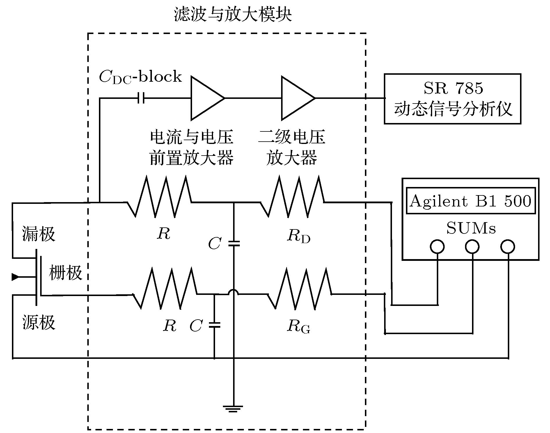
图 2 AlGaN/GaN HEMT器件的低频噪声测量系统[17]
Fig. 2. AlGaN/GaN HEMT devices’ low frequency noise measurement system.

图 3 零偏下AlGaN/GaN HEMT器件辐照前后输出特性曲线(a)与转移特性曲线(b)
Fig. 3. The output characteristic curve (a) and transfer characteristic curve (b) of the AlGaN/GaN HEMT device before and after irradiation under the zero-bias.
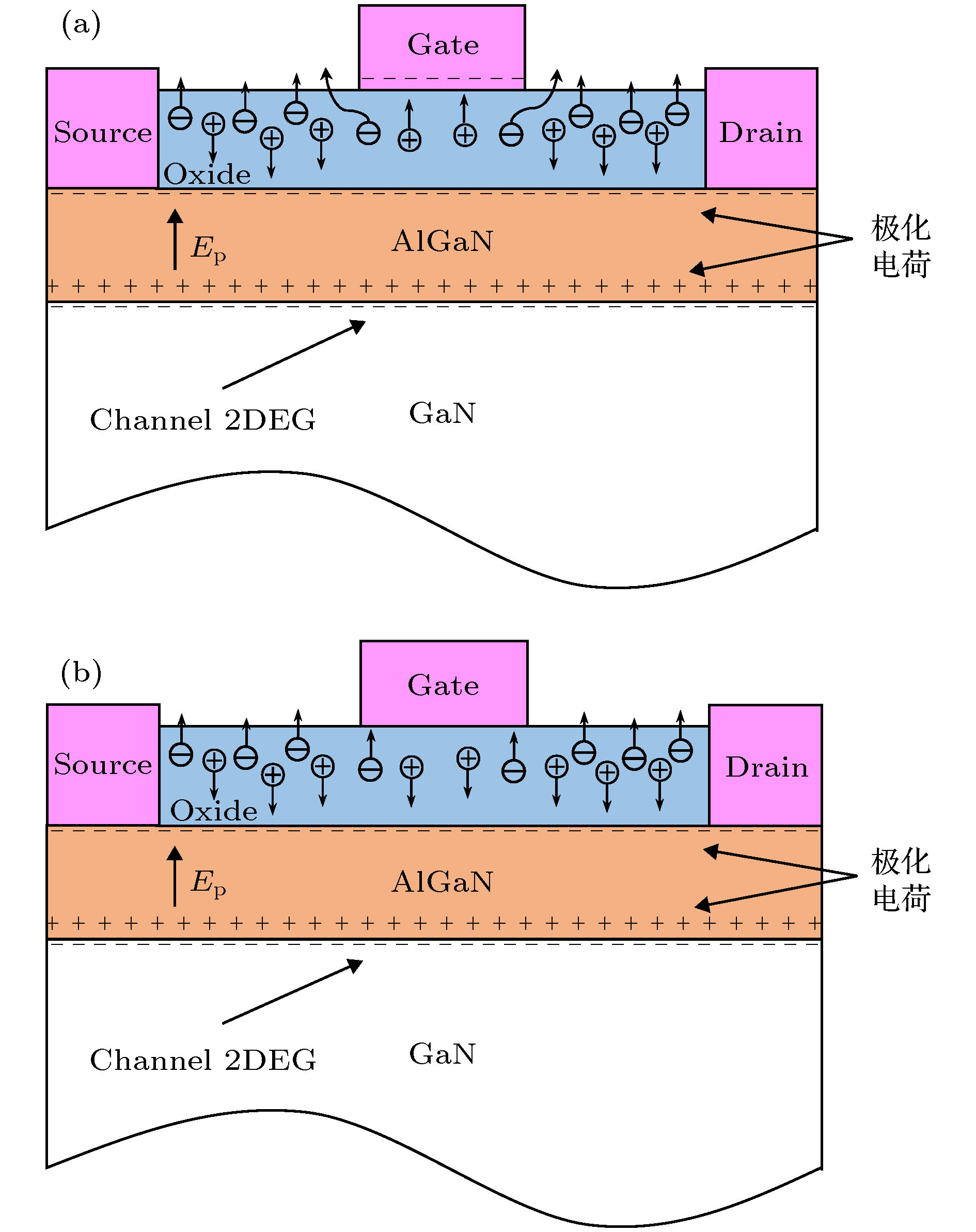
图 4 AlGaN/GaN HEMT器件辐照时的电荷分布图 (a)关态和半开态; (b)零偏
Fig. 4. Charge distribution patterns of AlGaN/GaN HEMT devices: (a) The off and semi-on states; (b) zero-bias.

图 5 AlGaN/GaN HEMT器件辐照前后沟道电流归一化噪声功率谱密度 (a)关态; (b)半开态; (c)零偏
Fig. 5. Normalized channel current noise power spectral density in the AlGaN/GaN HEMT devices before and after irradiation: (a) OFF state; (b) SEMI-ON state; (c) zero-bias.
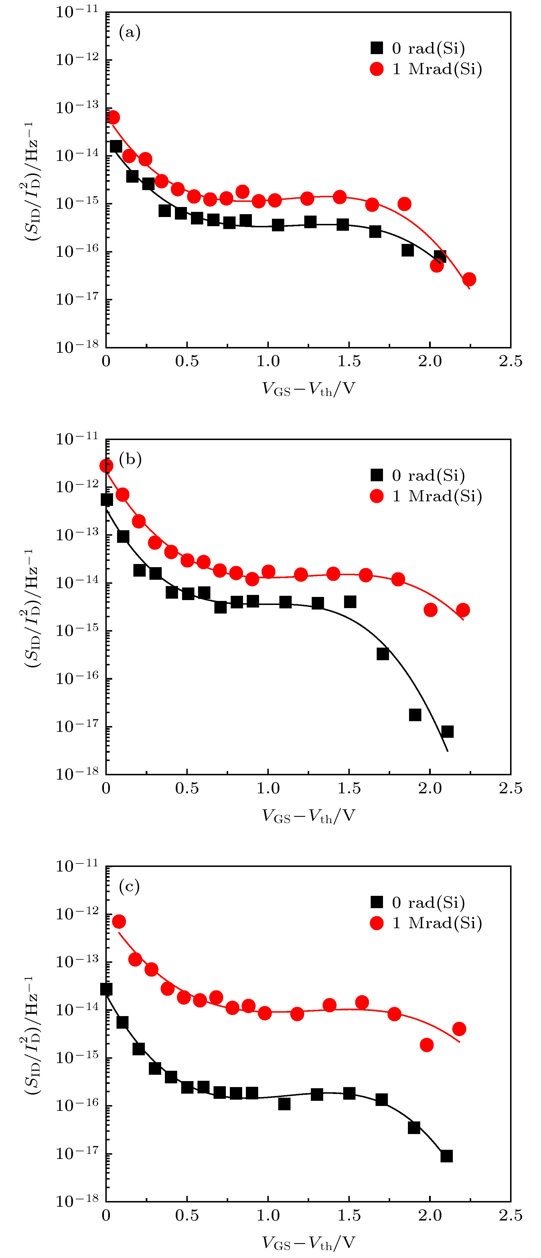
图 6 AlGaN/GaN HEMT器件辐照前后沟道电流归一化噪声功率谱密度随过驱动电压的变化(点: 测量值; 实线: 拟合值) (a)关态; (b)半开态; (c)零偏
Fig. 6. Normalized channel current noise power spectral density versus overdrive voltage in the AlGaN/GaN HEMT devices before and after irradiation: (a) OFF state; (b) SEMI-ON state; (c) zero-bias (dot: measured value; continuous line: fitted value).

图 7 AlGaN/GaN HEMT器件辐照前后沟道电流归一化噪声功率谱密度随沟道电流的变化(f = 25 Hz, 点: 测量值; 实线: 拟合值) (a)关态; (b); 半开态; (c)零偏
Fig. 7. Normalized channel current noise power spectral density versus channel current in the AlGaN/GaN HEMT devices before and after irradiation: (a) OFF state; (b) SEMI-ON state; (c) zero-bias (f = 25 Hz, dot: measured value; continuous line: fitted value).

图 8 AlGaN/GaN HEMT器件辐照前后势垒层内陷阱电荷密度的空间分布 (a)关态; (b)半开态; (c)零偏
Fig. 8. Extracted spatial distribution of trapped charges in the AlGaN/GaN HEMT devices’ barrier layer: (a) OFF state; (b) SEMI-ON state; (c) zero-bias.
表 1 AlGaN/GaN HEMT器件辐照实验偏置设置
Table 1. The biases set of AlGaN/GaN HEMT device irradiation experiment.
VGS/V VDS/V 关态(OFF) –3.0 0.5 半开态(SEMI-ON) –1.9 0.5 零偏(zero-bias) 0 0  下载: 导出CSV
表 2 不同偏置下AlGaN/GaN HEMT器件辐照前后饱和漏电流与最高跨导的变化
Table 2. Variation of saturation drain current and maximum transconductance before and after irradiation in AlGaN/GaNHEMT devices with different biases.
关态(OFF) 半开(SEMI-ON) 零偏(zero-bias) ΔIDSsat/% –26.00 –31.42 –36.28 Δgmmax/% –22.86 –34.58 –52.94
下载: 导出CSV
表 3 不同偏置下AlGaN/GaN HEMT器件辐照前后平带电压噪声功率谱密度(单位: V2·Hz–1)
Table 3. Flat-band voltage noise power spectral density in the AlGaN/GaN HEMT devices before and after irradiation under different biases (in V2·Hz–1).
关态
(OFF)半开态
(SEMI-ON)零偏
(zero-bias)0 rad(Si) 3.20 × 10⁻¹⁴ 2.65 × 10⁻¹⁴ 3.18 × 10⁻¹⁴ 1 Mrad(Si) 4.21 × 10⁻¹⁴ 3.85 × 10⁻¹⁴ 5.16 × 10⁻¹⁴
下载: 导出CSV
表 4 不同偏置下AlGaN/GaN HEMT器件辐照前后缺陷密度(单位: cm–3·eV–1)
Table 4. The defect density in the AlGaN/GaN HEMT devices before and after irradiation under different biases (in cm–3·eV–1).
关态
(OFF)半开态
(SEMI-ON)零偏
(zero-bias)0 rad(Si) 4.106 × 10¹⁷ 3.400 × 10¹⁷ 4.080 × 10¹⁷ 1 Mrad(Si) 5.402 × 10¹⁷ 4.940 × 10¹⁷ 6.621 × 10¹⁷ ΔNt/% 31.56 45.29 62.28
下载: 导出CSV
-
[1] 周幸叶, 吕元杰, 谭鑫, 王元刚, 宋旭波, 何泽召, 张志荣, 刘庆彬, 韩婷婷, 房玉龙, 冯志红 2018 物理学报 67 178501
Google Scholar
Zhou X Y, Lv Y J, Tan X, Wang Y G, Song X B, He Z Z, Zhang Z R, Liu Q B, Han T T, Fang Y L, Feng Z H 2018 Acta Phys. Sin. 67 178501
Google Scholar
[2] Vurgaftman I, Meyer J R, Ram-Mohan L R 2001 J. Appl. Phys. 89 5815
Google Scholar
[3] Meneghesso G, Verzellesi G, Rampazzo F, Zanon F, Tazzoli A, Meneghini M, Zanoni E 2008 IEEE Trans. Device Mater. Reliab. 8 332
Google Scholar
[4] Gong J M, Wang Q, Yan J D, Liu F Q, Feng C, Wang X L, Wang Z G 2016 Chin. Phys. Lett. 33 117303
Google Scholar
[5] Wu H, Duan B X, Yang L Y, Yang Y T 2019 Chin. Phys. B 28 027302
Google Scholar
[6] Zhang L, Lester L F, Baca A G, Shul R J, Chang P C, Willison C G, Mishra U K, Denbaars S P, Zolper J C 2000 IEEE Trans. Electron Devices 47 507
Google Scholar
[7] Jayarman R, Sodini C G 1989 IEEE Trans. Electron Devices 36 1773
Google Scholar
[8] Fleetwood D M, Shaneyfelt M R, Schwank J R 1994 Appl. Phys. Lett. 64 1965
Google Scholar
[9] 王凯, 刘远, 陈海波, 邓婉玲, 恩云飞, 张平 2015 物理学报 64 108501
Google Scholar
Wang K, Liu Y, Chen H B, Deng W L, En Y F, Zhang P 2015 Acta Phys. Sin. 64 108501
Google Scholar
[10] 刘远, 陈海波, 何玉娟, 王信, 岳龙, 恩云飞, 刘默寒 2015 物理学报 64 078501
Google Scholar
Liu Y, Chen H B, He Y J, Wang X, Yue L, En Y F, Liu M H 2015 Acta Phys. Sin. 64 078501
Google Scholar
[11] 孙鹏, 杜磊, 何亮, 陈文豪, 刘玉栋, 赵瑛 2012 物理学报 61 127808
Google Scholar
Sun P, Du L, He L, Chen W H, Liu Y D, Zhao Y 2012 Acta Phys. Sin. 61 127808
Google Scholar
[12] 刘远, 吴为敬, 李斌, 恩云飞, 王磊, 刘玉荣 2014 物理学报 63 098503
Google Scholar
Liu Y, Wu W J, Li B, En Y F, Wang L, Liu Y R 2014 Acta Phys. Sin. 63 098503
Google Scholar
[13] Fung T C, Baek G, Kanicki J 2010 J. Appl. Phys. 108 074518
Google Scholar
[14] Zheng X, Feng S W, Peng C, Lin G, Bai L, Li X, Yang Y, Pan S J, Hu Z X, Li X Y, Zhang Y M 2019 IEEE Trans. Electron Devices 66 3784
Google Scholar
[15] Smith M D, O’Mahony D, Vitobello F, Muschitiello M, Costantino A, Barnes A R, Parbrook P J 2016 Semicond. Sci. Technol. 31 025008
Google Scholar
[16] Bhuiyan M A, Zhou H, Chang S J, Lou X B, Gong X, Jiang R, Gong H Q, Zhang E X, Won C H, Lim J W, Lee J H, Gordon R G, Reed R A, Fleetwood D M, Ye P D, Ma T P 2017 IEEE Trans. Nucl. Sci. 65 46
Google Scholar
[17] Choi H S, Jeon S, Kim H, Shin J, Kim C, Chung U I 2011 IEEE Electron Device Lett. 32 1083
Google Scholar
[18] Rashmi A, Kranti S, Haldar, Gupta R S 2002 Solid State Electron. 46 621
Google Scholar
[19] 谷文萍, 张进城, 王冲, 冯倩, 马晓华, 郝跃 2009 物理学报 58 1161
Google Scholar
Gu W P, Zhang J C, Wang C, Feng Q, Ma X H, Hao Y 2009 Acta Phys. Sin. 58 1161
Google Scholar
[20] 吕玲 2013 博士学位论文 (西安: 西安电子科技大学)
Lü L 2013 Ph. D. Dissertation (Xi’an: Xidian University) (in Chinese)
[21] Hooge F N 1994 IEEE Trans. Electron Devices 41 1926
Google Scholar
[22] Simoen E, Mercha A, Claeys C, Lukyanchikova N 2007 Solid State Electron. 51 16
Google Scholar
[23] Jomaah J, Balestra 2004 IEE Proc. Circuits Devices Syst. 151 111
Google Scholar
[24] Liu Y, Wu W J, En Y F, Wang L, Lei Z F, Wang X H 2014 IEEE Electron Device Lett. 35 369
Google Scholar
[25] Ioannidis E G, Tsormpatzoglou A, Tassis D H, Dimitriadis C A, Templier F, Kamarinos G 2010 J. Appl. Phys. 108 106103
Google Scholar
[26] Ghibaudo G, Roux O, Nguyen-Duc C, Balestra F, Brini J 1991 Phys. Status Solidi A 124 571
Google Scholar
[27] Christensson S, Lundstrom I, Svensson C 1968 Solid State Electron. 11 797
Google Scholar
[28] Rahal M, Lee M, Burdett A P 2002 IEEE Trans. Electron Devices 49 319
Google Scholar

 下载:
下载:
计量
- 文章访问数: 15322
- PDF下载量: 250
- 被引次数: 0
