


-
雪崩光电二极管因其具有高的倍增被广泛应用于光通信、激光雷达等各种领域, 为了适应极微弱信号探测应用场合, 需要器件获得更高的增益值. 当前雪崩光电二极管一般采用单载流子倍增方式工作, 其倍增效果有限. 本文设计了一种电子和空穴同时参与倍增的InP/In0.53Ga0.47As/In0.52Al0.48As雪崩光电二极管结构, 其中吸收层采用In0.53Ga0.47As材料, 空穴倍增层采用InP材料, 电子倍增层采用In0.52Al0.48As材料, 两个倍增层分布在吸收层的上下两侧. 采用Silvaco TCAD软件对此结构以及传统单倍增层结构进行了模拟仿真, 对比单InP倍增层结构和单In0.52Al0.48As倍增层结构, 双倍增层结构在95%击穿电压下的增益值分别约为前两者的2.3倍和2倍左右, 由于两种载流子在两个倍增层同时参与了倍增, 所以器件具有更大的增益值, 且暗电流并没有增加, 有望提高系统探测的灵敏度.Avalanche photodiodes are widely used in various fields, such as optical communication and laser radar, because of their high multiplication. In order to adapt to very weak signal detection applications, devices are required to have higher gain values. The existing avalanche photodiodes generally use single carrier multiplication mode of operation, its multiplication effect is limited. In this paper is designed an InP/In0.53Ga0.47As/In0.52Al0.48As avalanche photodiode structure with electrons and holes jointly involved in multiplication. In this structure, In0.53Ga0.47As material is used for the absorption layer, InP material is used for the hole multiplication layer, In0.52Al0.48As is used for the electron multiplication layer, and the two multiplication layers are distributed on the upper side and lower side of the absorber layer. Under the reverse bias, the photogenerated electrons and the absorber-layer generated holes can enter into the respective multiplier layers in different directions and create the avalanche multiplication effect, so that the carriers are fully utilized. This structure and the conventional single multiplication layer structure are simulated by Silvaco TCAD software. Comparing the single InP multiplication layer structure with the single In0.52Al0.48As multiplication layer structure, the gain value of the double multiplication layer structure at 95% breakdown voltage is about 2.3 times and about 2 times of the former two, respectively, and the device has a larger gain value because both carriers are involved in multiplication in both multiplication layers at the same time. The structure has a dark current of 1.5 nA at 95% breakdown voltage, which does not increase in comparison with the single multiplication layer structure, owing to the effective control of the electric field inside the structure by multiple charge layers. Therefore, this structure is expected to improve the detection sensitivity of the system.
-
Keywords:
- avalanche photodiode /
- weak signal /
- dual carrier multiplication /
- gain
[1] Mccarthy A, Ren X, Della F A, Gemmell N R, Krichel N J, Scarcella C, Rugger A, Tosi A, Buller G S 2013 Opt. Express 21 22098
 Google Scholar
[2] Bertone N, Clark W 2007 Laser Focus World 43 69
[3] Mitra P, Beck J D, Skokan M R, Skokan M R, Robinson J E, Antoszewski J, Winchester K J, Keating A J, Nguyen T, Silva K, Musca C A, Dell J M, Faraone L 2006 SPIE Defense Commercial Sensing Orlando, United States, April 14–19, 2006 p70
[4] Tosi A, Calandri N, Sanzaro M, Acerbi F 2014 IEEE J. Sel. Top. Quant. 20 192
Google Scholar
[5] Jiang X, Itzler M, O’Donnell K, Entwistle M, Owens M, Slomkowski K, Rangwala S S 2014 IEEE J. Sel. Top. Quant. 21 5
Google Scholar
[6] Lee C, Johnson B, Molnar A C 2015 App. Phys. Lett. 106 231105
Google Scholar
[7] Nishida K, Taguchi K, Matsumoto Y 1979 App. Phys. Lett. 35 251
Google Scholar
[8] Li J, Dehzangi A, Brown G J, Razeghi M 2021 Sci. Rep. 11 7104
Google Scholar
[9] Tarof L E 1990 IEEE Photonic. Tech. L. 2 643
Google Scholar
[10] Campbell J C, Dentai A G, Holden W S, Kasper B L 1983 Electron. Lett. 19 818
Google Scholar
[11] Matsushima Y, Akiba S, Sakai K, Kushiro Y, Noda Y, Utaka K 1982 Electron. Lett. 22 945
Google Scholar
[12] Capasso F, Cho A Y, Foy P W 1984 Electron. Lett. 20 635
Google Scholar
[13] Forrest S R, Kim O K, Smith R G 1982 App. Phys. Lett. 41 95
Google Scholar
[14] Ma C, Deen M J, Tarof L E 1995 IEEE Trans. Electron Devices 42 2070
Google Scholar
[15] Emmons R B 1967 J. Appl. Phys. 38 3705
Google Scholar
[16] Mcintyre R J 1966 IEEE Trans. Electron Devices 13 164
Google Scholar
[17] 曾巧玉 2014 博士学位论文 (北京: 中国科学院大学)
Zeng Q Y 2014 Ph. D. Dissertation (Beijing: University of Chinese Academy of Sciences
[18] 吕粤希 2018 硕士学位论文 (北京: 中国科学院大学)
Lü Y X 2018 M. S. Thesis (Beijing: University of Chinese Academy of Sciences
[19] Cook L W, Bulman G E, Stillman G E 1982 App. Phys. Lett. 40 589
Google Scholar
[20] Goh Y L, Massey D, Marshall A R, Ng J S, Tan C H, Ng W K, Rees G J, Hopkinson M, David J P, Jones S 2007 IEEE Trans. Electron Devices 54 11
Google Scholar
[21] Capasso F, Mohammed K, Alavi K, Cho A Y, Foy P W 1984 App. Phys. Lett. 45 968
Google Scholar
[22] Melchior H, Hartman A R, Schinke D P, Seidel T E 1978 Bell Syst. Tech. J. 57 1791
Google Scholar
[23] Li X, Bamiedakis N, Wei J L, Penty R V, White I H 2014 Conference on Lasers and Electro-Optics (CLEO)—Laser Science to Photonic Applications San Jose, United States, June 8–13, 2014 p1
[24] Campbell J C 2004 IEEE J. Sel. Top. Quant. 10 777
Google Scholar
[25] Miller S L 1955 Phys. Rev. 99 1234
Google Scholar
[26] Ma C F, Deen M J, Tarof L E 1997 Adv. Imag. Elect. Phys. 99 65
Google Scholar
[27] Jones A H, March S D, Dadey A A, Muhowski A J, Bank S R, Campbell J C 2022 IEEE J. Quantum Electron. 58 1
Google Scholar
[28] Woodson M E, Ren M, Maddox S J, Chen Y, Bank S R, Campbell J C 2016 App. Phys. Lett. 108 081102
Google Scholar
[29] Huang J, Banerjee K, Ghosh S, Hayat M M 2013 IEEE Trans. Electron Devices 60 2296
Google Scholar
[30] Okuto Y, Crowell C R 1974 Phys. Rev. B 10 4284
Google Scholar
[31] 谢生, 张帆, 毛陆虹 2022 华中科技大学学报(自然科学版) 5 1
Google Scholar
Xie S, Zhang F, Mao L H 2022 J. Huazhong Univ. of Sci. & Tech. (Natural Science Edition) 5 1
Google Scholar
[32] Saleh M A, Hayat M M, Sotirelis P, Holmes A L, Campbell J C, Saleh B E, Teich M C 2001 IEEE Trans. Electron Devices 48 2722
Google Scholar
[33] 李慧梅 2016 硕士学位论文 (北京: 中国科学院大学)
Li H M 2016 M. S. Thesis (Beijing: University of Chinese Academy of Sciences
[34] Haško D, Kovác J, Uherek F, Škriniarová J, Jakabovic J, Peternai L 2006 Microelectron. J. 37 483
Google Scholar
-

图 1 双载流子倍增APD结构示意图
Fig. 1. Schematic diagram of double carrier multiplication APD structure.

图 4 结构Ⅰ在击穿电压下的电场分布
Fig. 4. Distribution of electric field at breakdown voltage for structure Ⅰ.

图 5 结构Ⅰ在击穿电压下的电离系数分布
Fig. 5. Distribution of ionization coefficient at breakdown voltage for structure Ⅰ.
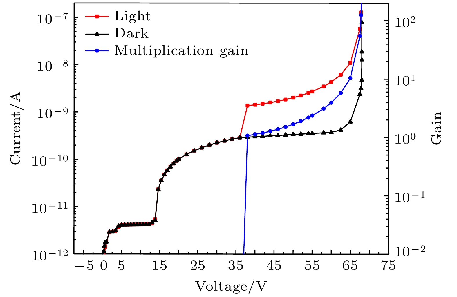
图 6 结构Ⅰ的I-V特性与增益曲线
Fig. 6. Currrent-voltage characteristics and gain of the structure Ⅰ.
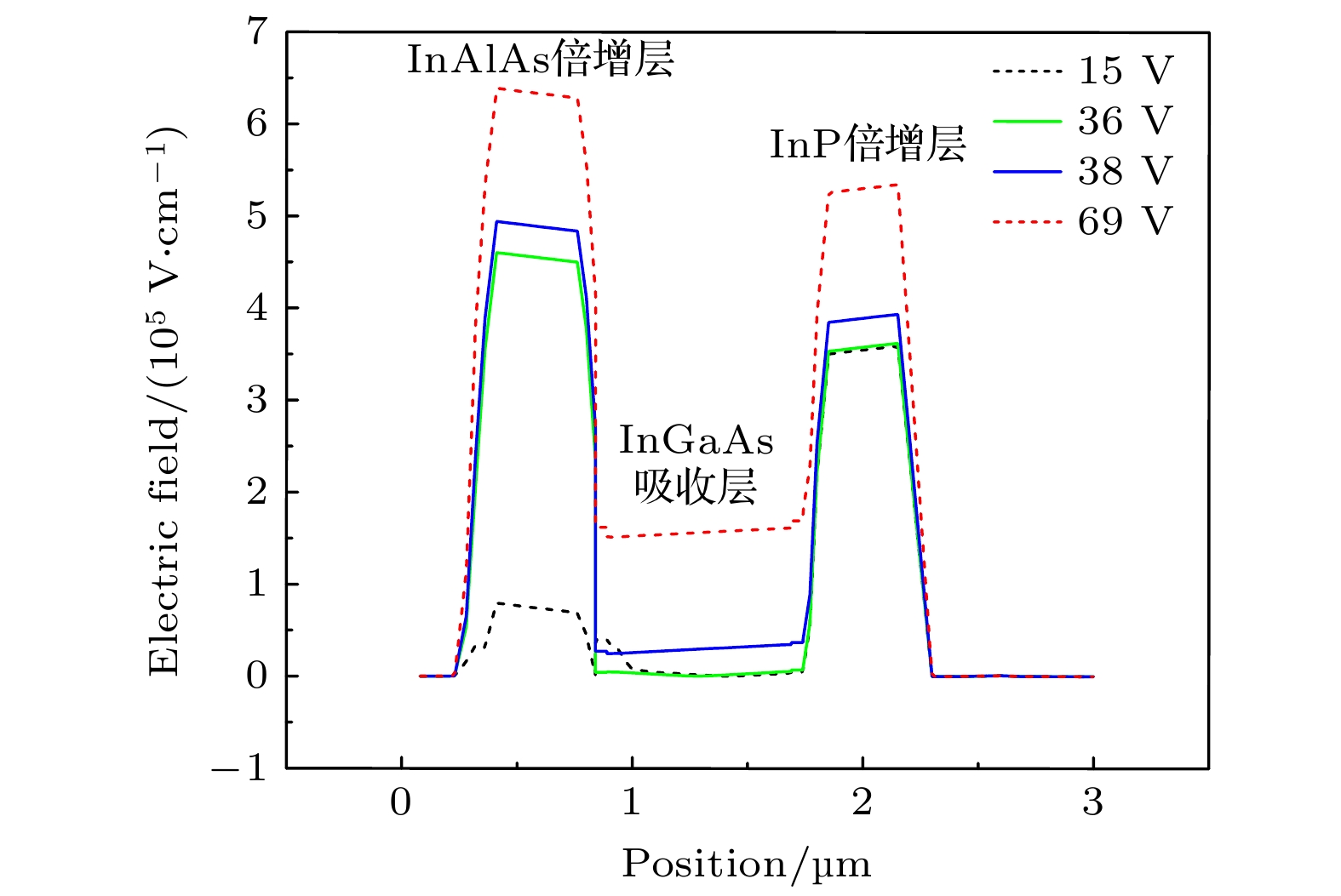
图 7 不同反向偏压下结构Ⅰ的电场分布
Fig. 7. Electric field distribution of structure Ⅰ under the different reverse bias voltage.

图 8 I-V特性与增益曲线 (a)结构Ⅱ; (b)结构Ⅲ
Fig. 8. Curve of I-V characteristics and gain: (a) Structure Ⅱ; (b) structure Ⅲ.
表 1 InAlAs和InP碰撞电离系数的仿真参数
Table 1. Simulation parameters for the ionization coefficients of InAlAs and InP.
材料 an/cm–1 ap/cm–1 bn/(V·cm–1) bp/(V·cm–1) InP 1.0×10⁷ 9.36×10⁷ 3.45×10⁶ 2.78×10⁶ InAlAs 6.2×10⁷ 1.00×10⁶ 4.00×10⁶ 4.00×10⁶  下载: 导出CSV
表 2 三种结构特性对比
Table 2. Comparison of the characteristics of three structures.
结构 击穿电压/V 暗电流/nA 增益 Ⅰ 69 1.5(@66 V) 35(@66 V) Ⅱ 44 2.0(@42 V) 15(@42 V) Ⅲ 45 1.5(@43 V) 18(@43 V)
下载: 导出CSV
-
[1] Mccarthy A, Ren X, Della F A, Gemmell N R, Krichel N J, Scarcella C, Rugger A, Tosi A, Buller G S 2013 Opt. Express 21 22098
Google Scholar
[2] Bertone N, Clark W 2007 Laser Focus World 43 69
[3] Mitra P, Beck J D, Skokan M R, Skokan M R, Robinson J E, Antoszewski J, Winchester K J, Keating A J, Nguyen T, Silva K, Musca C A, Dell J M, Faraone L 2006 SPIE Defense Commercial Sensing Orlando, United States, April 14–19, 2006 p70
[4] Tosi A, Calandri N, Sanzaro M, Acerbi F 2014 IEEE J. Sel. Top. Quant. 20 192
Google Scholar
[5] Jiang X, Itzler M, O’Donnell K, Entwistle M, Owens M, Slomkowski K, Rangwala S S 2014 IEEE J. Sel. Top. Quant. 21 5
Google Scholar
[6] Lee C, Johnson B, Molnar A C 2015 App. Phys. Lett. 106 231105
Google Scholar
[7] Nishida K, Taguchi K, Matsumoto Y 1979 App. Phys. Lett. 35 251
Google Scholar
[8] Li J, Dehzangi A, Brown G J, Razeghi M 2021 Sci. Rep. 11 7104
Google Scholar
[9] Tarof L E 1990 IEEE Photonic. Tech. L. 2 643
Google Scholar
[10] Campbell J C, Dentai A G, Holden W S, Kasper B L 1983 Electron. Lett. 19 818
Google Scholar
[11] Matsushima Y, Akiba S, Sakai K, Kushiro Y, Noda Y, Utaka K 1982 Electron. Lett. 22 945
Google Scholar
[12] Capasso F, Cho A Y, Foy P W 1984 Electron. Lett. 20 635
Google Scholar
[13] Forrest S R, Kim O K, Smith R G 1982 App. Phys. Lett. 41 95
Google Scholar
[14] Ma C, Deen M J, Tarof L E 1995 IEEE Trans. Electron Devices 42 2070
Google Scholar
[15] Emmons R B 1967 J. Appl. Phys. 38 3705
Google Scholar
[16] Mcintyre R J 1966 IEEE Trans. Electron Devices 13 164
Google Scholar
[17] 曾巧玉 2014 博士学位论文 (北京: 中国科学院大学)
Zeng Q Y 2014 Ph. D. Dissertation (Beijing: University of Chinese Academy of Sciences
[18] 吕粤希 2018 硕士学位论文 (北京: 中国科学院大学)
Lü Y X 2018 M. S. Thesis (Beijing: University of Chinese Academy of Sciences
[19] Cook L W, Bulman G E, Stillman G E 1982 App. Phys. Lett. 40 589
Google Scholar
[20] Goh Y L, Massey D, Marshall A R, Ng J S, Tan C H, Ng W K, Rees G J, Hopkinson M, David J P, Jones S 2007 IEEE Trans. Electron Devices 54 11
Google Scholar
[21] Capasso F, Mohammed K, Alavi K, Cho A Y, Foy P W 1984 App. Phys. Lett. 45 968
Google Scholar
[22] Melchior H, Hartman A R, Schinke D P, Seidel T E 1978 Bell Syst. Tech. J. 57 1791
Google Scholar
[23] Li X, Bamiedakis N, Wei J L, Penty R V, White I H 2014 Conference on Lasers and Electro-Optics (CLEO)—Laser Science to Photonic Applications San Jose, United States, June 8–13, 2014 p1
[24] Campbell J C 2004 IEEE J. Sel. Top. Quant. 10 777
Google Scholar
[25] Miller S L 1955 Phys. Rev. 99 1234
Google Scholar
[26] Ma C F, Deen M J, Tarof L E 1997 Adv. Imag. Elect. Phys. 99 65
Google Scholar
[27] Jones A H, March S D, Dadey A A, Muhowski A J, Bank S R, Campbell J C 2022 IEEE J. Quantum Electron. 58 1
Google Scholar
[28] Woodson M E, Ren M, Maddox S J, Chen Y, Bank S R, Campbell J C 2016 App. Phys. Lett. 108 081102
Google Scholar
[29] Huang J, Banerjee K, Ghosh S, Hayat M M 2013 IEEE Trans. Electron Devices 60 2296
Google Scholar
[30] Okuto Y, Crowell C R 1974 Phys. Rev. B 10 4284
Google Scholar
[31] 谢生, 张帆, 毛陆虹 2022 华中科技大学学报(自然科学版) 5 1
Google Scholar
Xie S, Zhang F, Mao L H 2022 J. Huazhong Univ. of Sci. & Tech. (Natural Science Edition) 5 1
Google Scholar
[32] Saleh M A, Hayat M M, Sotirelis P, Holmes A L, Campbell J C, Saleh B E, Teich M C 2001 IEEE Trans. Electron Devices 48 2722
Google Scholar
[33] 李慧梅 2016 硕士学位论文 (北京: 中国科学院大学)
Li H M 2016 M. S. Thesis (Beijing: University of Chinese Academy of Sciences
[34] Haško D, Kovác J, Uherek F, Škriniarová J, Jakabovic J, Peternai L 2006 Microelectron. J. 37 483
Google Scholar

 下载:
下载:


计量
- 文章访问数: 1332
- PDF下载量: 48
- 被引次数: 0
