


-
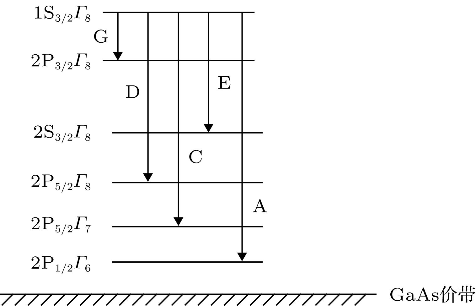
通过远红外吸收谱、光致发光光谱和拉曼散射光谱, 对均匀掺杂在GaAs材料中Be受主能级之间的跃迁进行了研究. 实验中使用的GaAs:Be样品是通过分子束外延设备, 生长在半绝缘(100) GaAs衬底之上的外延单层. 在4.2 K温度下, 对样品分别进行了远红外吸收光谱、光致发光光谱、Raman光谱的实验测量. 在远红外吸收光谱中, 清楚地观察到了从Be受主1S3/2Γ8基态到它的三个激发态2P3/2Γ8, 2P5/2Γ8和2P5/2Γ7之间的奇宇称跃迁吸收峰. 跃迁能量与先前文献中报道的符合得很好. 从光致发光光谱中, 观察到了Be受主从1S3/2Γ8基态到2S3/2Γ8激发态的两空穴跃迁的发光峰, 从而间接地找到了两能级之间的跃迁能量. 在Raman光谱中, 清楚地分辨出来了Be受主从1S3/2Γ8基态到2S3/2Γ8激发态偶宇称跃迁的拉曼散射峰, 直接得到了两能级间的跃迁能量. 对比发现, 分别直接和间接得到的1S3/2Γ8基态到2S3/2Γ8激发态跃迁能量结果是一致的.The doping is one of important means in the semiconductor manufacturing techniques, by which the optical and electric properties of semiconductor materials can be significantly improved. The doping level and energy level structure of dopants have a great influence on the operating performances of micro-electronic devices. Beryllium is one of acceptors, which is frequently used to be doped in GaAs bulk, because it is very stable with respect to diffusion at higher temperatures. Therefore, it is significant for the application to optoelectronic devices that the energy-state structure of Be acceptors in GaAs bulk can be investigated in detail. The sample GaAs:Be used in experiment is a 5-μm-thick epitaxial single layer doped uniformly by Be acceptors with a doping level of 2 × 1016 cm–3, and grown by molecular beam epitaxy on 450-μm-thick semi-insulating (100) GaAs substrates in a VG V80 H reactor equipped with all solid sources. The transitions between the energy states of Be acceptors are studied experimentally by different spectroscopy techniques. The far-infrared absorption experiments are performed by using a Fourier-transform spectrometer equipped with a tungsten light source and a multilayer wide band beam splitter. Prior to the absorption spectrum measurement, the sample is thinned, polished and wedged to approximately a 5° angle to suppress optical interference between the front and back faces. Then, the sample is placed into the cryostat with liquid helium (4.2 K). The photoluminescence and Raman spectra are also measured at 4.2 K by a Renishaw Raman imaging microscope. The optical excitation to the sample is provided by an argon-ion laser with a wavelength of 514.5 nm, and the excited power is typically 5 mW. The odd-parity transitions from the Be acceptor ground state 1S3/2Γ8 to three excited states, i.e. 2P3/2Γ8, 2P5/2Γ8 and 2P5/2Γ7 are clearly observed in the far-infrared absorption spectra, then the respective transition energy values are obtained, which are in excellent agreement with the experimental results reported previously. In the photoluminescence spectrum, the emission peak labelled two holetransition, originating from the two-hole transition of recombination of the neutral-accptor bound excitons, is seen obviously, thus the energy of the even-parity transition between 1S3/2Γ8 and 2S3/2Γ8 states is found indirectly. Furthermore, in the Raman spectrum measured, the transition peak between 1S3/2Γ8 and 2S3/2Γ8 states is well resolved, and the transition energy between them is gained directly. By comparison, the transition energy values gained directly and indirectly are found to be consistent with each other.
-
Keywords:
- far-infrared absorption spectrum /
- Raman spectrum /
- photoluminescence spectrum /
- energy state structure of Be acceptor
[1] Park J, Barnes P A, Lovejoy M L 1995 Appl. Phys. Lett. 67 968
 Google Scholar
[2] Jiang D S, Makita Y, Ploog K, Queisser H J 1982 J. Appl. Phys. 53 999
Google Scholar
[3] Arab S, Yao M, Zhou C, Dapkus P D, Cronin S B 2016 Appl. Phys. Lett. 108 182106
Google Scholar
[4] Hu J, Zhang H, Sun Y, Misochko O V, Nakamura K G 2018 Phys. Rev. B 97 165307
Google Scholar
[5] Belykh V V, Kavokin K V, Yakovlev D R, Bayer M 2017 Phys. Rev. B 96 241201
Google Scholar
[6] Donnelly J P, Leonberger F J, Bozler C O 1976 Appl. Phys. Lett. 28 706
Google Scholar
[7] Waldrop J R 1988 Appl. Phys. Lett. 53 1518
Google Scholar
[8] Beyzavi K, Lee K, Kim D M, Nathan M I, Wrenner K, Wright S L 1991 Appl. Phys. Lett. 58 1268
Google Scholar
[9] Wagner J, Seelewind H, Koidl P 1986 Appl. Phys. Lett. 49 1080
Google Scholar
[10] Atzmuller R, Dahl M, Kraus J, Schaack G, Schubert J 1991 J. Phys. Condens. Matter 3 6775
Google Scholar
[11] Sze S M 1981 Physics of Semiconductor Devices (New York: John Wiley & Sons Ltd.) p20
[12] Reeder A A, McCombe B D, Chambers F A, Devane G P 1988 Phys. Rev. B 38 4318
Google Scholar
[13] Reeder A A, McCombe B D, Chambers F A, Devane G P 1988 Superlatt. Microstruct. 4 381
Google Scholar
[14] Reeder A A, Mercy J M, McCombe B D 1988 IEEE J. Quantum Electron. 24 1690
Google Scholar
[15] Lewis R A, Cheng T S, Henini M, Chamberlain J M 1996 Phys. Rev. B 53 12829
Google Scholar
[16] Wan K, Bray R M 1985 Phys. Rev. B 32 5265
Google Scholar
[17] Gammon D, Merlin R, Masselink W T, Morkoc H 1986 Phys. Rev. B 33 2919
Google Scholar
[18] Lipari N O, Balderschi A 1978 Solid State Commun. 25 665
Google Scholar
[19] Balderschi A, Lipari N O 1976 Journal of Luminescence 12−13 489
[20] Fiorentini V, Balderschi A 1989 Solid State Commun. 69 953
Google Scholar
[21] Fisher P, Fan H Y 1959 Phys. Rev. Lett. 2 456
Google Scholar
[22] Kirkman R F, Stradling R A, Lin-Chung P J 1978 J. Phys. C 11 419
Google Scholar
[23] Luttinger J M 1956 Phys. Rev. 102 1030
Google Scholar
[24] Balderschi A, Lipari N O 1973 Phys. Rev. B 8 2697
Google Scholar
[25] Balderschi A, Lipari N O 1974 Phys. Rev. B 9 1525
Google Scholar
[26] Labrie D, Booth I J, Thewalt M L W, Clayman B P 1986 Appl. Opt. 25 171
Google Scholar
[27] Koteles E S, Datars W R 1976 Can. J. Phys. 54 1676
Google Scholar
[28] Shen X C 2002 Spectrum and Optical Property of Semiconductor (Beijing: Scientific Press) p553 (in Chinese) [沈学础 2002 半导体光谱和光学性质 (北京: 科学出版社) 第553页]
[29] Contour J P, Neu G, Leroux M, Chaix C, Levesque B, Etienne P 1983 J. Vac. Sci. Technol. B 1 811
[30] Bhattacharya P K, BOhlmann H J, Iegems M 1982 J. Appl. Phys. 53 6391
Google Scholar
[31] Wan K, Young J F, Devine R L S, Moore W T, Thorpe S, Miner C J, Mandeville P 1988 J. Appl. Phys. 63 5598
Google Scholar
[32] Olego D, Cardona M 1981 Phys. Rev. B 24 7217
Google Scholar
-
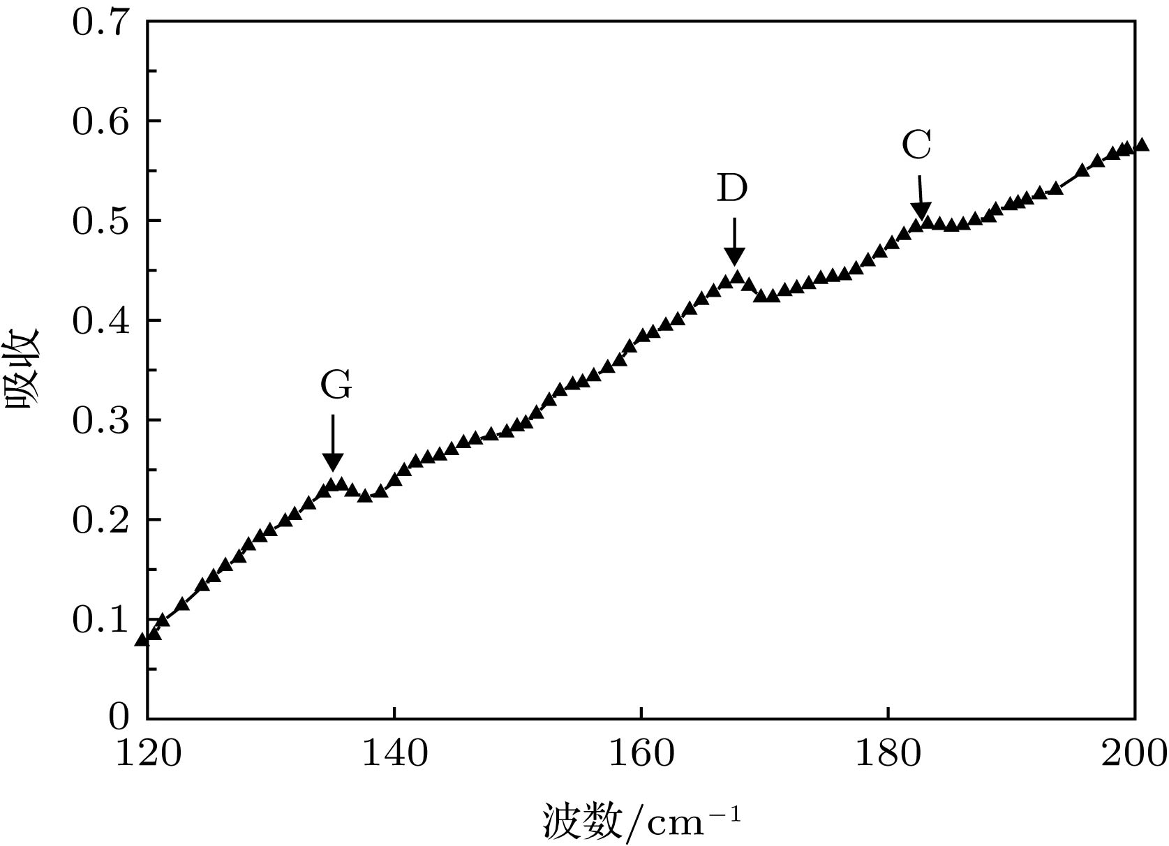
图 2 在4.2 K温度下, GaAs:Be样品的远红外吸收谱
Fig. 2. Far-infrared absorption spectrum for the sample GaAs:Be at 4.2 K.
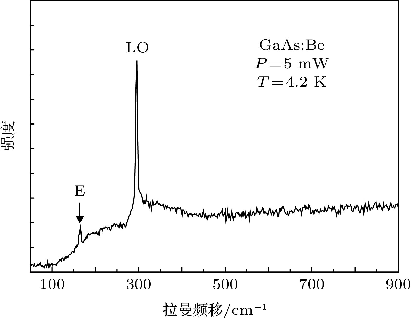
图 4 在4.2 K温度下, GaAs:Be样品的Raman光谱
Fig. 4. Raman spectrum of the sample GaAs:Be at 4.2 K.
-
[1] Park J, Barnes P A, Lovejoy M L 1995 Appl. Phys. Lett. 67 968
Google Scholar
[2] Jiang D S, Makita Y, Ploog K, Queisser H J 1982 J. Appl. Phys. 53 999
Google Scholar
[3] Arab S, Yao M, Zhou C, Dapkus P D, Cronin S B 2016 Appl. Phys. Lett. 108 182106
Google Scholar
[4] Hu J, Zhang H, Sun Y, Misochko O V, Nakamura K G 2018 Phys. Rev. B 97 165307
Google Scholar
[5] Belykh V V, Kavokin K V, Yakovlev D R, Bayer M 2017 Phys. Rev. B 96 241201
Google Scholar
[6] Donnelly J P, Leonberger F J, Bozler C O 1976 Appl. Phys. Lett. 28 706
Google Scholar
[7] Waldrop J R 1988 Appl. Phys. Lett. 53 1518
Google Scholar
[8] Beyzavi K, Lee K, Kim D M, Nathan M I, Wrenner K, Wright S L 1991 Appl. Phys. Lett. 58 1268
Google Scholar
[9] Wagner J, Seelewind H, Koidl P 1986 Appl. Phys. Lett. 49 1080
Google Scholar
[10] Atzmuller R, Dahl M, Kraus J, Schaack G, Schubert J 1991 J. Phys. Condens. Matter 3 6775
Google Scholar
[11] Sze S M 1981 Physics of Semiconductor Devices (New York: John Wiley & Sons Ltd.) p20
[12] Reeder A A, McCombe B D, Chambers F A, Devane G P 1988 Phys. Rev. B 38 4318
Google Scholar
[13] Reeder A A, McCombe B D, Chambers F A, Devane G P 1988 Superlatt. Microstruct. 4 381
Google Scholar
[14] Reeder A A, Mercy J M, McCombe B D 1988 IEEE J. Quantum Electron. 24 1690
Google Scholar
[15] Lewis R A, Cheng T S, Henini M, Chamberlain J M 1996 Phys. Rev. B 53 12829
Google Scholar
[16] Wan K, Bray R M 1985 Phys. Rev. B 32 5265
Google Scholar
[17] Gammon D, Merlin R, Masselink W T, Morkoc H 1986 Phys. Rev. B 33 2919
Google Scholar
[18] Lipari N O, Balderschi A 1978 Solid State Commun. 25 665
Google Scholar
[19] Balderschi A, Lipari N O 1976 Journal of Luminescence 12−13 489
[20] Fiorentini V, Balderschi A 1989 Solid State Commun. 69 953
Google Scholar
[21] Fisher P, Fan H Y 1959 Phys. Rev. Lett. 2 456
Google Scholar
[22] Kirkman R F, Stradling R A, Lin-Chung P J 1978 J. Phys. C 11 419
Google Scholar
[23] Luttinger J M 1956 Phys. Rev. 102 1030
Google Scholar
[24] Balderschi A, Lipari N O 1973 Phys. Rev. B 8 2697
Google Scholar
[25] Balderschi A, Lipari N O 1974 Phys. Rev. B 9 1525
Google Scholar
[26] Labrie D, Booth I J, Thewalt M L W, Clayman B P 1986 Appl. Opt. 25 171
Google Scholar
[27] Koteles E S, Datars W R 1976 Can. J. Phys. 54 1676
Google Scholar
[28] Shen X C 2002 Spectrum and Optical Property of Semiconductor (Beijing: Scientific Press) p553 (in Chinese) [沈学础 2002 半导体光谱和光学性质 (北京: 科学出版社) 第553页]
[29] Contour J P, Neu G, Leroux M, Chaix C, Levesque B, Etienne P 1983 J. Vac. Sci. Technol. B 1 811
[30] Bhattacharya P K, BOhlmann H J, Iegems M 1982 J. Appl. Phys. 53 6391
Google Scholar
[31] Wan K, Young J F, Devine R L S, Moore W T, Thorpe S, Miner C J, Mandeville P 1988 J. Appl. Phys. 63 5598
Google Scholar
[32] Olego D, Cardona M 1981 Phys. Rev. B 24 7217
Google Scholar

 下载:
下载:

计量
- 文章访问数: 10538
- PDF下载量: 59
- 被引次数: 0
