-
磁电阻作为表征自旋阀结构最具代表性的特征之一, 是研究多层膜层间耦合作用的重要研究手段. 稀土/磁性过渡金属通过耦合和界面效应诱导室温下稀土具有磁性, 插入中间非磁金属层通过调控层间耦合作用实现自旋阀结构将有利于拓展稀土在自旋电子学领域的应用. 通过分析具有不同Cr层厚度(tCr)的Gd (4 nm)/Cr(tCr)/FeCo (5 nm)三层膜室温下面内磁电阻效应, 本文研究了薄膜的层间耦合和界面效应. 研究发现, 相对于FeCo薄膜, Gd/FeCo薄膜表现出更为明显的各向异性磁电阻. Cr的插入使得电流垂直于磁场时的磁电阻在低场峰值位置处出现一极小值, 且这个极小值随着tCr的增加变得更加明显. 当tCr = 3 nm时, 几乎完全表现为负自旋阀磁电阻效应. FeCo层与Cr/Gd形成的不同的自旋散射不对称是产生这一负自旋阀磁电阻效应的主要原因. 电流平行于磁场时磁电阻峰值随tCr的振荡和低温下的磁滞回线证实了低温和室温下层间耦合的存在.As one of the most representative features characterizing the spin valve structure, magnetoresistance is an important method to study the interlayer coupling in multilayers. Considering the induced magnetism of rare earth at room temperature due to the coupling and magnetic proximity effect in the structure of rare earth/magnetic transition metal, an intermediate nonmagnetic metal can be inserted to form the spin valve structure to regulate the interlayer coupling, which expands the scope of applications of rare earth in spintronics. In this work, the interlayer exchange coupling and interfacial effects of Gd (4 nm)/Cr (tCr)/FeCo (5 nm) trilayers with different Cr layer thickness (tCr) are studied by means of in plane magnetoresistance. Compared with FeCo film, Gd/FeCo film obtains more obvious anisotropic magnetoresistance. While the magnetoresistance value obtained for the configuration of I⊥H shows a minimum value at the peak due to the insertion of Cr layer, and this minimum value becomes more pronounced with the increase of tCr. When tCr = 3 nm, the negative spin valve effect almost totally overcomes the anisotropic-magnetoresistance effect. Different spin asymmetries of scattering that are formed in FeCo layer and Cr/Gd layers are mainly responsible for creating the negative spin valve magnetoresistance, in which the resistance becomes smaller near the coercive, while the resistance becomes larger at high field parallel to magnetic moment. The oscillation of magnetoresistance with tCr at I // H and the hysteresis loops at 5 K further confirm the existence of interlayer coupling both at room temperature and 5 K.
-
Keywords:
- FeCo film /
- magnetoresistance /
- interlayer coupling /
- rare earth
[1] Lee J C T, Chess J J, Montoya S A, Shi X, Tamura N, Mishra S K, Fischer P, McMorran B J, Sinha S K, Fullerton E E, Kevan S D, Roy S 2016 Appl. Phys. Lett. 109 022402
 Google Scholar
[2] Talapatra A, Chelvane J A, Satpati B, Kumar S, Mohanty J 2019 J. Alloy. Compd. 774 1059
 Google Scholar
[3] Bhatt R C, Liao C M, Ye L X, Hai N T, Wu J C, Wu T H 2021 J. Magn. Magn. Mater. 526 167734
 Google Scholar
[4] Inyang O, Rafiq A, Swindells C, Ali S, Atkinson D 2020 Sci. Rep. 10 9767
 Google Scholar
[5] Kirk E, Bull C, Finizio S, et al. 2020 Phys. Rev. Mater. 4 074403
 Google Scholar
[6] Huang M, Qiu Z, Wang F, Luo H, Zhang J 2022 J. Alloy. Compd. 901 163619
 Google Scholar
[7] Ming X, Han X, Yang M, Yan G 2022 J. Magn. Magn. Mater. 550 169064
 Google Scholar
[8] Jin H M 1983 J. Magn. Magn. Mater. 35 283
 Google Scholar
[9] Elhamali S M, Ibrahim N B, Radiman S 2018 Mater. Chem. Phys. 208 1
 Google Scholar
[10] Talapatra, Chelvane J A, Mohanty J 2021 J. Alloy. Compd. 861 157953
 Google Scholar
[11] Wang K, Tang Y, Zhang K, Wang Y, Liu J 2021 Mater. Sci. Eng. B-Adv. 263 114848
 Google Scholar
[12] Basumatary H, Chelvane J A, Rao D V S, Talapatra A, Mohanty J, Kumar D, Singh V, Kamat S V, Ranjan R 2021 J. Alloy. Compd. 869 159571
 Google Scholar
[13] Bhatt R C, Ye L X, Hai N T, Wu J C, Wu T H 2021 J. Magn. Magn. Mater. 537 168196
 Google Scholar
[14] Stanciu A E, Schinteie G, Kuncser A, Iacob N, Trupina L, Ionita I, Crisan O, Kuncser V 2020 J. Magn. Magn. Mater. 498 166173
 Google Scholar
[15] Morishita T, Togami Y, Tsushima K 1986 J. Magn. Magn. Mater. 54–57 789
 Google Scholar
[16] Frąckowiak Ł, Stobiecki F, Urbaniak M, Matczak M, Chaves-O`Flynn G D, Bilski M, Glenz A, Kuświk P 2022 J. Magn. Magn. Mater. 544 168682
 Google Scholar
[17] Wang J, Li C, Wang Y, Tang R, Chai G, Jiang C 2021 Appl. Surf. Sci. 567 150527
 Google Scholar
[18] Rebei A, Hohlfeld J 2006 Phys. Rev. Lett. 97 117601
 Google Scholar
[19] 高瑞鑫, 徐振, 陈达鑫, 徐初东, 陈志峰, 刘晓东, 周仕明, 赖天树 2009 物理学报 58 580
 Google Scholar
Gao R X, Xu Z, Chen D X, Xu C D, Chen Z F, Liu X D, Zhou S M, Lai T S 2009 Acta Phys. Sin. 58 580
 Google Scholar
[20] Sun L, Yue J J, Jiang S, Xu Y J, Li Q N, Chen Q, Zhou X C, Huang Z C, Yao Z Y, Zhai Y, Zhai H R 2017 J. Alloy. Compd. 695 1324
 Google Scholar
[21] Guo H S, Li L Z, Wu X H, Zhong Z C, Tao Z X, Wang F H, Wang T 2021 J. Magn. Magn. Mater. 538 168249
 Google Scholar
[22] Ceballos A, Pattabi A, El-Ghazaly A, Ruta S, Simon C P, Evans R F L, Ostler T, Chantrell R W, Kennedy E, Scott M, Bokor J, Hellman F 2021 Phys. Rev. B 103 024438
 Google Scholar
[23] 侯育花, 黄有林, 刘仲武, 曾德长 2015 物理学报 64 037501
 Google Scholar
Hou Y H, Huang Y L, Liu Z W, Zeng D C 2015 Acta Phys. Sin. 64 037501
 Google Scholar
[24] Hao A, Ismail M, He S, Qin N, Chen R, Rana A M, Bao D 2018 Mater. Sci. Eng. B-Adv. 229 86
 Google Scholar
[25] Chakrabarty S, Sinha A, Dutta A, Pal M 2018 J. Magn. Magn. Mater. 468 215
 Google Scholar
[26] Bulai G, Trandafir V, Irimiciuc S A, Ursu L, Focsa C, Gurlui S 2019 Ceram. Int. 45 20165
 Google Scholar
[27] Bohr C, Yu P, Scigaj M, Hegemann C, Fischer T, Coll M, Mathur S 2020 Thin Solid Films 698 137848
 Google Scholar
[28] Sharma S, Verma M K, Sharma N D, Choudhary N, Singh S, Singh D 2021 Ceram. Int. 47 17510
 Google Scholar
[29] Li N, Tang J, Su L, Ke Y J, Zhang W, Xie Z K, Sun R, Zhang X Q, He W, Cheng Z H 2021 Chin. Phys. B 30 117502
 Google Scholar
[30] Shan Z S, Sellmyer D J 1990 Phys. Rev. B 42 10433
 Google Scholar
[31] Kim W S, Andrä W, Kleemann W 1998 Phys. Rev. B 58 6346
 Google Scholar
[32] Schmidt T, Hoffmann H 2002 J. Magn. Magn. Mater. 248 181
 Google Scholar
[33] Drovosekov A B, Savitsky A O, Kholin D I, Kreines N M, Proglyado V V, Makarova M V, Kravtsov E A, Ustinov V V 2019 J. Magn. Magn. Mater. 475 668
 Google Scholar
[34] Xiang O, Xiong C, Wang Z, Zhang Y, Xu Y, Yi L, Piao H G, Pan L 2020 J. Magn. Magn. Mater. 516 167334
 Google Scholar
[35] Basha M A, Prajapat C L, Bhatt H, Kumar Y, Gupta M, Kinane C J, Cooper J F K, Langridge S, Basu S, Singh S 2020 J. Magn. Magn. Mater. 516 167331
 Google Scholar
[36] Mattson J E, Sowers C H, Berger A, Bader S D 1992 Phys Rev Lett. 68 3252
 Google Scholar
[37] Bellouard C, George B, Marchal G, Maloufi N, Eugène J 1997 J. Magn. Magn. Mater. 165 312
 Google Scholar
[38] Sun L, Li X Y, Zhao X C, Ban D M, Li G J, Yao Z H, Zhao Z B, Zhai Y, Cui X Y 2021 J Mater Sci: Mater Electron 32 28245
 Google Scholar
[39] George J M, Pereira L G, Barthélémy A, Petroff F, Steren L, Duvail J L, Fert A, Loloee R, Holody P, Schroeder P A 1994 Phys. Rev. Lett. 72 408
 Google Scholar
[40] Renard J P, Bruno P, Mégy R, Bartenlian B, Beauvillain P, Chappert C, Dupas C, Kolb E, Mulloy M, Veillet P, Vélu E 1995 Phys. Rev. B 51 12821
 Google Scholar
[41] Sanyal B, Antoniak C, Burkert T, Krumme B, Warland A, Stromberg F, Praetorius C, Fauth K, Wende H, Eriksson O 2010 Phys. Rev. Lett. 104 156402
 Google Scholar
[42] Scheunert G, Hendren W R, Ward C, Bowman R M 2012 App. Phys. Lett. 101 142407
 Google Scholar
[43] Liu Y F, Cai J W, Sun L 2010 Appl. Phys. Lett. 96 092509
 Google Scholar
[44] Jiao Z, Chen H, Jiang W, Wang J, Zhou Y, Yu S, Hou Y, Ye Q 2015 Mater. Lett. 158 241
 Google Scholar
[45] Zhao W, Liu C, Huang W, Hou C, Chen Z, Luo Z, Yin Y, Li X 2019 Mater. Lett. 240 124
 Google Scholar
[46] Peng C, Chen D, Dai D 1993 Solid State Commun. 87 161
 Google Scholar
[47] Parkin S S P, More N, Roche K P 1990 Phys, Rev. Lett. 64 2304
 Google Scholar
[48] Parkin S S P, Bhadra R, Roche K P 1991 Phys. Rev. Lett. 66 2152
 Google Scholar
-
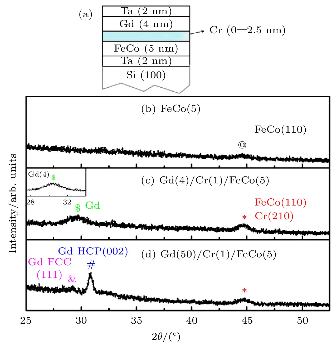
图 1 (a) Si(100)衬底上生长的Gd/Cr/FeCo结构示意图, 2 nm Ta作为保护层和缓冲层; (b)—(d) FeCo (5 nm)薄膜和不同厚度Gd层的Gd/Cr (1 nm)/FeCo (5 nm) 薄膜的 XRD图谱 (图1(c)插图是Ta (2 nm)/Gd (4 nm)/Ta (2 nm) 薄膜的Gd衍射峰)
Fig. 1. (a) Schematic diagram of the film structure for Gd/Cr/FeCo on Si(100) with Ta (2 nm) as the capping layer and buffering layer; (b)–(d) XRD patterns for the FeCo (5 nm) and Gd/Cr (1 nm)/FeCo (5 nm) films with different thickness of Gd layer. (The inset of Fig. 1(c) shows the diffraction peak of Gd for Ta (2 nm)/Gd (4 nm)/Ta (2 nm) film).
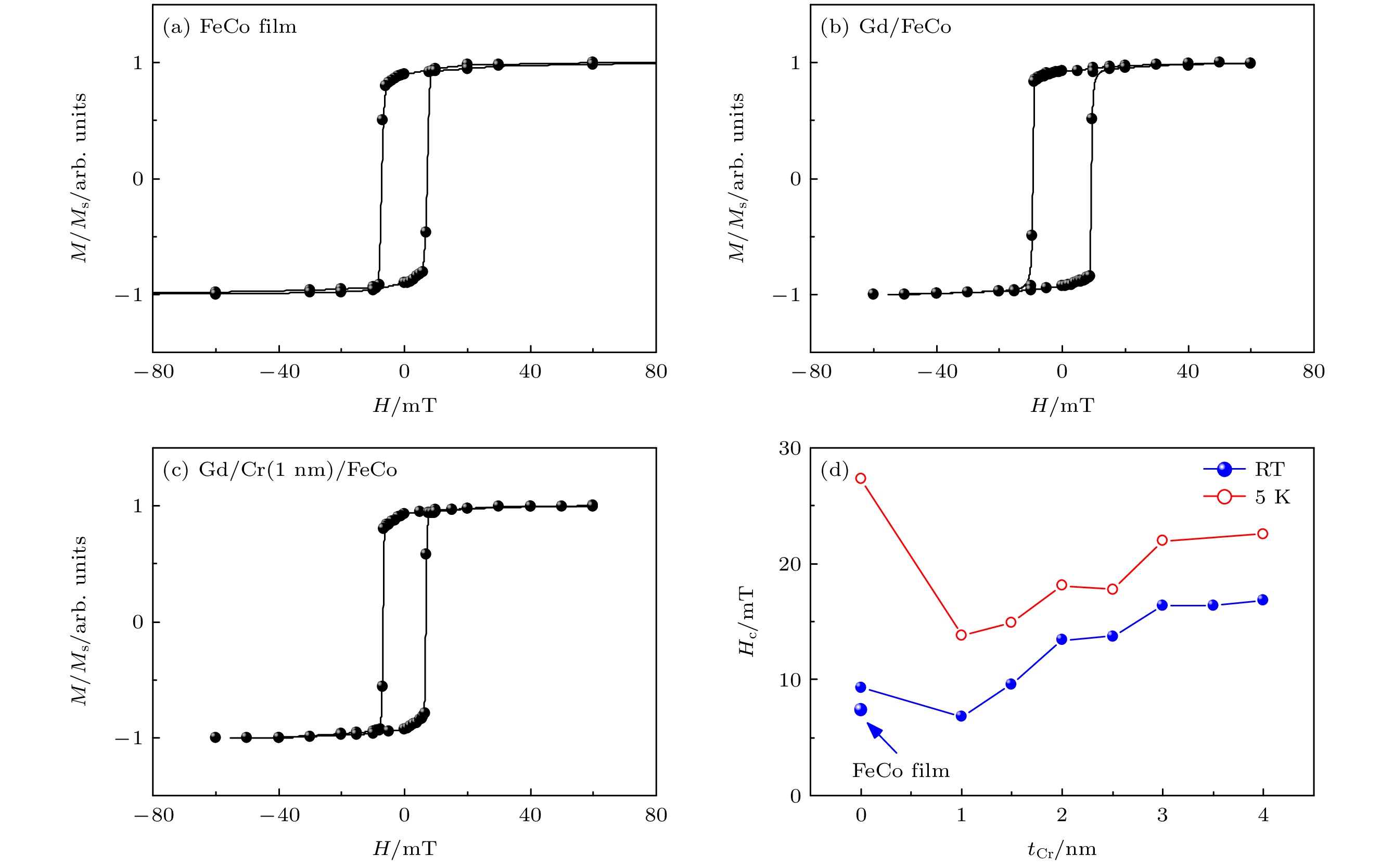
图 2 (a)—(c) 具有代表性的薄膜在室温下的面内磁滞回线; (d) 室温和 5 K下不同厚度 Cr层的Gd (4 nm)/Cr (tCr)/FeCo (5 nm)薄膜的矫顽力Hc, 为便于比较, 其中包含FeCo薄膜室温下的矫顽力, 实线只是用来观察变化趋势
Fig. 2. (a)–(c) Typical in-plane magnetization hysteresis loops for films at room temperature; (d) the coercivity Hc of Gd (4 nm)/Cr (tCr)/FeCo (5 nm) films with different thickness of Cr layer at room temperature and 5 K, and the coercivity of FeCo film also presented for comparison. The solid lines only guide to the eye in panel (d).
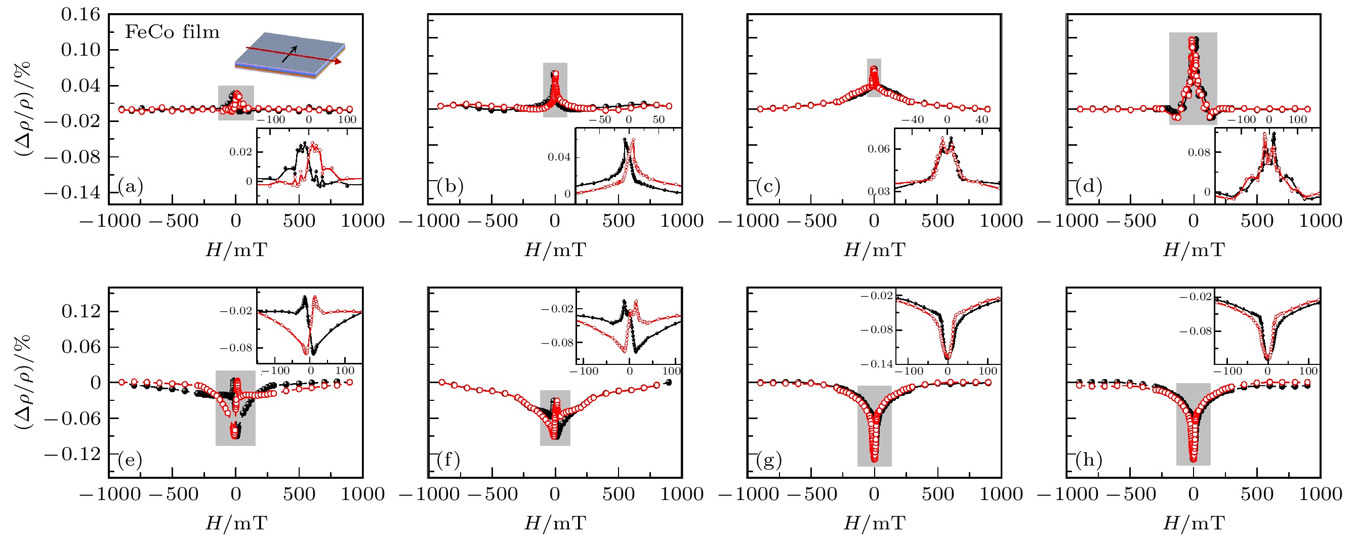
图 3 室温且I⊥H时, FeCo薄膜(a)和不同Cr厚度Gd (4 nm)/Cr (tCr)/FeCo (5 nm)薄膜(b)—(h)的MR随磁场的变化 (a) FeCo; (b) tCr = 0; (c) tCr = 1.0 nm; (d) tCr = 1.5 nm; (e) tCr = 2.0 nm; (f) tCr = 2.5 nm; (g) tCr = 3.0 nm; (h) tCr = 3.5 nm (图3(a)右上角插图表示电流方向垂直于磁场方向, 磁场沿着薄膜平面内; 实心点表示磁场下降的分支, 空心点表示磁场上升的分支; 其余插图均为对应阴影部分的放大图)
Fig. 3. Variation of MR with the magnetic field for (a) FeCo film and (b)–(h) Gd (4 nm)/Cr (tCr)/FeCo (5 nm) films with different thickness of Cr at the room temperature and I⊥H: (a) FeCo film; (b) tCr = 0; (c) tCr = 1.0 nm; (d) tCr = 1.5 nm; (e) tCr = 2.0 nm; (f) tCr = 2.5 nm; (g) tCr = 3.0 nm; (h) tCr = 3.5 nm (The current direction is perpendicular to the direction of magnetic field, and the magnetic field is along the in-plane of the film, as shown in top-right of Fig. 3(a). Solid dots indicate downwards branches, open dots indicate upwards branches. The other insets are the enlarged images of the corresponding shaded parts).
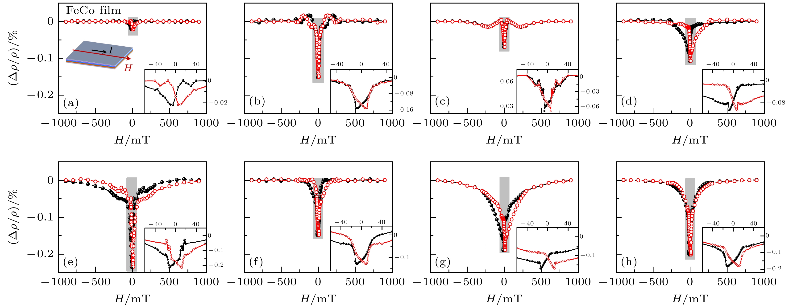
图 4 室温且I//H时, FeCo薄膜(a)和不同Cr厚度Gd (4 nm)/Cr (tCr)/FeCo (5 nm)薄膜(b)—(h)的MR随磁场的变化 (a) FeCo; (b) tCr = 0; (c) tCr = 1.0 nm; (d) tCr = 1.5 nm; (e) tCr = 2.0 nm; (f) tCr = 2.5 nm; (g) tCr = 3.0 nm; (h) tCr = 3.5 nm (图4(a)左边插图表示电流方向平行于磁场方向, 磁场沿着薄膜平面内; 实心点表示磁场下降的分支, 空心点表示磁场上升的分支; 其余插入图均为对应阴影部分的放大图)
Fig. 4. Variation of MR with the magnetic field for (a) FeCo film and (b)–(h) Gd (4 nm)/Cr (tCr)/FeCo (5 nm) films with different thickness of Cr at the room temperature and I//H: (a) FeCo film; (b) tCr = 0; (c) tCr = 1.0 nm; (d) tCr = 1.5 nm; (e) tCr = 2.0 nm; (f) tCr = 2.5 nm; (g) tCr = 3.0 nm; (h) tCr = 3.5 nm (With current parallel to H, and the magnetic field is along the in-plane of the film, as illustrated the inset in the left of Fig. 4(a). Solid dots indicate downwards branches, open dots indicate upwards branches. The other insets are the enlarged images of the corresponding shaded parts).
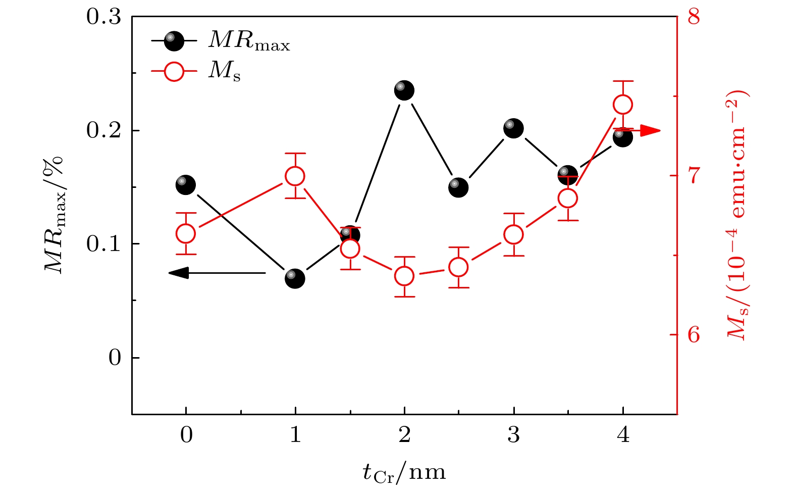
图 5 室温下电流方向平行于磁场方向时, MR最大值(MRmax)和薄膜单位面积饱和磁化强度(Ms)与Cr层厚度的变化关系
Fig. 5. Relationship of the maximum magnetoresistance (MRmax) with the configuration of current parallel to the magnetic field and saturation magnetization per unit area (Ms) to the film and the thickness of the Cr layer at room temperature.
图 6 5 K时, FeCo薄膜(a)和不同Cr厚度Gd (4 nm)/Cr (tCr)/FeCo (5 nm) 薄膜(b)—(h)的面内磁滞回线 (a) FeCo薄膜; (b) tCr = 0; (c) tCr = 1.0 nm; (d) tCr = 1.5 nm; (e) tCr = 2.0 nm; (f) tCr = 2.5 nm; (g) tCr = 3.0 nm; (h) tCr = 4.0 nm (虚线矩形方框是具有Cr中间层薄膜的磁滞回线中矩形度较好的部分)
Fig. 6. In-plane magnetization hysteresis loops for (a) FeCo film and (b)–(h) Gd (4 nm)/Cr(tCr)/FeCo (5 nm) films with different thickness of 5 K: (a) FeCo film; (b) tCr = 0; (c) tCr = 1.0 nm; (d) tCr = 1.5 nm; (e) tCr = 2.0 nm; (f) tCr = 2.5 nm; (g) tCr = 3.0 nm; (h) tCr = 4.0 nm (The easy magnetized parts are marked by rectangles in the hysteresis loop for films with Cr spacer layer).
表 1 不同 Cr 层厚度的Gd/Cr/FeCo薄膜在5 K下的单位面积饱和磁化强度(MsLT)、 5 K下磁滞回线中间矩形度较好部分的磁矩(见图6矩形)占总薄膜磁矩的比例(R)、R部分的磁矩(MFeCo)、磁滞回线中缓慢磁化部分对应的磁矩(M)
Table 1. Saturation magnetization per area at 5 K (MsLT) for Gd/Cr/FeCo films with different thickness of Cr layer (tCr), the percentage (R) of the magnetic moment in the middle of the hysteresis loop with better squareness (represented by the rectangles in Fig. 6) to the total magnetic moment at 5 K, the magnetic moment (MFeCo) of R, and the magnetic moment (M) in the slowly magnetized part of the hysteresis loop.
tCr/nm MsLT/(10–4 emu·cm–2) R MFeCo/(10–4 emu·cm–2) M/(10–4 emu·cm–2) 0 7.52 ± 0.75 — — — 1.0 11.30 ± 1.13 0.69 7.78 ± 0.78 4.02 ± 0.40 1.5 11.65 ± 0.12 0.65 7.60 ± 0.76 4.37 ± 0.44 2.0 15.30 ± 0.15 0.48 7.29 ± 0.73 8.02 ± 0.80 2.5 17.03 ± 1.70 0.46 7.78 ± 0.78 9.75 ± 0.98 3.0 10.87 ± 1.09 0.68 7.35 ± 0.74 3.59 ± 0.36 4.0 10.56 ± 1.06 0.64 6.73 ± 0.67 3.28 ± 0.33 -
[1] Lee J C T, Chess J J, Montoya S A, Shi X, Tamura N, Mishra S K, Fischer P, McMorran B J, Sinha S K, Fullerton E E, Kevan S D, Roy S 2016 Appl. Phys. Lett. 109 022402
 Google Scholar
[2] Talapatra A, Chelvane J A, Satpati B, Kumar S, Mohanty J 2019 J. Alloy. Compd. 774 1059
 Google Scholar
[3] Bhatt R C, Liao C M, Ye L X, Hai N T, Wu J C, Wu T H 2021 J. Magn. Magn. Mater. 526 167734
 Google Scholar
[4] Inyang O, Rafiq A, Swindells C, Ali S, Atkinson D 2020 Sci. Rep. 10 9767
 Google Scholar
[5] Kirk E, Bull C, Finizio S, et al. 2020 Phys. Rev. Mater. 4 074403
 Google Scholar
[6] Huang M, Qiu Z, Wang F, Luo H, Zhang J 2022 J. Alloy. Compd. 901 163619
 Google Scholar
[7] Ming X, Han X, Yang M, Yan G 2022 J. Magn. Magn. Mater. 550 169064
 Google Scholar
[8] Jin H M 1983 J. Magn. Magn. Mater. 35 283
 Google Scholar
[9] Elhamali S M, Ibrahim N B, Radiman S 2018 Mater. Chem. Phys. 208 1
 Google Scholar
[10] Talapatra, Chelvane J A, Mohanty J 2021 J. Alloy. Compd. 861 157953
 Google Scholar
[11] Wang K, Tang Y, Zhang K, Wang Y, Liu J 2021 Mater. Sci. Eng. B-Adv. 263 114848
 Google Scholar
[12] Basumatary H, Chelvane J A, Rao D V S, Talapatra A, Mohanty J, Kumar D, Singh V, Kamat S V, Ranjan R 2021 J. Alloy. Compd. 869 159571
 Google Scholar
[13] Bhatt R C, Ye L X, Hai N T, Wu J C, Wu T H 2021 J. Magn. Magn. Mater. 537 168196
 Google Scholar
[14] Stanciu A E, Schinteie G, Kuncser A, Iacob N, Trupina L, Ionita I, Crisan O, Kuncser V 2020 J. Magn. Magn. Mater. 498 166173
 Google Scholar
[15] Morishita T, Togami Y, Tsushima K 1986 J. Magn. Magn. Mater. 54–57 789
 Google Scholar
[16] Frąckowiak Ł, Stobiecki F, Urbaniak M, Matczak M, Chaves-O`Flynn G D, Bilski M, Glenz A, Kuświk P 2022 J. Magn. Magn. Mater. 544 168682
 Google Scholar
[17] Wang J, Li C, Wang Y, Tang R, Chai G, Jiang C 2021 Appl. Surf. Sci. 567 150527
 Google Scholar
[18] Rebei A, Hohlfeld J 2006 Phys. Rev. Lett. 97 117601
 Google Scholar
[19] 高瑞鑫, 徐振, 陈达鑫, 徐初东, 陈志峰, 刘晓东, 周仕明, 赖天树 2009 物理学报 58 580
 Google Scholar
Gao R X, Xu Z, Chen D X, Xu C D, Chen Z F, Liu X D, Zhou S M, Lai T S 2009 Acta Phys. Sin. 58 580
 Google Scholar
[20] Sun L, Yue J J, Jiang S, Xu Y J, Li Q N, Chen Q, Zhou X C, Huang Z C, Yao Z Y, Zhai Y, Zhai H R 2017 J. Alloy. Compd. 695 1324
 Google Scholar
[21] Guo H S, Li L Z, Wu X H, Zhong Z C, Tao Z X, Wang F H, Wang T 2021 J. Magn. Magn. Mater. 538 168249
 Google Scholar
[22] Ceballos A, Pattabi A, El-Ghazaly A, Ruta S, Simon C P, Evans R F L, Ostler T, Chantrell R W, Kennedy E, Scott M, Bokor J, Hellman F 2021 Phys. Rev. B 103 024438
 Google Scholar
[23] 侯育花, 黄有林, 刘仲武, 曾德长 2015 物理学报 64 037501
 Google Scholar
Hou Y H, Huang Y L, Liu Z W, Zeng D C 2015 Acta Phys. Sin. 64 037501
 Google Scholar
[24] Hao A, Ismail M, He S, Qin N, Chen R, Rana A M, Bao D 2018 Mater. Sci. Eng. B-Adv. 229 86
 Google Scholar
[25] Chakrabarty S, Sinha A, Dutta A, Pal M 2018 J. Magn. Magn. Mater. 468 215
 Google Scholar
[26] Bulai G, Trandafir V, Irimiciuc S A, Ursu L, Focsa C, Gurlui S 2019 Ceram. Int. 45 20165
 Google Scholar
[27] Bohr C, Yu P, Scigaj M, Hegemann C, Fischer T, Coll M, Mathur S 2020 Thin Solid Films 698 137848
 Google Scholar
[28] Sharma S, Verma M K, Sharma N D, Choudhary N, Singh S, Singh D 2021 Ceram. Int. 47 17510
 Google Scholar
[29] Li N, Tang J, Su L, Ke Y J, Zhang W, Xie Z K, Sun R, Zhang X Q, He W, Cheng Z H 2021 Chin. Phys. B 30 117502
 Google Scholar
[30] Shan Z S, Sellmyer D J 1990 Phys. Rev. B 42 10433
 Google Scholar
[31] Kim W S, Andrä W, Kleemann W 1998 Phys. Rev. B 58 6346
 Google Scholar
[32] Schmidt T, Hoffmann H 2002 J. Magn. Magn. Mater. 248 181
 Google Scholar
[33] Drovosekov A B, Savitsky A O, Kholin D I, Kreines N M, Proglyado V V, Makarova M V, Kravtsov E A, Ustinov V V 2019 J. Magn. Magn. Mater. 475 668
 Google Scholar
[34] Xiang O, Xiong C, Wang Z, Zhang Y, Xu Y, Yi L, Piao H G, Pan L 2020 J. Magn. Magn. Mater. 516 167334
 Google Scholar
[35] Basha M A, Prajapat C L, Bhatt H, Kumar Y, Gupta M, Kinane C J, Cooper J F K, Langridge S, Basu S, Singh S 2020 J. Magn. Magn. Mater. 516 167331
 Google Scholar
[36] Mattson J E, Sowers C H, Berger A, Bader S D 1992 Phys Rev Lett. 68 3252
 Google Scholar
[37] Bellouard C, George B, Marchal G, Maloufi N, Eugène J 1997 J. Magn. Magn. Mater. 165 312
 Google Scholar
[38] Sun L, Li X Y, Zhao X C, Ban D M, Li G J, Yao Z H, Zhao Z B, Zhai Y, Cui X Y 2021 J Mater Sci: Mater Electron 32 28245
 Google Scholar
[39] George J M, Pereira L G, Barthélémy A, Petroff F, Steren L, Duvail J L, Fert A, Loloee R, Holody P, Schroeder P A 1994 Phys. Rev. Lett. 72 408
 Google Scholar
[40] Renard J P, Bruno P, Mégy R, Bartenlian B, Beauvillain P, Chappert C, Dupas C, Kolb E, Mulloy M, Veillet P, Vélu E 1995 Phys. Rev. B 51 12821
 Google Scholar
[41] Sanyal B, Antoniak C, Burkert T, Krumme B, Warland A, Stromberg F, Praetorius C, Fauth K, Wende H, Eriksson O 2010 Phys. Rev. Lett. 104 156402
 Google Scholar
[42] Scheunert G, Hendren W R, Ward C, Bowman R M 2012 App. Phys. Lett. 101 142407
 Google Scholar
[43] Liu Y F, Cai J W, Sun L 2010 Appl. Phys. Lett. 96 092509
 Google Scholar
[44] Jiao Z, Chen H, Jiang W, Wang J, Zhou Y, Yu S, Hou Y, Ye Q 2015 Mater. Lett. 158 241
 Google Scholar
[45] Zhao W, Liu C, Huang W, Hou C, Chen Z, Luo Z, Yin Y, Li X 2019 Mater. Lett. 240 124
 Google Scholar
[46] Peng C, Chen D, Dai D 1993 Solid State Commun. 87 161
 Google Scholar
[47] Parkin S S P, More N, Roche K P 1990 Phys, Rev. Lett. 64 2304
 Google Scholar
[48] Parkin S S P, Bhadra R, Roche K P 1991 Phys. Rev. Lett. 66 2152
 Google Scholar
计量
- 文章访问数: 6850
- PDF下载量: 70
- 被引次数: 0


 下载:
下载:
