-
黑体辐射通常具有覆盖整个红外波长范围的宽带光谱, 导致红外波段的大部分能量不能有效利用, 降低了辐射效率. 近年来, 具有二维亚波长人工纳米结构的超构表面因其在调节光学特性方面的灵活性而得到广泛研究, 这为调控热辐射提供了一个理想的平台. 在超构表面中, 采用合成维度方法为热辐射的精细调控开辟了新路径, 尤其突显了超越传统三维体系的物理特性和丰富的拓扑物理. 相比于在三维系统中探索物理现象, 研究一维或二维系统更为可行和高效. 合成维度的方法通过引入系统的结构或物理参数, 为操控光子系统中的内在自由度提供了可能性. 本文研究了利用合成维度方法实现波长选择热辐射. 首先在超晶格模型中构建合成拓扑外尔点, 通过角分辨热辐射谱(ARTES)对合成外尔锥进行实验表征, 在实现了合理的波长选择热辐射的同时能够尽可能地抑制其他波长的辐射, 对于实际的红外应用, 如热光伏和热管理装置, 是必不可少的.Blackbody emission such as the emission from incandescent sources usually possesses a broadband emission spectrum covering the whole infrared wavelength range. Most of emission energy goes into the unwanted infrared range and consequently causes low emission efficiency. Recently, metasurfaces with two-dimensional subwavelength artificial nanostructures have been widely studied due to their flexibility in modulating optical properties, thus providing an ideal platform for controlling thermal emission. The use of synthetic dimension methods in metasurfaces has opened up new avenues for fine-tuning thermal emission, especially highlighting the physical properties beyond traditional three-dimensional systems and rich topological physics. Although it is theoretically possible to explore physical phenomena through complete three-dimensional structures, such structures are difficult to construct in practice. In contrast, studying one-dimensional system or two-dimensional system is more feasible and efficient. The synthetic dimension approach introduces the possibility of manipulating intrinsic degrees of freedom in photon systems by introducing structural or physical parameters. In this work, we propose utilizing synthetic dimension methods to achieve wavelength-selective thermal emission. Firstly, we construct synthetic Weyl point in a superlattice model and validate it theoretically. Subsequently, experimental characterization of synthetic Weyl cones is conducted by using angle-resolved thermal emission spectroscopy (ARTES). The experimental results demonstrate that we can achieve reasonable wavelength-selective thermal emission while suppressing emission at other wavelengths as much as possible. This is essential for practical infrared applications such as thermalphotovoltaics and thermal management devices.
-
Keywords:
- thermal emission /
- metasurfaces /
- superlattices /
- synthetic dimensions
[1] Chu Q Q, Zhong F, Shang X H, Zhang Y, Zhu S N, Liu H 2024 Nanophotonics 13 1279
 Google Scholar
[2] Li A B, Singh S, Sievenpiper D 2018 Nanophotonics 7 989
 Google Scholar
[3] Chen H T, Taylor A J, Yu N F 2016 Rep. Prog. Phys. 79 076401
 Google Scholar
[4] Diem M, Koschny T, Soukoulis C M 2009 Phys. Rev. B 79 033101
 Google Scholar
[5] Doiron C F, Naik G V 2019 Adv. Mater. 31 1904154
 Google Scholar
[6] Zhang X, Liu H, Zhang Z G, Wang Q, Zhu S N 2017 Sci. Rep. 7 41858
 Google Scholar
[7] Zhang X, Zhang Z G, Wang Q, Zhu S N, Liu H 2019 ACS Photonics 6 2671
 Google Scholar
[8] Chu Q Q, Zhang F Y, Zhang Y, Qiao T, Zhu S N, Liu H 2022 Nanophotonics 11 4263
 Google Scholar
[9] Chu Q Q, Zhang F Y, Zhang Y, Zhu S N, Liu H 2023 Opt. Express 31 39832
 Google Scholar
[10] Zhong F, Zhang Y, Zhu S N, Liu H 2021 Opt. Express 29 35216
 Google Scholar
[11] Makhsiyan M, Bouchon P, Jaeck J, Pelouard J L, Haïder R 2015 Appl. Phys. Lett. 107 251103
 Google Scholar
[12] Li J Y, Yu B W, Shen S 2020 Phys. Rev. Lett. 124 137401
 Google Scholar
[13] Kudyshev Z A, Kildishev A V, Shalaev V M, Boltasseva A 2020 Appl. Phys. Rev. 7 021407
 Google Scholar
[14] Streyer W, Feng K, Zhong Y, Hoffman A J, Wasserman D 2015 Appl. Phys. Lett. 107 081105
 Google Scholar
[15] Argyropoulos C, Le K Q, Mattiucci N, D'Aguanno G, Alù A 2013 Phys. Rev. B 87 205112
 Google Scholar
[16] Kong A, Cai B Y, Shi P, Yuan X C 2019 Opt. Express 27 30102
 Google Scholar
[17] Liu G Q, Liu X S, Chen J, Li Y Y, Shi L L, Fu G L, Liu Z Q 2019 Sol. Energy Mater. Sol. Cells 190 20
 Google Scholar
[18] Chen C, Liu Y H, Jiang Z Y, Shen C, Zhang Y, Zhong F, Chen L S, Zhu S N, Liu H 2022 Opt. Express 30 13391
 Google Scholar
[19] Xu C L, Qu S B, Pang Y Q, Wang J F, Yan M B, Zhang J Q, Wang Z L, Wang W J 2018 Infrared Phys. Technol. 88 133
 Google Scholar
[20] Zhou J R, Zhan Z G, Zhu F D, Han Y G 2023 ACS Appl. Mater. Interfaces 15 21629
 Google Scholar
[21] Zhu Y, Hou G Z, Wang Q Y, Zhu T, Sun T, Xu J, Chen K J 2022 Nanoscale 14 10816
 Google Scholar
[22] Zou C J, Ren G H, Hossain M M, et al. 2017 Adv. Opt. Mater. 5 1700460
 Google Scholar
[23] Yuan L Q, Lin Q, Xiao M, Fan S H 2018 Optica 5 1396
 Google Scholar
[24] Liu H, Yan Z W, Xiao M, Zhu S N 2021 Acta Opt. Sin. 41 0123002
 Google Scholar
[25] Zhang S C, Hu J P 2001 Science 294 823
 Google Scholar
[26] Qi X L, Hughes T L, Zhang S C 2010 Phys. Rev. B 81 159901
 Google Scholar
[27] Ozawa T, Price H M, Amo A, Goldman N, Hafezi M, Lu L, Rechtsman M C, Schuster D, Simon J, Zilberberg O, Carusotto I 2019 Rev. Mod. Phys. 91 015006
 Google Scholar
[28] Tang G J, He X T, Shi F L, Liu J W, Chen X D, Dong J W 2022 Laser Photon. Rev. 16 2100300
 Google Scholar
[29] Kraus Y E, Zilberberg O 2012 Phys. Rev. Lett. 109 116404
 Google Scholar
[30] Mei F, Zhu S L, Zhang Z M, Oh C H, Goldman N 2012 Phys. Rev. A 85 013638
 Google Scholar
[31] Tsomokos D I, Ashhab S, Nori F 2010 Phys. Rev. A 82 052311
 Google Scholar
[32] Yuan L Q, Fan S H 2016 Optica 3 1014
 Google Scholar
[33] Cheng D L, Lustig E, Wang K, Fan S H 2023 Light-Sci. Appl. 12 158
 Google Scholar
[34] Englebert N, Goldman N, Erkintalo M, Mostaan N, Gorza S P, Leo F, Fatome J 2023 Nat. Phys. 19 1014
 Google Scholar
[35] Wang B, Chen T, Zhang X D 2019 Annual Conference of Chinese-Society-of-Optical-Engineering(CSOE)-Quantum Information Technology (AOPC) Beijing, China, July 07–09, 2019
[36] Cardano F, D'Errico A, Dauphin A, Maffei M, Piccirillo B, de Lisio C, De Filippis G, Cataudella V, Santamato E, Marrucci L, Lewenstein M, Massignan P 2017 Nat. Commun. 8 15516
 Google Scholar
[37] Yang M, Zhang H Q, Liu Z H, Zhou Z W, Zhou X X, Xu J S, Han Y J, Li C F, Guo G C 2023 Sci. Adv. 9 eabp8943
 Google Scholar
[38] Bell B A, Wang K, Solntsev A S, Neshev D N, Sukhorukov A A, Eggleton B J 2017 Optica 4 1433
 Google Scholar
[39] Zhang F X, Feng Y M, Chen X F, Ge L, Wan W J 2020 Phys. Rev. Lett. 124 053901
 Google Scholar
[40] Liu J J, Li Z W, Chen Z G, Tang W Y, Chen A, Liang B, Ma G C, Cheng J C 2022 Phys. Rev. Lett. 129 084301
 Google Scholar
[41] Wang Q, Xiao M, Liu H, Zhu S N, Chan C T 2017 Phys. Rev. X 7 031032
[42] Yan Z W, Wang Q, Xiao M, Zhao Y L, Zhu S N, Liu H 2021 Phys. Rev. Lett. 127 013901
 Google Scholar
[43] Song W E, Wu S J, Chen C, Chen Y X, Huang C Y, Yuan L Q, Zhu S N, Li T 2023 Phys. Rev. Lett. 130 043803
 Google Scholar
[44] Fan X Y, Xia T Z, Qiu H H, Zhang Q C, Qiu C Y 2022 Phys. Rev. Lett. 128 216403
 Google Scholar
[45] Deng W M, Chen Z M, Li M Y, Guo C H, Tian Z T, Sun K X, Chen X D, Chen W J, Dong J W 2022 Light-Sci. Appl. 11 134
 Google Scholar
[46] Xia S, Lei S, Song D, Lauro L D, Alamgir I, Tang L, Xu J, Morandotti R, Buljan H, Chen Z J A P 2024 Adv. Photon. 6 026005
 Google Scholar
[47] Yang B, Guo Q H, Tremain B, Liu R J, Barr L E, Yan Q H, Gao W L, Liu H C, Xiang Y J, Chen J, Fang C, Hibbins A, Lu L, Zhang S 2018 Science 359 1013
 Google Scholar
[48] Wang Q, Ding K, Liu H, Zhu S N, Chan C T 2020 Opt. Express 28 1758
 Google Scholar
[49] Zhong F, Ding K, Zhang Y, Zhu S N, Chan C T, Liu H 2020 Phys. Rev. Appl. 13 014071
 Google Scholar
-
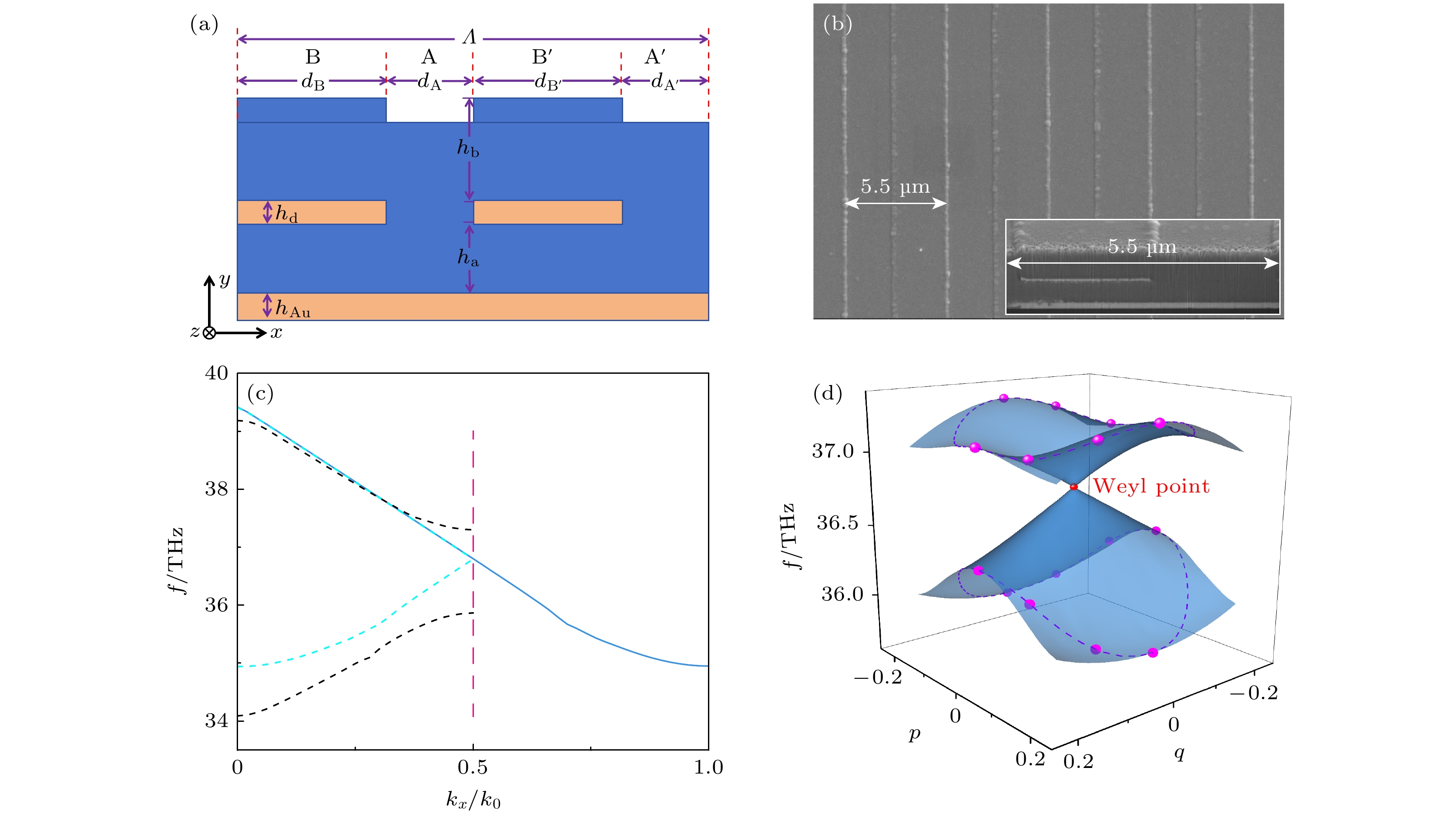
图 1 (a)超晶格的结构示意图; (b)参数为(p, q) = (0, 0)的实验样品对应的SEM扫描图; (c)不同参数下的超晶格色散, 红色虚线标出了超晶格的第一布里渊区边界, 蓝色实线和青色虚线代表参数设置为(p, q)=(0, 0)时的色散曲线, 青色虚线是由于人工加倍原胞周期而产生的能带折叠现象, 黑色虚线是参数(p, q) = (0, 0.2)对应的色散; (d)合成空间中的外尔锥, 紫色虚线是参数空间中对应$ {p}^{2}+{q}^{2}=0.{2}^{2} $的回路, 紫红色圆点是已表征的实验数据点
Fig. 1. (a) Schematic structure of the superlattice; (b) SEM picture corresponding to the experimental sample with the parameter (p, q) = (0, 0); (c) dispersion of the superlattice with different parameters, the red dashed line marks the boundary of the first Brillouin zone of the superlattice, the blue solid line and cyan dashed line represent the dispersion curves when the parameter is set to (p, q) = (0, 0), and the folding of the bands resulting from the artificial doubling of the unitcell period is marked by the cyan dashed line, and the black dashed line is the dispersion corresponding to the parameter (p, q) = (0, 0.2); (d) Weyl cones in the synthetic space, the purple dashed line is the loop in the parameter space corresponding to $ {p}^{2}+{q}^{2}=0.{2}^{2} $, and the fuchsia dots are the experimental data points that have been characterized.
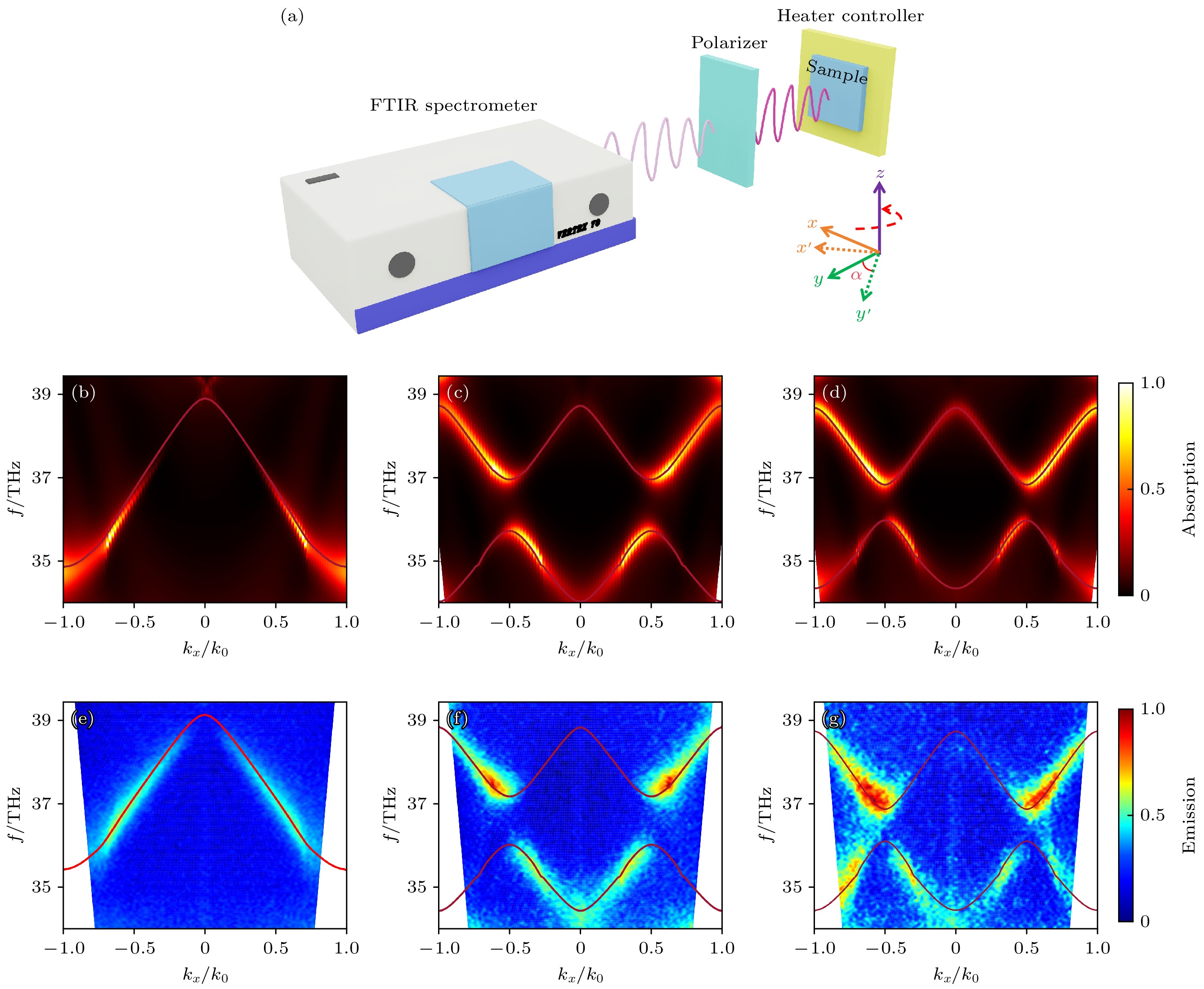
图 2 (a) ARTES测量装置及测量光路图; 由FDTD solutions计算的超晶格吸收谱(b)—(d)以及由ARTES测量的样品热辐射谱(e)—(g); (b), (e) 合成参数$ \left(p, q\right)=\left(0, 0\right) $; (c), (f)合成参数$ \theta =\pi /6 $; (d), (g) 合成参数$ \theta =\pi /3 $, 图片右边的颜色棒代表归一化吸收/辐射强度, 图中的暗红色实线来自COMSOL的仿真结果
Fig. 2. (a) ARTES measurement device and measurement optical path diagrams. The superlattice absorption spectra (b)–(d) calculated by FDTD and the thermal emission spectra (e)–(g) of the sample measured by ARTES: (b), (e) Correspond to the synthesis parameter (p, q) = (0, 0); (c), (f) correspond to the synthesis parameter θ = π/6; (d), (g) correspond to the synthesis parameter θ = π/3; colorbar on the right side of the picture represents the normalized absorbed/radiated intensity, and the dark red solid line in the diagram is from the COMSOL multiphysics simulation results.
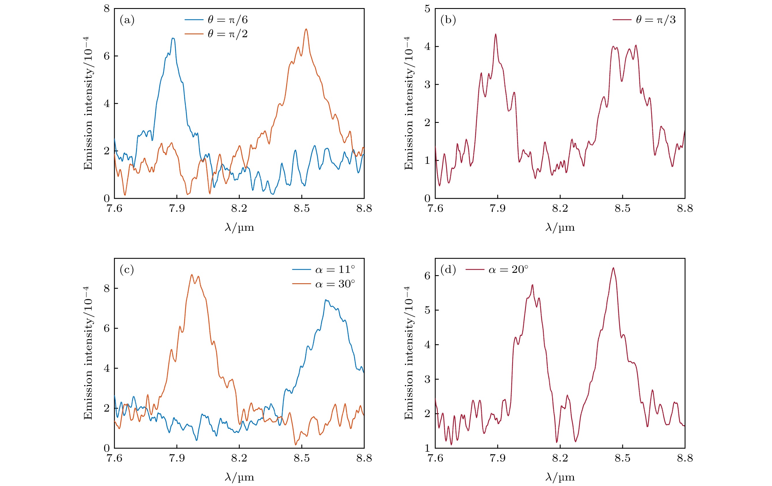
图 3 不同参数下的热辐射谱 (a)热辐射角$ \alpha =35^\circ $时, 不同$ \theta $角对应的热辐射谱; (b) 热辐射角$ \alpha =35^\circ $时, $ \theta ={\mathrm{\pi }}/3 $对应的热辐射谱; (c)热辐射角$ \theta ={\mathrm{\pi }}/6 $时, 不同$ \alpha $角对应的热辐射谱; (d) 热辐射角$ \theta ={\mathrm{\pi }}/6 $时, $ \alpha =20^\circ $对应的热辐射谱
Fig. 3. Thermal emission spectra with different parameters: (a) Thermal emission spectrum for different θ at thermal emission angle α = 35°; (b) thermal emission spectrum corresponding to θ = π/3 at thermal emission angle α = 35°; (c) thermal emission spectrum corresponding to θ = π/6 at different thermal emission angle α; (d) thermal emission spectrum corresponding to α = 20° for thermal emission angle θ = π/6
图 B1 合成角度θ = π/6, 当波矢为 (a) kx = 0.2k0, (b) kx = 0.4k0时高频率本征模式的模场分布以及当波矢为(c) kx = 0.2k0, (d) kx = 0.4k0时低频率本征模式的模场分布; (e) 合成角度θ = π/6时高频率色散对应的TE模式的远场辐射强度; (f) 合成角度θ = π/6时低频率色散对应的TE模式的远场辐射强度
Fig. B1. Mode-field distributions of the high-frequency eigenmodes at synthetic angle θ = π/6 when the wave vectors are (a) kx = 0.2k0, (b) kx = 0.4k0 and the low-frequency eigenmodes when the wave vectors are (c) kx = 0.2k0, (d) kx = 0.4k0; (e) the far-field radiation intensity of the TE modes corresponding to the high-frequency dispersion at synthetic angle θ = π/6; (f) the far-field radiation intensity of the TE mode corresponding to the low-frequency dispersion at synthetic angle θ = π/6.
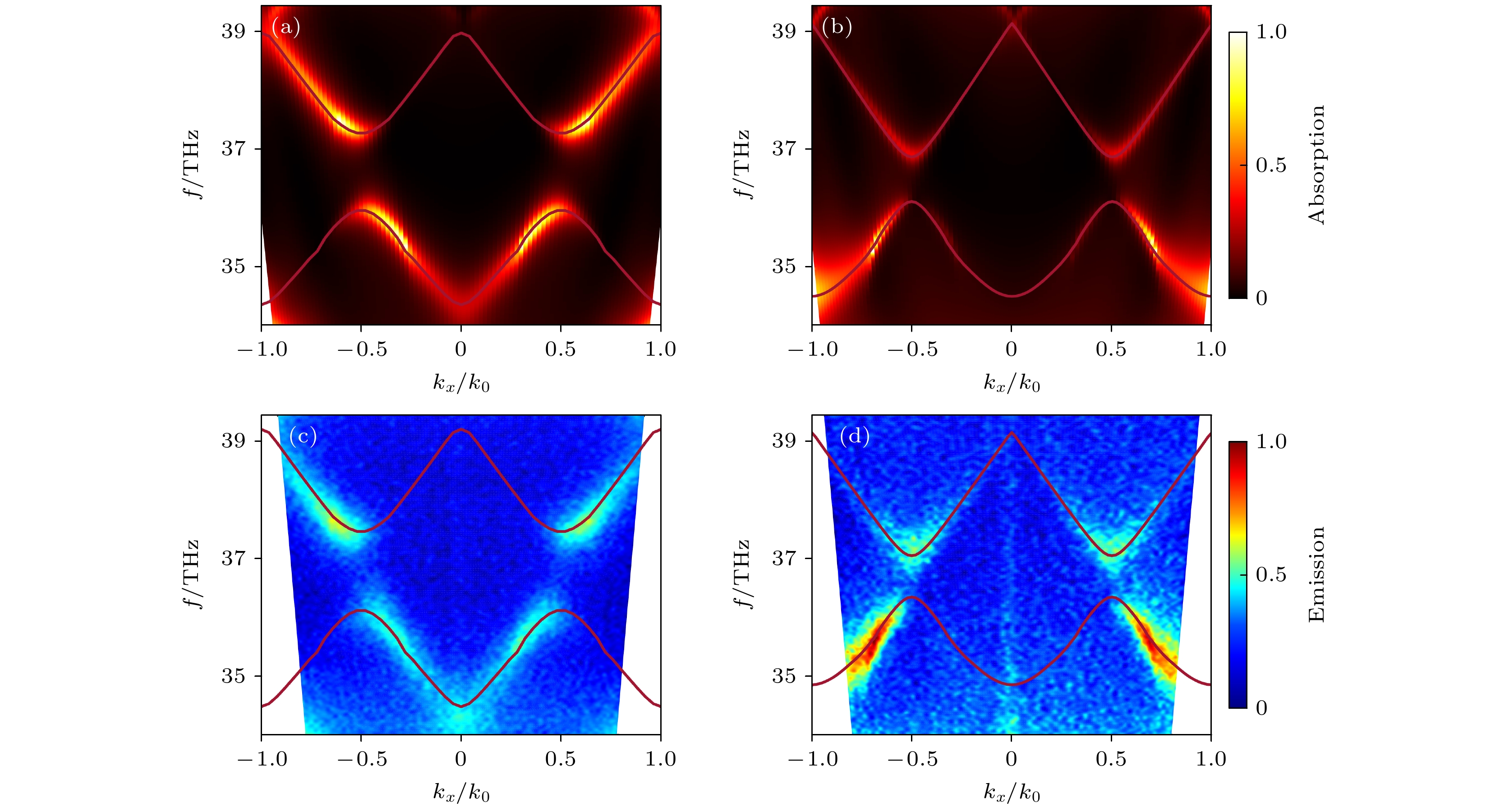
图 A1 由FDTD计算的超晶格吸收谱(a), (b)以及由ARTES测量的样品热辐射谱(c), (d); (a), (c) 合成参数$ \theta =0 $; (b), (d) 合成参数$ \theta ={\mathrm{\pi }}/2 $; 图片右边的颜色棒代表归一化吸收/辐射强度, 图中的暗红色实线来自COMSOL的仿真结果
Fig. A1. Superlattice absorption spectra (a), (b) calculated by FDTD and thermal emission spectra (c), (d) of the sample measured by ARTES: (a), (c) Synthesis parameter θ = 0; (b), (d) synthesis parameter θ = π/2; colorbar on the right side of the picture represents normalized absorption/emission intensity, and the dark-red solid line in the picture is from COMSOL simulation result.
-
[1] Chu Q Q, Zhong F, Shang X H, Zhang Y, Zhu S N, Liu H 2024 Nanophotonics 13 1279
 Google Scholar
[2] Li A B, Singh S, Sievenpiper D 2018 Nanophotonics 7 989
 Google Scholar
[3] Chen H T, Taylor A J, Yu N F 2016 Rep. Prog. Phys. 79 076401
 Google Scholar
[4] Diem M, Koschny T, Soukoulis C M 2009 Phys. Rev. B 79 033101
 Google Scholar
[5] Doiron C F, Naik G V 2019 Adv. Mater. 31 1904154
 Google Scholar
[6] Zhang X, Liu H, Zhang Z G, Wang Q, Zhu S N 2017 Sci. Rep. 7 41858
 Google Scholar
[7] Zhang X, Zhang Z G, Wang Q, Zhu S N, Liu H 2019 ACS Photonics 6 2671
 Google Scholar
[8] Chu Q Q, Zhang F Y, Zhang Y, Qiao T, Zhu S N, Liu H 2022 Nanophotonics 11 4263
 Google Scholar
[9] Chu Q Q, Zhang F Y, Zhang Y, Zhu S N, Liu H 2023 Opt. Express 31 39832
 Google Scholar
[10] Zhong F, Zhang Y, Zhu S N, Liu H 2021 Opt. Express 29 35216
 Google Scholar
[11] Makhsiyan M, Bouchon P, Jaeck J, Pelouard J L, Haïder R 2015 Appl. Phys. Lett. 107 251103
 Google Scholar
[12] Li J Y, Yu B W, Shen S 2020 Phys. Rev. Lett. 124 137401
 Google Scholar
[13] Kudyshev Z A, Kildishev A V, Shalaev V M, Boltasseva A 2020 Appl. Phys. Rev. 7 021407
 Google Scholar
[14] Streyer W, Feng K, Zhong Y, Hoffman A J, Wasserman D 2015 Appl. Phys. Lett. 107 081105
 Google Scholar
[15] Argyropoulos C, Le K Q, Mattiucci N, D'Aguanno G, Alù A 2013 Phys. Rev. B 87 205112
 Google Scholar
[16] Kong A, Cai B Y, Shi P, Yuan X C 2019 Opt. Express 27 30102
 Google Scholar
[17] Liu G Q, Liu X S, Chen J, Li Y Y, Shi L L, Fu G L, Liu Z Q 2019 Sol. Energy Mater. Sol. Cells 190 20
 Google Scholar
[18] Chen C, Liu Y H, Jiang Z Y, Shen C, Zhang Y, Zhong F, Chen L S, Zhu S N, Liu H 2022 Opt. Express 30 13391
 Google Scholar
[19] Xu C L, Qu S B, Pang Y Q, Wang J F, Yan M B, Zhang J Q, Wang Z L, Wang W J 2018 Infrared Phys. Technol. 88 133
 Google Scholar
[20] Zhou J R, Zhan Z G, Zhu F D, Han Y G 2023 ACS Appl. Mater. Interfaces 15 21629
 Google Scholar
[21] Zhu Y, Hou G Z, Wang Q Y, Zhu T, Sun T, Xu J, Chen K J 2022 Nanoscale 14 10816
 Google Scholar
[22] Zou C J, Ren G H, Hossain M M, et al. 2017 Adv. Opt. Mater. 5 1700460
 Google Scholar
[23] Yuan L Q, Lin Q, Xiao M, Fan S H 2018 Optica 5 1396
 Google Scholar
[24] Liu H, Yan Z W, Xiao M, Zhu S N 2021 Acta Opt. Sin. 41 0123002
 Google Scholar
[25] Zhang S C, Hu J P 2001 Science 294 823
 Google Scholar
[26] Qi X L, Hughes T L, Zhang S C 2010 Phys. Rev. B 81 159901
 Google Scholar
[27] Ozawa T, Price H M, Amo A, Goldman N, Hafezi M, Lu L, Rechtsman M C, Schuster D, Simon J, Zilberberg O, Carusotto I 2019 Rev. Mod. Phys. 91 015006
 Google Scholar
[28] Tang G J, He X T, Shi F L, Liu J W, Chen X D, Dong J W 2022 Laser Photon. Rev. 16 2100300
 Google Scholar
[29] Kraus Y E, Zilberberg O 2012 Phys. Rev. Lett. 109 116404
 Google Scholar
[30] Mei F, Zhu S L, Zhang Z M, Oh C H, Goldman N 2012 Phys. Rev. A 85 013638
 Google Scholar
[31] Tsomokos D I, Ashhab S, Nori F 2010 Phys. Rev. A 82 052311
 Google Scholar
[32] Yuan L Q, Fan S H 2016 Optica 3 1014
 Google Scholar
[33] Cheng D L, Lustig E, Wang K, Fan S H 2023 Light-Sci. Appl. 12 158
 Google Scholar
[34] Englebert N, Goldman N, Erkintalo M, Mostaan N, Gorza S P, Leo F, Fatome J 2023 Nat. Phys. 19 1014
 Google Scholar
[35] Wang B, Chen T, Zhang X D 2019 Annual Conference of Chinese-Society-of-Optical-Engineering(CSOE)-Quantum Information Technology (AOPC) Beijing, China, July 07–09, 2019
[36] Cardano F, D'Errico A, Dauphin A, Maffei M, Piccirillo B, de Lisio C, De Filippis G, Cataudella V, Santamato E, Marrucci L, Lewenstein M, Massignan P 2017 Nat. Commun. 8 15516
 Google Scholar
[37] Yang M, Zhang H Q, Liu Z H, Zhou Z W, Zhou X X, Xu J S, Han Y J, Li C F, Guo G C 2023 Sci. Adv. 9 eabp8943
 Google Scholar
[38] Bell B A, Wang K, Solntsev A S, Neshev D N, Sukhorukov A A, Eggleton B J 2017 Optica 4 1433
 Google Scholar
[39] Zhang F X, Feng Y M, Chen X F, Ge L, Wan W J 2020 Phys. Rev. Lett. 124 053901
 Google Scholar
[40] Liu J J, Li Z W, Chen Z G, Tang W Y, Chen A, Liang B, Ma G C, Cheng J C 2022 Phys. Rev. Lett. 129 084301
 Google Scholar
[41] Wang Q, Xiao M, Liu H, Zhu S N, Chan C T 2017 Phys. Rev. X 7 031032
[42] Yan Z W, Wang Q, Xiao M, Zhao Y L, Zhu S N, Liu H 2021 Phys. Rev. Lett. 127 013901
 Google Scholar
[43] Song W E, Wu S J, Chen C, Chen Y X, Huang C Y, Yuan L Q, Zhu S N, Li T 2023 Phys. Rev. Lett. 130 043803
 Google Scholar
[44] Fan X Y, Xia T Z, Qiu H H, Zhang Q C, Qiu C Y 2022 Phys. Rev. Lett. 128 216403
 Google Scholar
[45] Deng W M, Chen Z M, Li M Y, Guo C H, Tian Z T, Sun K X, Chen X D, Chen W J, Dong J W 2022 Light-Sci. Appl. 11 134
 Google Scholar
[46] Xia S, Lei S, Song D, Lauro L D, Alamgir I, Tang L, Xu J, Morandotti R, Buljan H, Chen Z J A P 2024 Adv. Photon. 6 026005
 Google Scholar
[47] Yang B, Guo Q H, Tremain B, Liu R J, Barr L E, Yan Q H, Gao W L, Liu H C, Xiang Y J, Chen J, Fang C, Hibbins A, Lu L, Zhang S 2018 Science 359 1013
 Google Scholar
[48] Wang Q, Ding K, Liu H, Zhu S N, Chan C T 2020 Opt. Express 28 1758
 Google Scholar
[49] Zhong F, Ding K, Zhang Y, Zhu S N, Chan C T, Liu H 2020 Phys. Rev. Appl. 13 014071
 Google Scholar
计量
- 文章访问数: 6003
- PDF下载量: 241
- 被引次数: 0


 下载:
下载:


