-
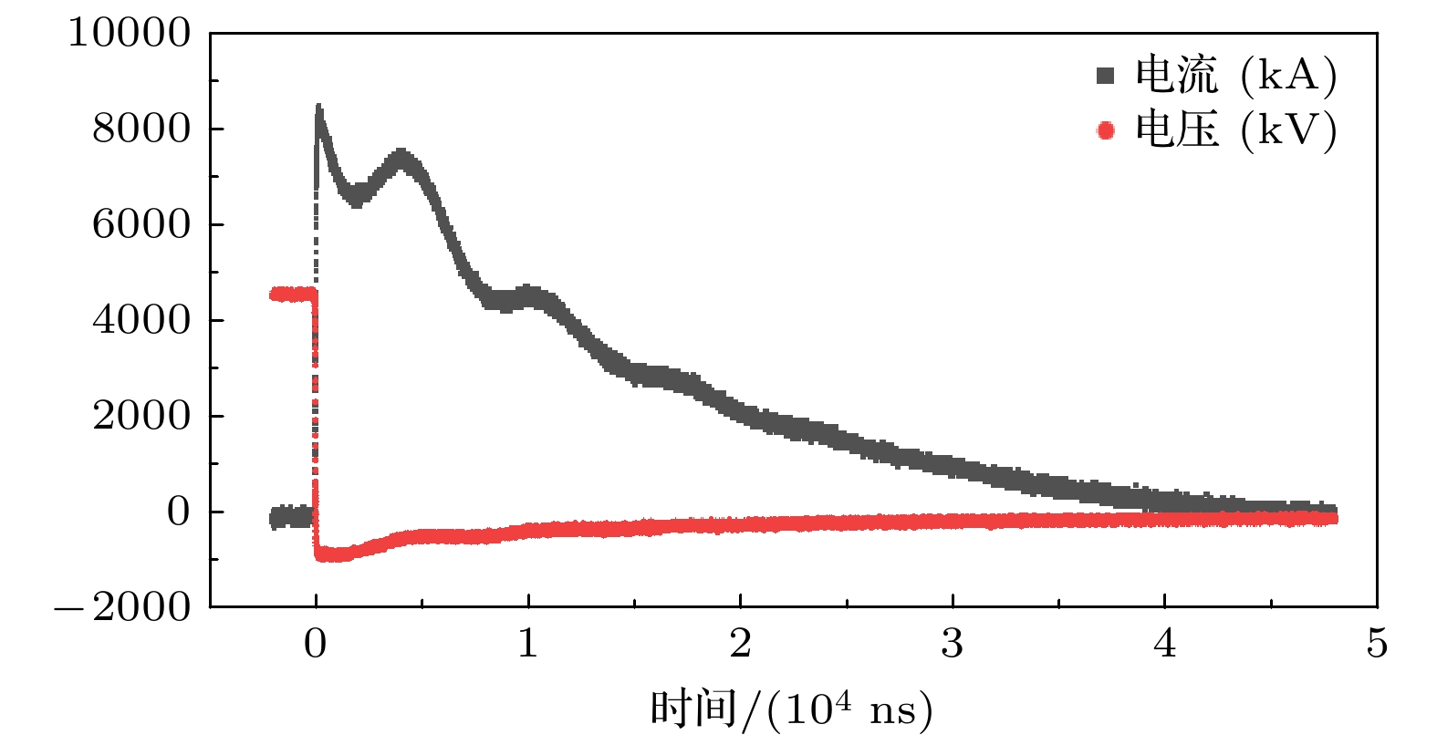
为了提升半导体开关的峰值功率与导通速度, 针对光控多门极晶闸管结构开展了系列实验研究, 重点探讨了不同光注入参数对开关特性的影响. 研究发现, 在不同激光峰值功率条件下, 开关芯片展现出不同的导通特性. 通过建立开关模型, 并对注入光参数及电路参数进行对比分析, 本工作提出了光控多门极晶闸管的3种工作模式设想: 光致线性模式(A模式)、场致非线性模式(C模式)和混合放大模式(B模式). 为验证这些工作模式, 我们进行了针对性的验证测试, 结果证实了该光控多门极晶闸管具有不同导通特性的工作模式. 开关多工作模式的发现与验证, 大幅度提升了功率半导体开关器件的导通速度(di/dt)水平和峰值功率. 在23 mm直径芯片上, A模式获得了4 kV, 8 kA, 440 kA/μs的窄脉冲; C模式获得了8.5 kV, 6.0 kA, 55 kA/μs的宽脉冲; 在38 mm直径芯片上, B模式获得了4.6 kV, 8.5 kA, 129 kA/μs的宽脉冲. 这些成果为超高峰值功率半导体开关组件的研发奠定了坚实的理论与实验基础.
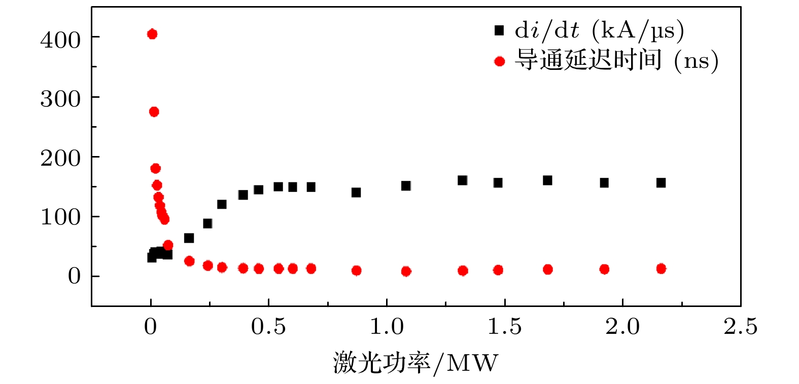
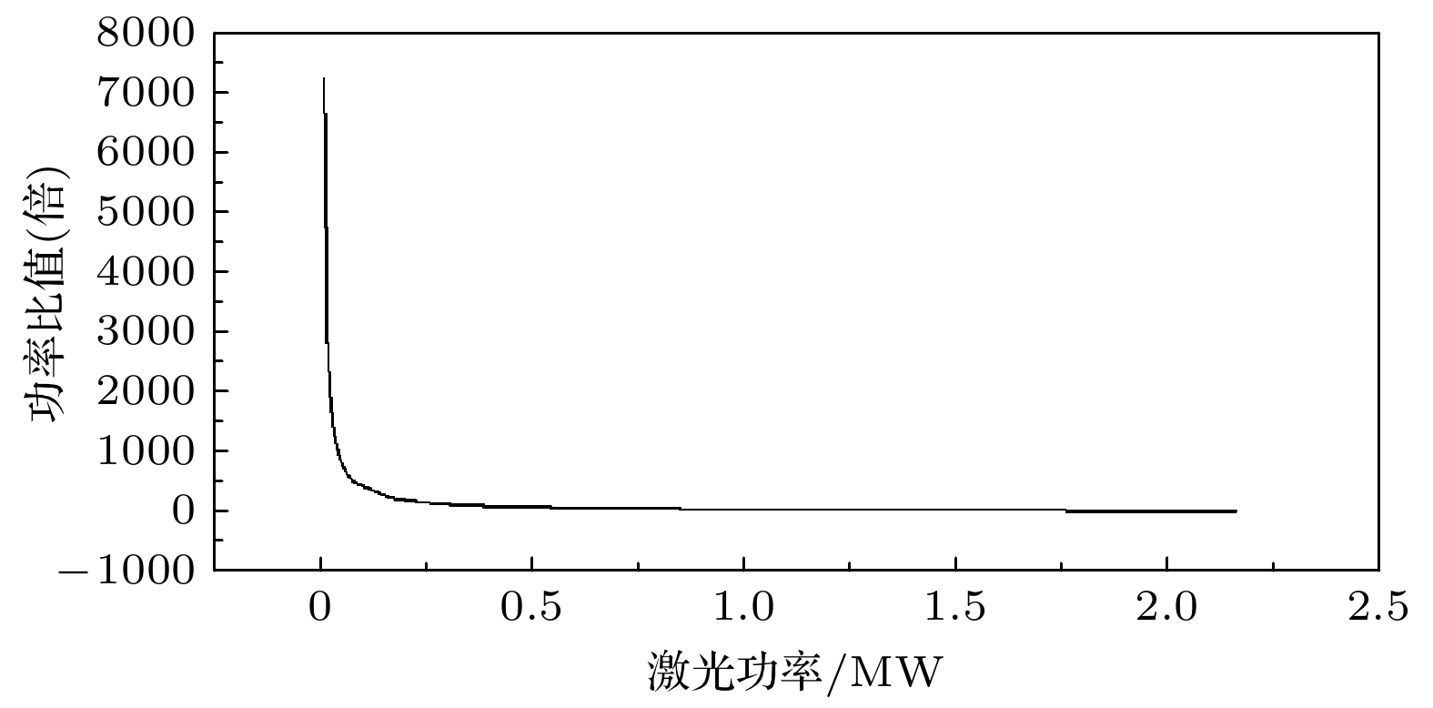
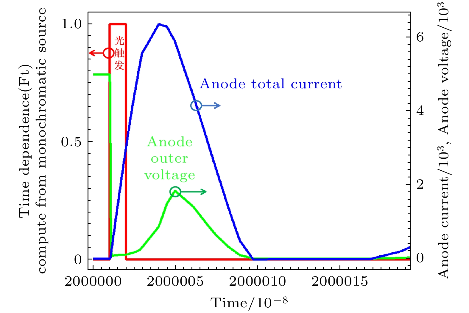
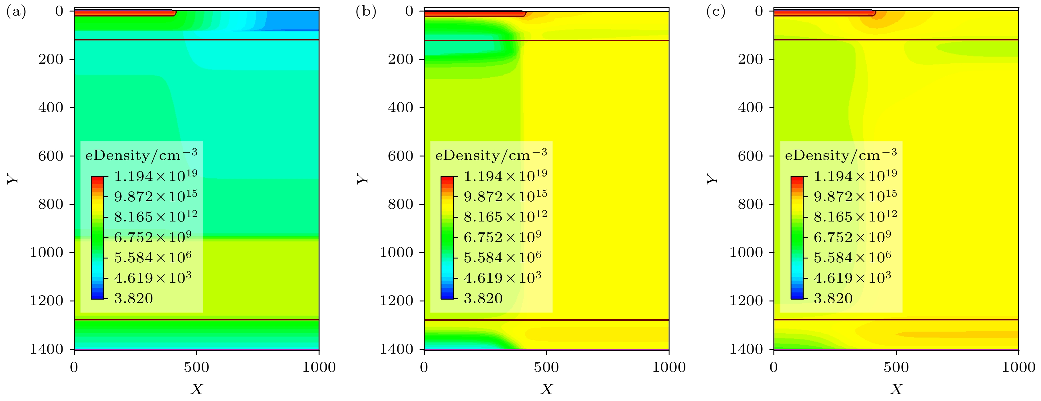
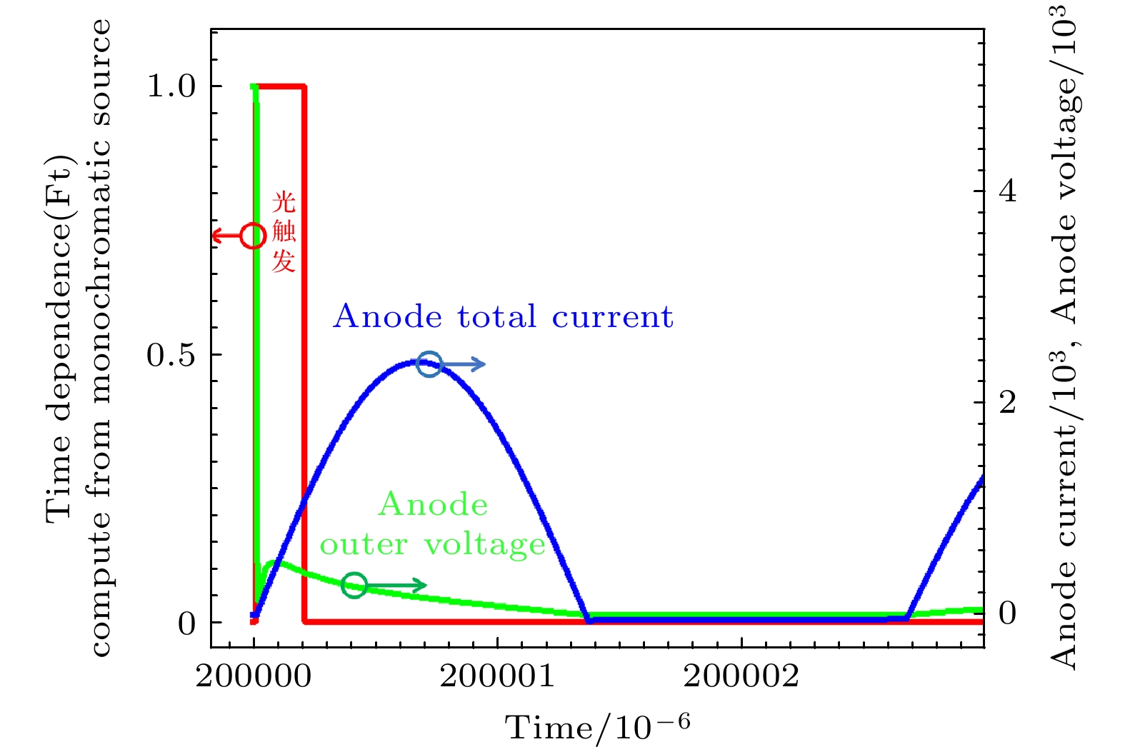
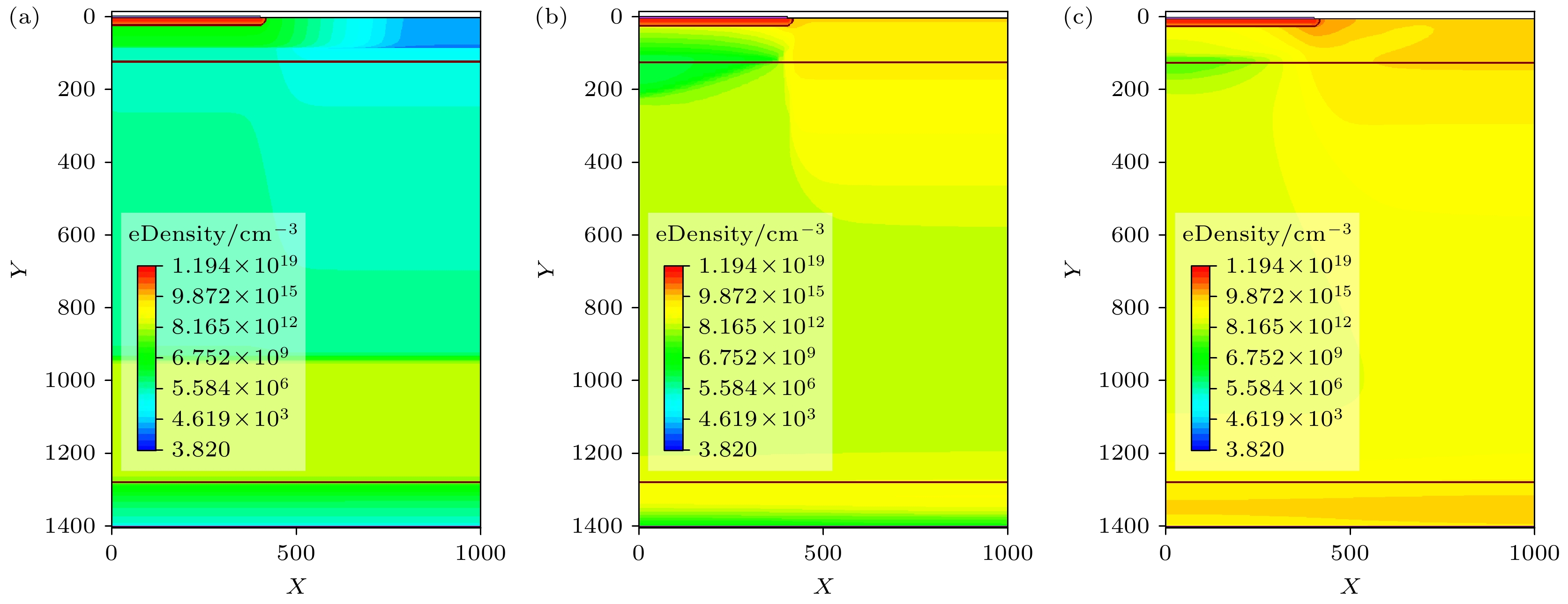
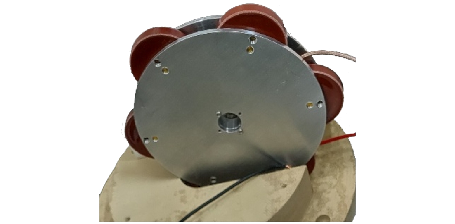
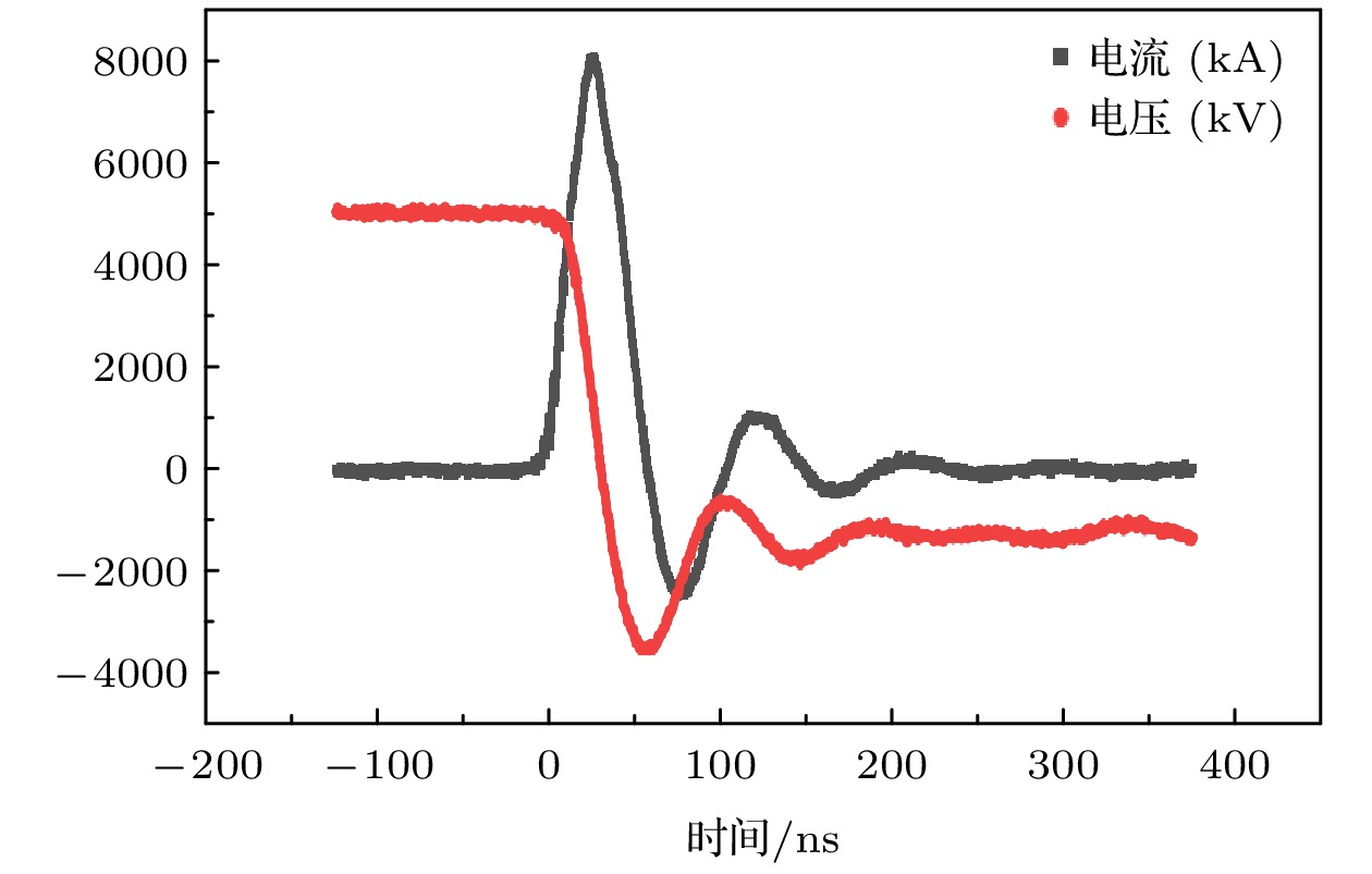
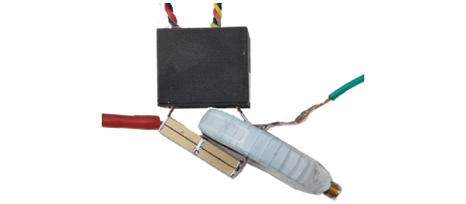
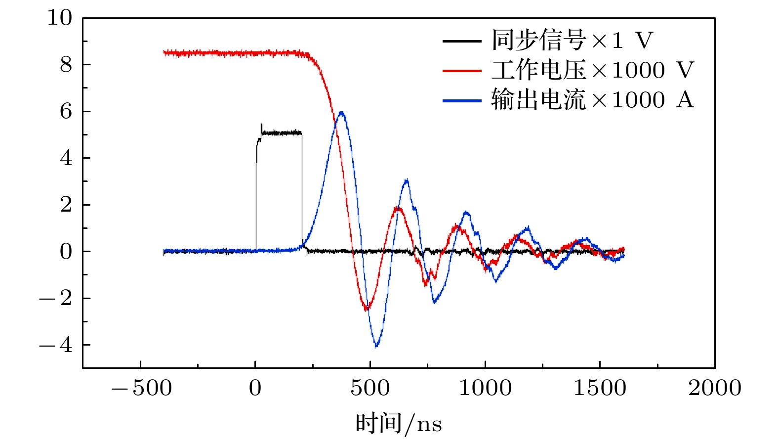
In order to meet the switching requirements of high-frequency pulsed-power systems and further enhance the peak power and turn-on speed of solid-state switches, comparative experiments on the structure of optically controlled multi-gate thyristors and the parameter of injected light are investigated in this work. The research results show that semiconductor chips based on the multi-gate thyristor structure exhibit different conduction characteristics under varying laser injection conditions, resulting in unique inflection point curves. By establishing a switching model and changing the injected light parameters and circuit parameter models, three conceptual operating modes for the optically controlled multi-gate thyristor are proposed, they being photonic linear mode (Mode A), field-induced nonlinear mode (Mode C), and hybrid amplification mode (Mode B). Based on these concepts, the experimental validation tests are conducted, and the three distinct operating characteristics of the optically controlled multi-gate thyristor are confirmed. In Mode A, the conduction process is mainly related to the injected light power parameters, which is similar to the scenario in the linear mode of traditional light-guided switches, thus Mode A is suitable for the narrow pulse width applications. Mode C mainly focuses on carrier multiplication after injection, resembling the conduction characteristics of super thyristors (SGTO), and this mode is suitable for wide pulse width and high current applications. In Mode B, its initial conduction is related to the injected light parameters, while the later carrier multiplication continues from the earlier photonic linear mode, achieving characteristics of both fast rise time and wide pulse width, effectively integrating the advantages of light-guided switches and SGTOs. In Mode A, when injected laser energy is 8.5 mJ, a pulse width is 10 ns, and peak power is 0.85 MW, the switch operates at a voltage of 5.2 kV, an output current of 8.1 kA, turn-on time (10%–90%) of 18.4 ns, with a di/dt value reaching 440 kA/μs. The main characteristic is that the di/dt of the switch is linearly related to the injected laser energy, thereby achieving a fast rise time output, which reflects the photonic linear conduction mode. This mode is suitable for high-power, narrow-pulse, and fast-rise-time applications, such as high-power microwave sources, and its characteristics are similar to those of gas switches. In Mode C, when triggering laser energy is set to 250 μJ, a pulse width is 210 ns, and peak power is 1200 W, the switch operates at a voltage of 8.5 kV, a short-circuit current of 6 kA and a current rise time of 110 ns, achieving a di/dt value exceeding 55 kA/μs. The key characteristic is that the di/dt of the switch is unrelated to the injected laser energy but is related to the electric field applied across the switch, thus it can operates at large current and wide pulse width, which reflects the field-induced nonlinear conduction mode. This mode is suitable for high-power, wide-pulse, and slower-rise-time applications, such as large current detonation and electromagnetic drives, and its characteristics are similar to those of igniter tubes and triggered light. In Mode B, when triggering laser energy is set to 10 mJ, a pulse width is 20 ns, and peak power is 0.5 MW, the switch operates at a voltage of 4.6 kV, with a short-circuit current reaching 8.5 kA and a current rise time of 66 ns, achieving a di/dt value exceeding 129 kA/μs. The main characteristic is that the initial conduction of the switch satisfies the photonic linear conduction mode, while the later conduction exhibits the field-induced nonlinear conduction mode, thus achieving both fast-rise-time output and the capability for large current and wide pulse width, reflecting a hybrid conduction mode. This mode is suitable for high-power and wide-pulse applications, such as accelerator power supplies, its characteristics are similar to those of hydrogen thyratrons and pseudo-spark switches. The discovery and validation of multiple operating modes for the switch significantly enhance the di/dt and peak power of power semiconductor switching devices, laying a theoretical and experimental foundation for the development of semiconductor switches with ultra-high peak power. Additionally, the switching devices are packaged according to their different operating modes and have been used in accelerator power supplies, solid-state detonators, and high-stability pulse drive sources, achieving positive results. -
Keywords:
- pulsed power /
- optically controlled switch /
- multi-mode /
- turn-on speed
[1] 刘锡三 2005 高功率脉冲技术(北京: 国防工业出版社) 第367页
Liu X S 2005 High Pulsed Power Technology (Beijing: National Defense Industry Press) p367
[2] 周前红, 董志伟, 简贵胄, 周海京 2015 物理学报 64 205206
 Google Scholar
Zhou Q H, Dong Z W, Jian G Z, Zhou H J 2015 Acta Phys. Sin. 64 205206
 Google Scholar
[3] 施卫, 田立强, 王馨梅, 徐鸣, 马德明, 周良骥, 刘宏伟, 谢卫平 2009 物理学报 58 1219
 Google Scholar
Shi W, Tian L Q, Wang X M, Xu M, Ma D M, Zhou L J, Liu H W, Xie W P 2009 Acta Phys. Sin. 58 1219
 Google Scholar
[4] 王公堂, 刘秀喜 2010 物理学报 59 1964
 Google Scholar
Wang G T, Liu X X 2010 Acta Phys. Sin. 59 1964
 Google Scholar
[5] Loquai S, Bölting M, Kellner U, Fischer J, Poisel H 2015 The 24th International Conference on Plastic Optical Fibers Nuremberg, Germany, September 22-24, 2015 p193
[6] 王凌云 2018 硕士学位论文(成都: 电子科技大学)
Wang L Y 2018 M. S. Dissertation (Chengdu: University of Electronic Science and Technology of China
[7] 王彩琳, 高勇, 马丽, 张昌利, 金垠东, 金相喆 2005 物理学报 54 2296
 Google Scholar
Wang C L, Gao Y, Ma L, Zhang C L, Kim E, Kim S 2005 Acta Phys. Sin. 54 2296
 Google Scholar
[8] Wang Y N, Ren L Y, Yang Z H, Shen S K, Deng Z C, Yuan Q, Ding W D, Ding Z J 2024 High Volt. 9 2
 Google Scholar
[9] 刘宾礼, 刘德志, 罗毅飞, 唐勇, 汪波 2013 物理学报 62 057202
 Google Scholar
Liu B L, Liu D Z, Luo Y F, Tang Y, Wang B 2013 Acta Phys. Sin. 62 057202
 Google Scholar
[10] Sanders H, Glidden S, Dunham C 2012 IEEE International Power Modulator and High Voltage Conference (IPMHVC) San Diego, CA, USA, June 3–7, 2012 p335
[11] Waldron J, Brandmier K 2017 IEEE International Conference on Plasma Science (ICOPS) Atlantic City, NJ, USA, May 21–25, 2017 p1
[12] Waldron J , Brandmier K , Temple V 2015 Pulsed Power Conference. IEEE Austin, Texas, USA, May 31–June 4, 2015 p7296986
[13] Chen W J, Liu C, Shi Y J, Liu Y W, Hong T, Liu C F, Zhou Q, Li Z J, Zhang B 2017 IEEE Trans. Electron Dev. 64 4206
 Google Scholar
[14] He D Z, Sun W J, Liao Y X, Zhang P H, Yu L, Dong S L, Yao C G, Liu X 2023 High Volt. 8 698
 Google Scholar
[15] M Junaid, Yu W Q, Cao S Z, Yu X L, Yu D S, Zong W L, Wang J H 2023 High Volt. 8 1275
 Google Scholar
[16] 袁雪林, 张洪德, 徐哲峰, 丁臻捷, 俞建国, 浩庆松, 曾搏, 胡龙 2010 固体电子学研究与进展 30 64
 Google Scholar
Yuan X L, Zhang H D, Xu Z F, Ding Z J, Yu J G, Hao Q S, Zeng B, Hu L 2010 Res. Prog. SSE 30 64
 Google Scholar
[17] Rukin S N 2020 Rev. Sci. Instrum. 91 011501
 Google Scholar
[18] 田立强, 潘璁, 施卫, 潘艺柯, 冉恩泽, 李存霞 2023 物理学报 72 178101
 Google Scholar
Tian L Q, Pan C, Shi W, Pan Y K, Ran E Z, Li C X 2023 Acta Phys. Sin. 72 178101
 Google Scholar
[19] 桂淮濛, 施卫 2018 物理学报 67 184207
 Google Scholar
Gui H M, Shi W 2018 Acta Phys. Sin. 67 184207
 Google Scholar
[20] 洪武, 梁琳, 余岳辉 2012 物理学报 61 058501
 Google Scholar
Hong W, Liang L, Yu Y H 2012 Acta Phys. Sin. 61 058501
 Google Scholar
[21] 米彦, 万佳仑, 卞昌浩, 姚陈果, 李成祥 2017 电工技术学报 32 244
Mi Y, Wan J L, Bian C H, Yao C G, Li C X 2017 Trans. China Electrotech. Soc. 32 244
[22] Rodin P, Ivanov M 2020 J. Appl. Phys. 127 044504
 Google Scholar
[23] 梁琳, 颜小雪, 黄鑫远, 卿正恒, 杨泽伟, 尚海 2022 中国电机工程学报 42 8631
Liang L, Yan X X, Huang X Y, Qing Z H, Yang Z W, Shang H 2022 Proc. CSEE 42 8631
[24] Lyublinsky A G, Korotkov S V, Aristov Y V, Korotkov D A 2013 IEEE Trans. Plasma Sci. 41 2625
 Google Scholar
[25] 王凌云, 刘宏伟, 袁建强, 谢卫平, 颜家圣 2024 电工技术学报 39 7566
Wang L Y, Liu H W, Yuan J Q, Xie W P, Yan J S 2024 Trans. China Electrotech. Soc. 39 7566
-
表 1 激光参数与开关典型参数实验数据表
Table 1. Experimental data table of laser parameters and typical switch parameters.
激光功率
/MW激光能量
/mJ充电电压
/kV电压下降
时间/ns电流峰值
/kA电流上升
时间/ns导通延迟
时间/ns电流脉冲
宽度/ns开关峰值
功率/MW功率
比值 Ndi/dt/
(kA·μs–1)2.16 21.6 4.5 44.3 10.54 67.2 13.5 652 47.4 22 157 1.92 19.2 4.5 44.6 10.54 67.3 12.6 654 47.4 25 157 1.68 16.8 4.5 45.4 10.48 65.3 12.1 665 47.2 28 160 1.47 14.7 4.5 45.4 10.42 66.4 11 667 46.9 32 157 1.32 13.2 4.5 46.3 10.34 64.3 10.1 661 46.5 35 161 1.08 10.8 4.5 48.6 10.35 68 8.88 663 46.6 43 152 0.87 8.7 4.5 50.2 10.07 71.6 10.2 684 45.3 52 141 0.678 6.78 4.5 46 9.71 65.1 13.7 742 43.7 64 149 0.6 6 4.5 47.4 9.71 65.1 13.5 742 43.7 73 149 0.54 5.4 4.5 52.5 9.41 62.7 13.5 765 42.3 78 150 0.46 4.6 4.5 60.3 9.17 63.3 13.4 795.6 41.3 90 145 0.39 3.9 4.5 68 8.62 63 14.1 832 38.8 99 137 0.3 3 4.5 128 8.52 70.5 15.4 829 38.3 128 121 0.24 2.4 4.5 158.4 8.48 95.8 18.6 835 38.2 159 89 0.162 1.62 4.5 196 8.39 130.4 25.9 842 37.8 233 64 0.072 0.72 4.5 221 8.13 222 52.6 857 36.6 508 37 0.057 0.57 4.5 254 8.23 199 96 848 37.0 650 41 0.0474 0.474 4.5 249.7 8.23 202 102 850 37.0 781 41 0.0438 0.438 4.5 263 8.22 197.8 108 869 37.0 845 42 0.0372 0.372 4.5 265 8.19 208.9 119 858 36.9 991 39 0.0312 0.312 4.5 278 8.17 218 133 852 36.8 1178 37 0.0252 0.252 4.5 252 8.16 212 153 874 36.7 1457 38 0.0186 0.186 4.5 251 8.13 203 181 878 36.6 1967 40 0.0126 0.126 4.5 271 7.97 212 276 897 35.9 2846 38 0.0048 0.048 4.5 351 7.78 245 406 955 35.0 7294 32 表 2 器件驱动激光能量、短路电流、开通前沿的关系
Table 2. The relationship between device drive laser energy, short-circuit current, and turn-on edge.
激光
能量/mJ工作
电压/kV短路
电流/kA电流
前沿/ns电流
脉宽/nsdi/dt
/(kA·μs–1)0.9 4 1.88 66.8 75.0 28 2.1 4 3.42 40 49.0 86 2.6 4 3.75 36.6 46.0 102 3.6 4 5.65 20.4 36.7 277 4.6 4 5.84 18.8 36.0 311 5.4 4 6.48 18.9 38.0 343 6.3 4 7 18.7 37.7 374 7.4 4 7.3 18.6 38.7 392 8.5 4 7.91 18.6 38.3 425 表 3 不同电压下开关的导通特性
Table 3. The conduction characteristics of the switch at different voltages.
激光
能量/μJ工作
电压
/kV短路
电流/kA电流
前沿
/nsdi/dt
/
(kA·μs–1)200 5.0 2.0 128 16 200 6.0 2.8 121 23 200 7.0 3.9 118 33 200 8.0 5.4 111 49 200 8.5 6.0 110 55 -
[1] 刘锡三 2005 高功率脉冲技术(北京: 国防工业出版社) 第367页
Liu X S 2005 High Pulsed Power Technology (Beijing: National Defense Industry Press) p367
[2] 周前红, 董志伟, 简贵胄, 周海京 2015 物理学报 64 205206
 Google Scholar
Zhou Q H, Dong Z W, Jian G Z, Zhou H J 2015 Acta Phys. Sin. 64 205206
 Google Scholar
[3] 施卫, 田立强, 王馨梅, 徐鸣, 马德明, 周良骥, 刘宏伟, 谢卫平 2009 物理学报 58 1219
 Google Scholar
Shi W, Tian L Q, Wang X M, Xu M, Ma D M, Zhou L J, Liu H W, Xie W P 2009 Acta Phys. Sin. 58 1219
 Google Scholar
[4] 王公堂, 刘秀喜 2010 物理学报 59 1964
 Google Scholar
Wang G T, Liu X X 2010 Acta Phys. Sin. 59 1964
 Google Scholar
[5] Loquai S, Bölting M, Kellner U, Fischer J, Poisel H 2015 The 24th International Conference on Plastic Optical Fibers Nuremberg, Germany, September 22-24, 2015 p193
[6] 王凌云 2018 硕士学位论文(成都: 电子科技大学)
Wang L Y 2018 M. S. Dissertation (Chengdu: University of Electronic Science and Technology of China
[7] 王彩琳, 高勇, 马丽, 张昌利, 金垠东, 金相喆 2005 物理学报 54 2296
 Google Scholar
Wang C L, Gao Y, Ma L, Zhang C L, Kim E, Kim S 2005 Acta Phys. Sin. 54 2296
 Google Scholar
[8] Wang Y N, Ren L Y, Yang Z H, Shen S K, Deng Z C, Yuan Q, Ding W D, Ding Z J 2024 High Volt. 9 2
 Google Scholar
[9] 刘宾礼, 刘德志, 罗毅飞, 唐勇, 汪波 2013 物理学报 62 057202
 Google Scholar
Liu B L, Liu D Z, Luo Y F, Tang Y, Wang B 2013 Acta Phys. Sin. 62 057202
 Google Scholar
[10] Sanders H, Glidden S, Dunham C 2012 IEEE International Power Modulator and High Voltage Conference (IPMHVC) San Diego, CA, USA, June 3–7, 2012 p335
[11] Waldron J, Brandmier K 2017 IEEE International Conference on Plasma Science (ICOPS) Atlantic City, NJ, USA, May 21–25, 2017 p1
[12] Waldron J , Brandmier K , Temple V 2015 Pulsed Power Conference. IEEE Austin, Texas, USA, May 31–June 4, 2015 p7296986
[13] Chen W J, Liu C, Shi Y J, Liu Y W, Hong T, Liu C F, Zhou Q, Li Z J, Zhang B 2017 IEEE Trans. Electron Dev. 64 4206
 Google Scholar
[14] He D Z, Sun W J, Liao Y X, Zhang P H, Yu L, Dong S L, Yao C G, Liu X 2023 High Volt. 8 698
 Google Scholar
[15] M Junaid, Yu W Q, Cao S Z, Yu X L, Yu D S, Zong W L, Wang J H 2023 High Volt. 8 1275
 Google Scholar
[16] 袁雪林, 张洪德, 徐哲峰, 丁臻捷, 俞建国, 浩庆松, 曾搏, 胡龙 2010 固体电子学研究与进展 30 64
 Google Scholar
Yuan X L, Zhang H D, Xu Z F, Ding Z J, Yu J G, Hao Q S, Zeng B, Hu L 2010 Res. Prog. SSE 30 64
 Google Scholar
[17] Rukin S N 2020 Rev. Sci. Instrum. 91 011501
 Google Scholar
[18] 田立强, 潘璁, 施卫, 潘艺柯, 冉恩泽, 李存霞 2023 物理学报 72 178101
 Google Scholar
Tian L Q, Pan C, Shi W, Pan Y K, Ran E Z, Li C X 2023 Acta Phys. Sin. 72 178101
 Google Scholar
[19] 桂淮濛, 施卫 2018 物理学报 67 184207
 Google Scholar
Gui H M, Shi W 2018 Acta Phys. Sin. 67 184207
 Google Scholar
[20] 洪武, 梁琳, 余岳辉 2012 物理学报 61 058501
 Google Scholar
Hong W, Liang L, Yu Y H 2012 Acta Phys. Sin. 61 058501
 Google Scholar
[21] 米彦, 万佳仑, 卞昌浩, 姚陈果, 李成祥 2017 电工技术学报 32 244
Mi Y, Wan J L, Bian C H, Yao C G, Li C X 2017 Trans. China Electrotech. Soc. 32 244
[22] Rodin P, Ivanov M 2020 J. Appl. Phys. 127 044504
 Google Scholar
[23] 梁琳, 颜小雪, 黄鑫远, 卿正恒, 杨泽伟, 尚海 2022 中国电机工程学报 42 8631
Liang L, Yan X X, Huang X Y, Qing Z H, Yang Z W, Shang H 2022 Proc. CSEE 42 8631
[24] Lyublinsky A G, Korotkov S V, Aristov Y V, Korotkov D A 2013 IEEE Trans. Plasma Sci. 41 2625
 Google Scholar
[25] 王凌云, 刘宏伟, 袁建强, 谢卫平, 颜家圣 2024 电工技术学报 39 7566
Wang L Y, Liu H W, Yuan J Q, Xie W P, Yan J S 2024 Trans. China Electrotech. Soc. 39 7566
计量
- 文章访问数: 2843
- PDF下载量: 81
- 被引次数: 0


 下载:
下载:
