


-
钙钛矿晶体结构决定了铁电陶瓷铁电性的出现和极化方向的确定, 当极化方向具有一定规律的排序时, 不同电畴结构会组合形成具有特定形貌的多粒子系统, 即存在于铁电体中的拓扑结构. 本研究通过相场法, 模拟了不同迟滞电场和厚度下铌酸钾钠(
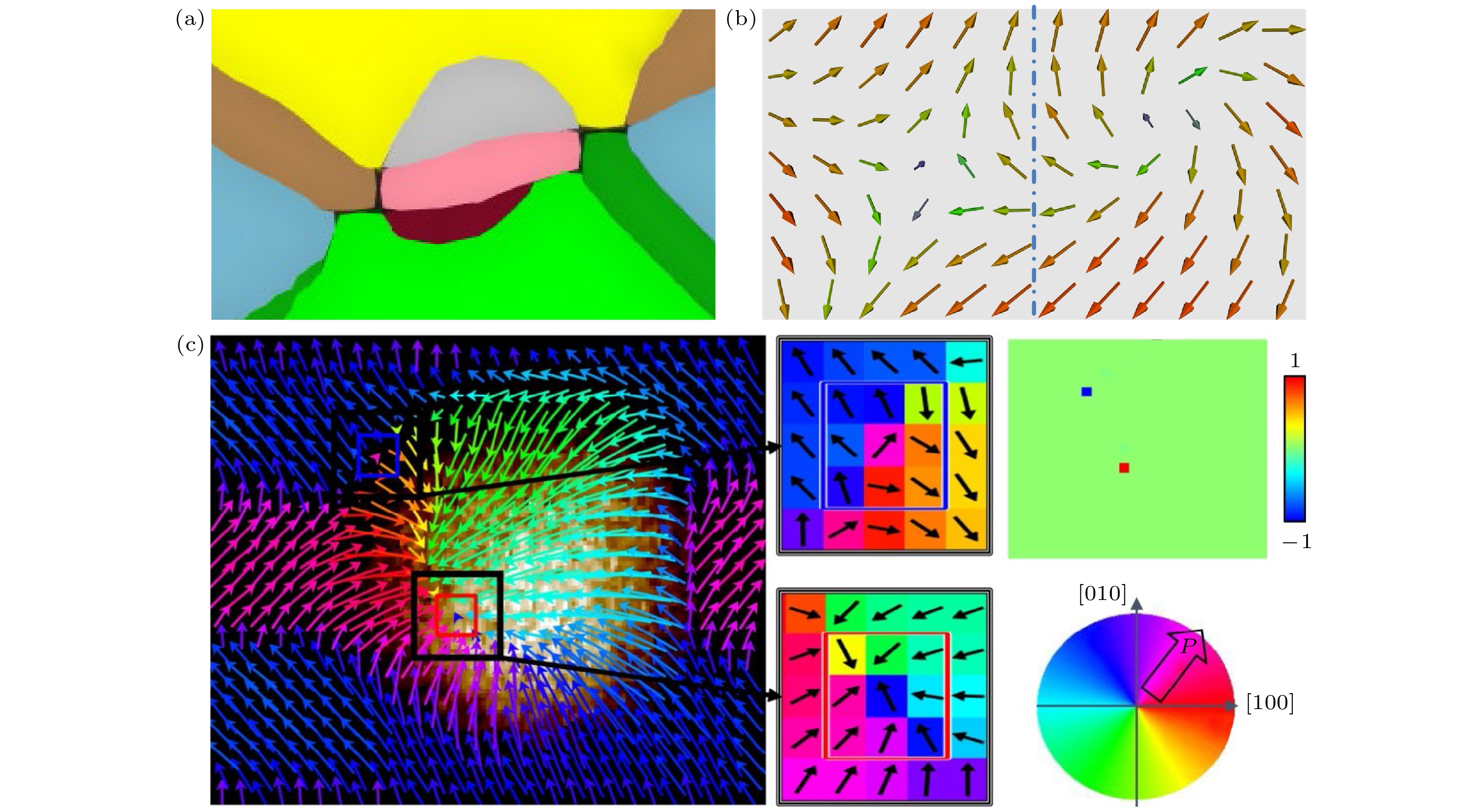
$ {\rm{K}}_{0.5}{\rm{N}\rm{a}}_{0.5}\rm{N}\rm{b}{\rm{O}}_{3} $ )薄膜的电畴结构并进行观察, 根据电场下电畴结构的不同翻转路径将电畴翻转分为快速和慢速翻转阶段, 基于此提出先确定所需实验的电畴翻转状态再进行定向观测的手段. 通过对电畴结构结合极化矢量的分析, 首次在铌酸钾钠薄膜中观察到明显多畴组合而成的涡旋-反涡旋对拓扑结构. 对涡旋结构进一步分析其翻转过程, 观察到这种涡旋拓扑微观结构可以使电畴更容易发生翻转, 从而使更多小范围极化矢量进行排序, 以形成所需的多粒子系统拓扑结构. 这种极化矢量排序对铁电材料介电性能改善机制, 是与准同型相界两侧特定极化方向所形成的微观相界有着异曲同工之处.The perovskite crystal structure determines the appearance of ferroelectricity and the polarization direction of ferroelectric ceramics. When the polarization direction has a certain order, different domain structures will combine to form a multiparticle system with a specific morphology, i.e. the topological structure existing in ferroelectrics. In this study, the domain structures of potassium sodium niobate ($ {\rm{K}}_{0.5}{\rm{N}\rm{a}}_{0.5}\rm{N}\rm{b}{\rm{O}}_{3} $ ) thin films under different hysteresis electric fields and thickness are simulated and observed by the phase field method. According to the different switching paths of the domain structure under the electric field, the domain is divided into fast and slow switching process. Based on this, a method is proposed to first determine the domain switching state of the desired experiment and then conduct directional observation. Through the analysis of the domain structures combined with the polarization vector, a clear multi-domain combined with vortex-antivortex pair topological structure is observed for the first time in$ {\rm{K}}_{0.5}{\rm{N}\rm{a}}_{0.5}\rm{N}\rm{b}{\rm{O}}_{3} $ film. The vortex structure is further analyzed for its switching process, and it is observed that this vortex topological microstructure can make the domain more likely to switch, so that more small-scale polarization vectors can be ordered, forming the desired multiparticle system topology. The mechanism of improving the dielectric properties of ferroelectric material by this polarization vector ordering is similar to that of the microscopic phase boundary formed by the specific polarization directions on both sides of the quasi morphotropic phase boundary.-
Keywords:
- ferroelectric ceramics /
- topological defects /
- phase field method
[1] Wada S, Muraoka K, Kakemoto H, Tsurumi T, Kumagai H 2004 Jpn. J. Appl. Phys. 43 6692
 Google Scholar
[2] Wang B, Li F, Chen L Q 2021 Adv. Mater. 33 2105071
Google Scholar
[3] Braun H B 2012 Adv. Phys. 61 1
Google Scholar
[4] Toulouse G, Kléman M 1976 Journal de Physique Lettres 37 149
Google Scholar
[5] Kittel C 1949 Rev. Mod. Phys. 21 541
Google Scholar
[6] Chen S, Yuan S, Hou Z P, Tang Y L, Zhang J P, Wang T, Li K, Zhao W W, Liu X J, Chen L, Martin L W, Chen Z H 2021 Adv. Mater. 33 2000857
Google Scholar
[7] Fu H, Bellaiche L 2003 Phys. Rev. Lett. 91 257601
Google Scholar
[8] Kornev I, Fu H, Bellaiche L 2004 Phys. Rev. Lett. 93 196104
Google Scholar
[9] Naumov I I, Bellaiche L, Fu H 2004 Nature 432 737
Google Scholar
[10] Prosandeev S, Bellaiche L 2007 Phys. Rev. B 75 172109
Google Scholar
[11] Hong J W, Catalan G, Fang D N, Artacho E, Scott J F 2010 Phys. Rev. B 81 172101
Google Scholar
[12] Shimada T, Wang X, Kondo Y, Kitamura T 2012 Phys. Rev. Lett. 108 067601
Google Scholar
[13] Vasudevan R K, Chen Y C, Tai H H, Balke N, Wu P, Bhattacharya S, Chen L Q, Chu Y H, Lin I N, Kalinin S V, Nagarajan V 2011 ACS Nano 5 879
Google Scholar
[14] Jia C L, Urban K W, Alexe M, Hesse D, Vrejoiu I 2011 Science 331 1420
Google Scholar
[15] Matsumoto T, Ishikawa R, Tohei T, Kimura H, Yao Q, Zhao H, Wang X, Chen D, Cheng Z, Shibata N, Ikuhara Y 2013 Nano Lett. 13 4594
Google Scholar
[16] Tang Y L, Zhu Y L, Ma X L, Borisevich A Y, Morozovska A N, Eliseev E A, Wang W Y, Wang Y J, Xu Y B, Zhang Z D, Pennycook S J 2015 Science 348 547
Google Scholar
[17] Chu K, Yang C H 2018 Rev. Sci. Instrum. 89 123704
Google Scholar
[18] Kim J, You M, Kim K E, Chu K, Yang C H 2019 npj Quantum Mater. 4 29
Google Scholar
[19] Li Z, Shen H, Dawson G, Zhang Z, Wang Y, Nan F, Song G, Li G, Wu Y, Liu H 2022 J. Mater. Chem. C 10 3071
Google Scholar
[20] Bai G, Ma W 2010 Physica B 405 1901
Google Scholar
[21] Ke X Q, Wang D, Ren X, Wang Y 2013 Phys. Rev. B 88 214105
Google Scholar
[22] Schwarzkopf J, Braun D, Hanke M, Kwasniewski A, Sellmann J, Schmidbauer M 2016 J. Appl. Crystallogr. 49 375
Google Scholar
[23] Schwarzkopf J, Braun D, Hanke M, Uecker R, Schmidbauer M 2017 Front. Mater. 4 26
Google Scholar
[24] Wang Y K, Bin Anooz S, Niu G, Schmidbauer M, Wang L Y, Ren W, Schwarzkopf J 2022 Phys. Rev. Mater. 6 084413
Google Scholar
[25] von Helden L, Schmidbauer M, Liang S J, Hanke M, Wordenweber R, Schwarzkopf J 2018 Nanotechnology 29 415704
Google Scholar
[26] Zhou M J, Wang B, Ladera A, Bogula L, Liu H X, Chen L Q, Nan C W 2021 Acta Mater. 215 117038
Google Scholar
[27] Chen L Q, Shen J 1998 Comput. Phys. Commun. 108 147
Google Scholar
[28] Pohlmann H, Wang J J, Wang B, Chen L Q 2017 Appl. Phys. Lett. 110 102906
Google Scholar
[29] Scott J F, Paz de Araujo C A 1989 Science 246 1400
Google Scholar
[30] Li Y L, Hu S Y, Liu Z K, Chen L Q 2002 Acta Mater. 50 395
Google Scholar
[31] Luo J, Zhang S, Zhou Z, Zhang Y, Lee H Y, Yue Z, Li J F 2019 J. Am. Ceram. Soc. 102 2770
Google Scholar
[32] Wang B, Chen H N, Wang J J, Chen L Q 2019 Appl. Phys. Lett. 115 092902
Google Scholar
[33] https://www.mupro.co/ [2022-9-28]
[34] Nagaosa N, Tokura Y 2013 Nat. Nanotechnol. 8 899
Google Scholar
[35] Xue F, Wang X, Shi Y, Cheong S W, Chen L Q 2017 Phys. Rev. B 96 104109
Google Scholar
[36] Trieloff M, Jessberger E K, Herrwerth I, Hopp J, Fieni C, Ghelis M, Bourot-Denise M, Pellas P 2003 Nature 422 502
Google Scholar
[37] Yang W, Tian G, Fan H, Zhao Y, Chen H, Zhang L, Wang Y, Fan Z, Hou Z, Chen D, Gao J, Zeng M, Lu X, Qin M, Gao X, Liu J M 2022 Adv. Mater. 34 e2107711
Google Scholar
[38] Yan M, Wang H, Campbell C E 2008 J. Magn. Magn. Mater. 320 1937
Google Scholar
[39] Vasudevan R K, Liu Y, Li J, Liang W I, Kumar A, Jesse S, Chen Y C, Chu Y H, Nagarajan V, Kalinin S V 2011 Nano Lett. 11 3346
Google Scholar
[40] Ke X, Wang D, Ren X, Wang Y 2020 Phys. Rev. Lett. 125 127602
Google Scholar
[41] Sato Y, Hirayama T, Ikuhara Y 2011 Phys. Rev. Lett. 107 187601
Google Scholar
[42] Janolin P E 2009 J. Mater. Sci. 44 5025
Google Scholar
-
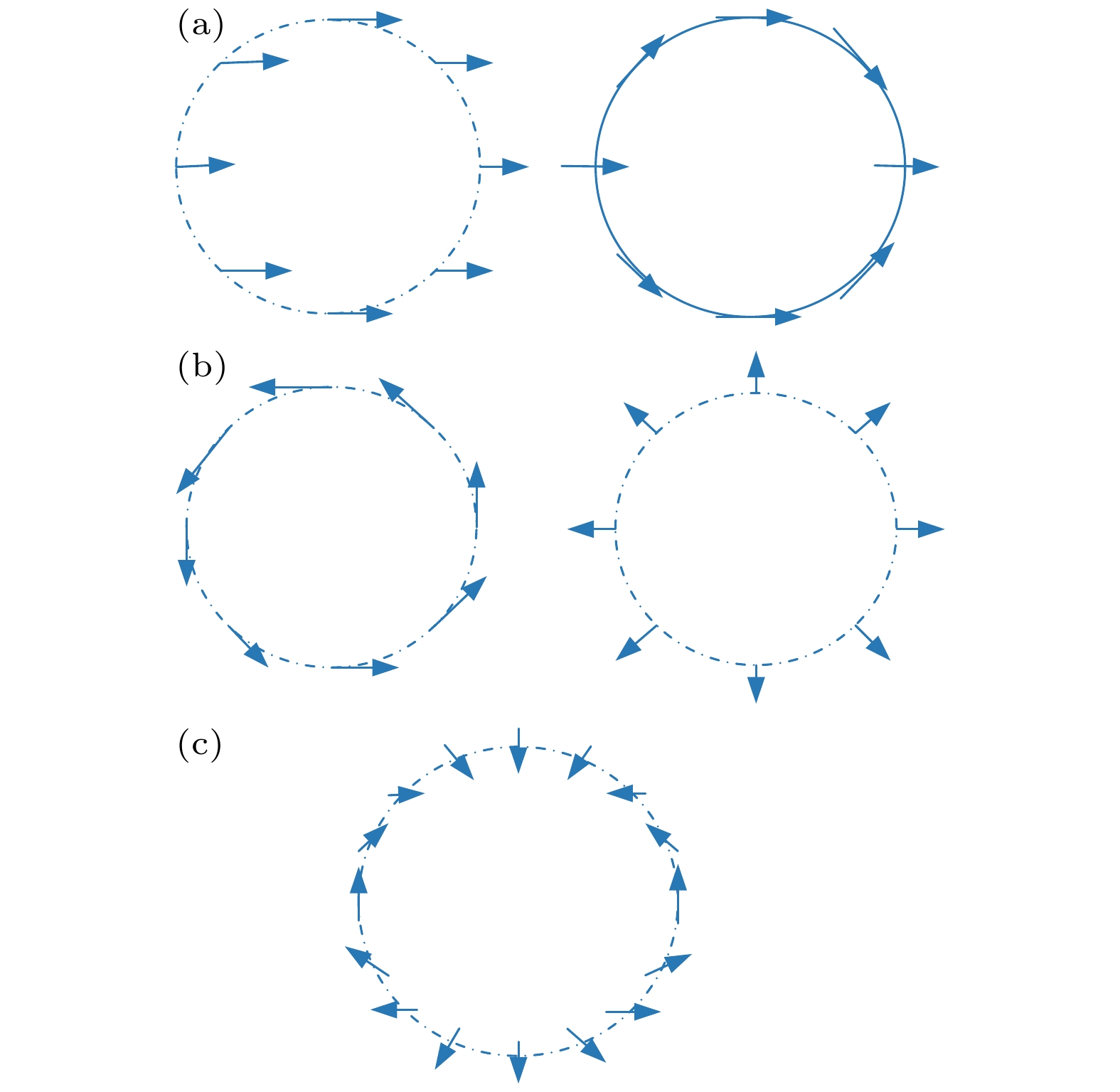
图 2 平面内涡旋结构示意图 (a) w = 0; (b) w = 1; (c) w = 2
Fig. 2. Schematic diagrams of in-plane vortex structure: (a) w = 0; (b) w = 1; (c) w = 2.

图 4 (a)—(f)快速翻转电畴结构图, 其中(a) t = 1110, (b) t = 1120, (c) t = 1140, (d) t = 1150, (e) t = 1160, (f) t = 1170; (g)—(i) 慢速翻转电畴结构图, 其中(g) t = 1300, (h) t = 1400, (i) t = 1500
Fig. 4. (a)–(f) Diagrams of domain structure at fast speed: (a) t = 1110; (b) t = 1120; (c) t = 1140; (d) t = 1150; (e) t = 1160; (f) t = 1170. (g)–(i) Diagrams of domain structure at slow speed: (g) t = 1300; (h) t = 1400; (i) t = 1500.

图 5 电畴含量变化图 (a) 总电畴变化; (b) R畴变化; (c) O畴变化
Fig. 5. Domain composition change diagrams: (a) Total domain change; (b) R domain change; (c) O domain change.

图 6 两种电畴翻转阶段的能量密度 (a) 快速电畴翻转阶段; (b) 慢速电畴翻转阶段
Fig. 6. Energy density of two domain switching stages: (a) Fast domain switch section; (b) slow domain switch section.
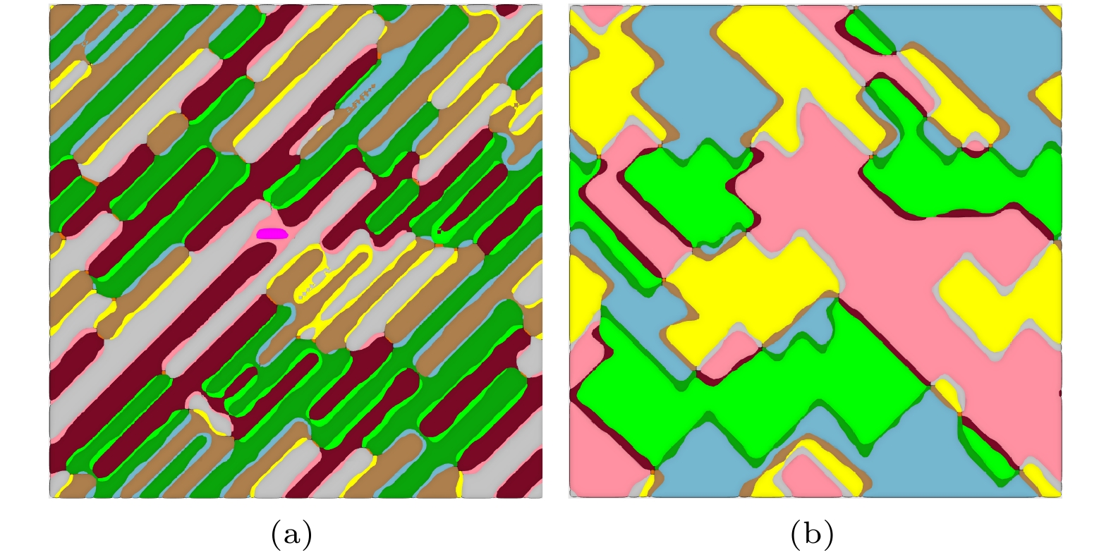
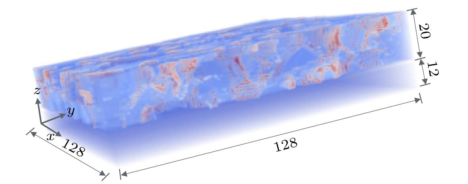
图 7 1100步滞后电场处理后电畴结构 (a) 顶层条纹畴结构; (b) 底层涡旋畴结构
Fig. 7. Domain structures after 1100-step hysteresis electric field loading: (a) Top-layer striped domain structure; (b) bottom-layer vortex domain structure.

图 8 (a)—(c) 不同厚度下的底层(上图)和顶层(下图)电畴结构图, 其中(a) 20 nm, (b) 10 nm, (c) 6 nm; (d)—(i) 涡旋电畴结构翻转过程, 其中(d) t = 20, (e) t = 40, (f) t = 50, (g) t = 60, (h) t = 70, (i) t = 80
Fig. 8. (a)–(c) Bottom (upper panel) and top (bottom panel) layer domain structures at different thicknesses: (a) 20 nm; (b) 10 nm; (c) 6 nm. (d)–(i) Vortex domain structure switching stages: (d) t = 20; (e) t = 40; (f) t = 50; (g) t = 60; (h) t = 70; (i) t = 80.

图 9 (a)—(c) 三种不同厚度体系能量, 其中(a) 弹性能密度, (b) 电场能密度, (c) 朗道能密度; (d) 三种不同厚度的电滞回线
Fig. 9. (a)–(c) Energy of system with three different thicknesses: (a) Elastic energy density; (b) electrostatic energy density; (c) landau energy density. (d) P-E loops with three different thicknesses.
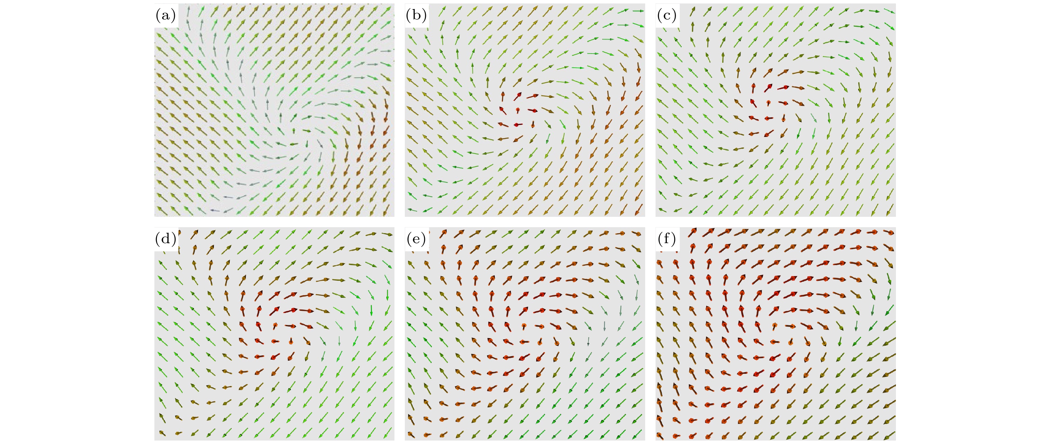
图 10 电畴翻转过程中涡旋的变化 (a) t = 20; (b) t = 40; (c) t = 50; (d) t = 60; (e) t = 70; (f) t = 80
Fig. 10. Vortex change in domain switching process: (a) t = 20; (b) t = 40; (c) t = 50; (d) t = 60; (e) t = 70; (f) t = 80.
-
[1] Wada S, Muraoka K, Kakemoto H, Tsurumi T, Kumagai H 2004 Jpn. J. Appl. Phys. 43 6692
Google Scholar
[2] Wang B, Li F, Chen L Q 2021 Adv. Mater. 33 2105071
Google Scholar
[3] Braun H B 2012 Adv. Phys. 61 1
Google Scholar
[4] Toulouse G, Kléman M 1976 Journal de Physique Lettres 37 149
Google Scholar
[5] Kittel C 1949 Rev. Mod. Phys. 21 541
Google Scholar
[6] Chen S, Yuan S, Hou Z P, Tang Y L, Zhang J P, Wang T, Li K, Zhao W W, Liu X J, Chen L, Martin L W, Chen Z H 2021 Adv. Mater. 33 2000857
Google Scholar
[7] Fu H, Bellaiche L 2003 Phys. Rev. Lett. 91 257601
Google Scholar
[8] Kornev I, Fu H, Bellaiche L 2004 Phys. Rev. Lett. 93 196104
Google Scholar
[9] Naumov I I, Bellaiche L, Fu H 2004 Nature 432 737
Google Scholar
[10] Prosandeev S, Bellaiche L 2007 Phys. Rev. B 75 172109
Google Scholar
[11] Hong J W, Catalan G, Fang D N, Artacho E, Scott J F 2010 Phys. Rev. B 81 172101
Google Scholar
[12] Shimada T, Wang X, Kondo Y, Kitamura T 2012 Phys. Rev. Lett. 108 067601
Google Scholar
[13] Vasudevan R K, Chen Y C, Tai H H, Balke N, Wu P, Bhattacharya S, Chen L Q, Chu Y H, Lin I N, Kalinin S V, Nagarajan V 2011 ACS Nano 5 879
Google Scholar
[14] Jia C L, Urban K W, Alexe M, Hesse D, Vrejoiu I 2011 Science 331 1420
Google Scholar
[15] Matsumoto T, Ishikawa R, Tohei T, Kimura H, Yao Q, Zhao H, Wang X, Chen D, Cheng Z, Shibata N, Ikuhara Y 2013 Nano Lett. 13 4594
Google Scholar
[16] Tang Y L, Zhu Y L, Ma X L, Borisevich A Y, Morozovska A N, Eliseev E A, Wang W Y, Wang Y J, Xu Y B, Zhang Z D, Pennycook S J 2015 Science 348 547
Google Scholar
[17] Chu K, Yang C H 2018 Rev. Sci. Instrum. 89 123704
Google Scholar
[18] Kim J, You M, Kim K E, Chu K, Yang C H 2019 npj Quantum Mater. 4 29
Google Scholar
[19] Li Z, Shen H, Dawson G, Zhang Z, Wang Y, Nan F, Song G, Li G, Wu Y, Liu H 2022 J. Mater. Chem. C 10 3071
Google Scholar
[20] Bai G, Ma W 2010 Physica B 405 1901
Google Scholar
[21] Ke X Q, Wang D, Ren X, Wang Y 2013 Phys. Rev. B 88 214105
Google Scholar
[22] Schwarzkopf J, Braun D, Hanke M, Kwasniewski A, Sellmann J, Schmidbauer M 2016 J. Appl. Crystallogr. 49 375
Google Scholar
[23] Schwarzkopf J, Braun D, Hanke M, Uecker R, Schmidbauer M 2017 Front. Mater. 4 26
Google Scholar
[24] Wang Y K, Bin Anooz S, Niu G, Schmidbauer M, Wang L Y, Ren W, Schwarzkopf J 2022 Phys. Rev. Mater. 6 084413
Google Scholar
[25] von Helden L, Schmidbauer M, Liang S J, Hanke M, Wordenweber R, Schwarzkopf J 2018 Nanotechnology 29 415704
Google Scholar
[26] Zhou M J, Wang B, Ladera A, Bogula L, Liu H X, Chen L Q, Nan C W 2021 Acta Mater. 215 117038
Google Scholar
[27] Chen L Q, Shen J 1998 Comput. Phys. Commun. 108 147
Google Scholar
[28] Pohlmann H, Wang J J, Wang B, Chen L Q 2017 Appl. Phys. Lett. 110 102906
Google Scholar
[29] Scott J F, Paz de Araujo C A 1989 Science 246 1400
Google Scholar
[30] Li Y L, Hu S Y, Liu Z K, Chen L Q 2002 Acta Mater. 50 395
Google Scholar
[31] Luo J, Zhang S, Zhou Z, Zhang Y, Lee H Y, Yue Z, Li J F 2019 J. Am. Ceram. Soc. 102 2770
Google Scholar
[32] Wang B, Chen H N, Wang J J, Chen L Q 2019 Appl. Phys. Lett. 115 092902
Google Scholar
[33] https://www.mupro.co/ [2022-9-28]
[34] Nagaosa N, Tokura Y 2013 Nat. Nanotechnol. 8 899
Google Scholar
[35] Xue F, Wang X, Shi Y, Cheong S W, Chen L Q 2017 Phys. Rev. B 96 104109
Google Scholar
[36] Trieloff M, Jessberger E K, Herrwerth I, Hopp J, Fieni C, Ghelis M, Bourot-Denise M, Pellas P 2003 Nature 422 502
Google Scholar
[37] Yang W, Tian G, Fan H, Zhao Y, Chen H, Zhang L, Wang Y, Fan Z, Hou Z, Chen D, Gao J, Zeng M, Lu X, Qin M, Gao X, Liu J M 2022 Adv. Mater. 34 e2107711
Google Scholar
[38] Yan M, Wang H, Campbell C E 2008 J. Magn. Magn. Mater. 320 1937
Google Scholar
[39] Vasudevan R K, Liu Y, Li J, Liang W I, Kumar A, Jesse S, Chen Y C, Chu Y H, Nagarajan V, Kalinin S V 2011 Nano Lett. 11 3346
Google Scholar
[40] Ke X, Wang D, Ren X, Wang Y 2020 Phys. Rev. Lett. 125 127602
Google Scholar
[41] Sato Y, Hirayama T, Ikuhara Y 2011 Phys. Rev. Lett. 107 187601
Google Scholar
[42] Janolin P E 2009 J. Mater. Sci. 44 5025
Google Scholar


 下载:
下载:

计量
- 文章访问数: 6951
- PDF下载量: 148
- 被引次数: 0
