


-
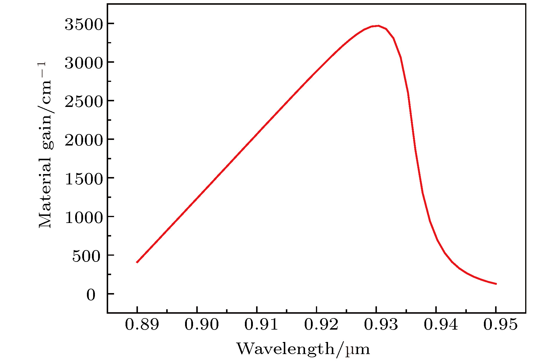
利用PICS3D计算得到InGaAs/GaAsP应变补偿量子阱的增益特性, 得到量子阱的各项参数, 再通过传输矩阵理论和TFCalc膜系设计软件分别仿真出上下分布式布拉格反射镜的白光反射谱. 采用金属有机化合物气相沉积技术外延生长了垂直腔面发射激光器结构, 之后通过干法刻蚀、湿法氧化以及金属电极等芯片技术制备得到8
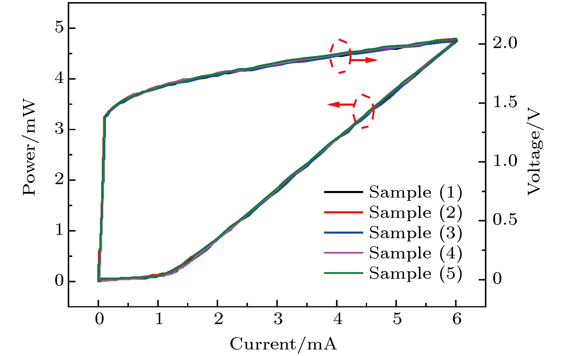
${\text{μm}}$ 氧化孔径的VCSEL芯片. 最终, 测试得到其光电特性实现室温下阈值电流和斜效率分别为0.95 mA和0.96 W/A, 在6 mA电流和2 V电压下输出功率达到4.75 mW, 并测试了VCSEL的高温特性.-
关键词:
- 垂直腔面发射激光器 /
- 分布式布拉格反射镜 /
- 量子阱 /
- 金属有机化合物气相沉积
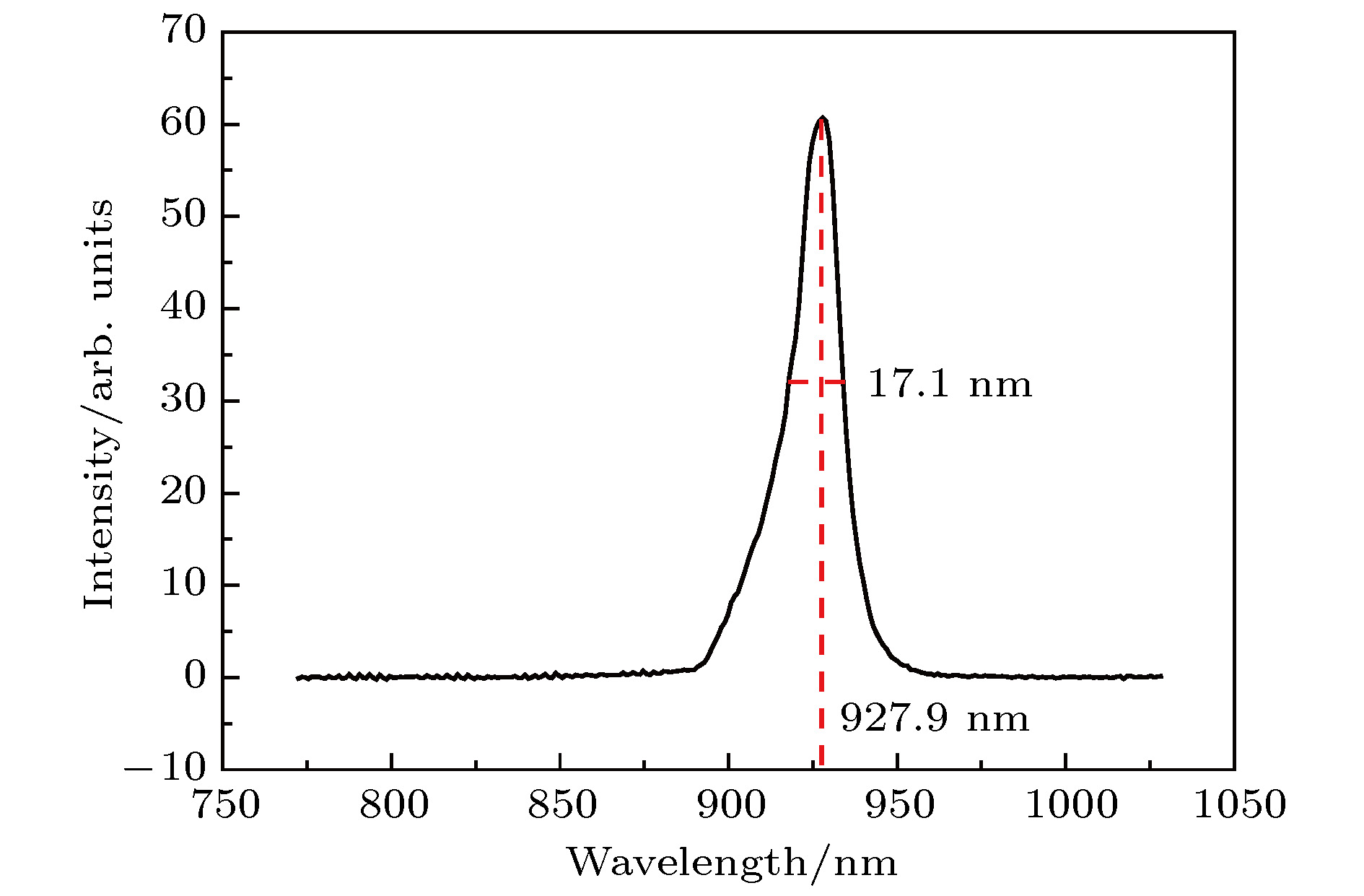
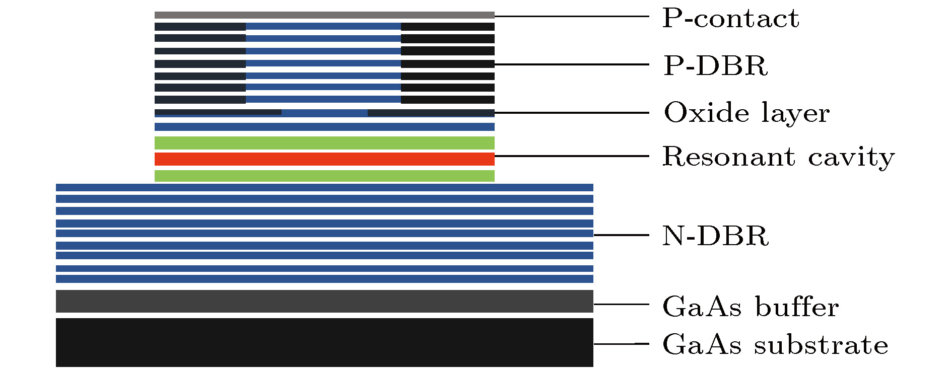
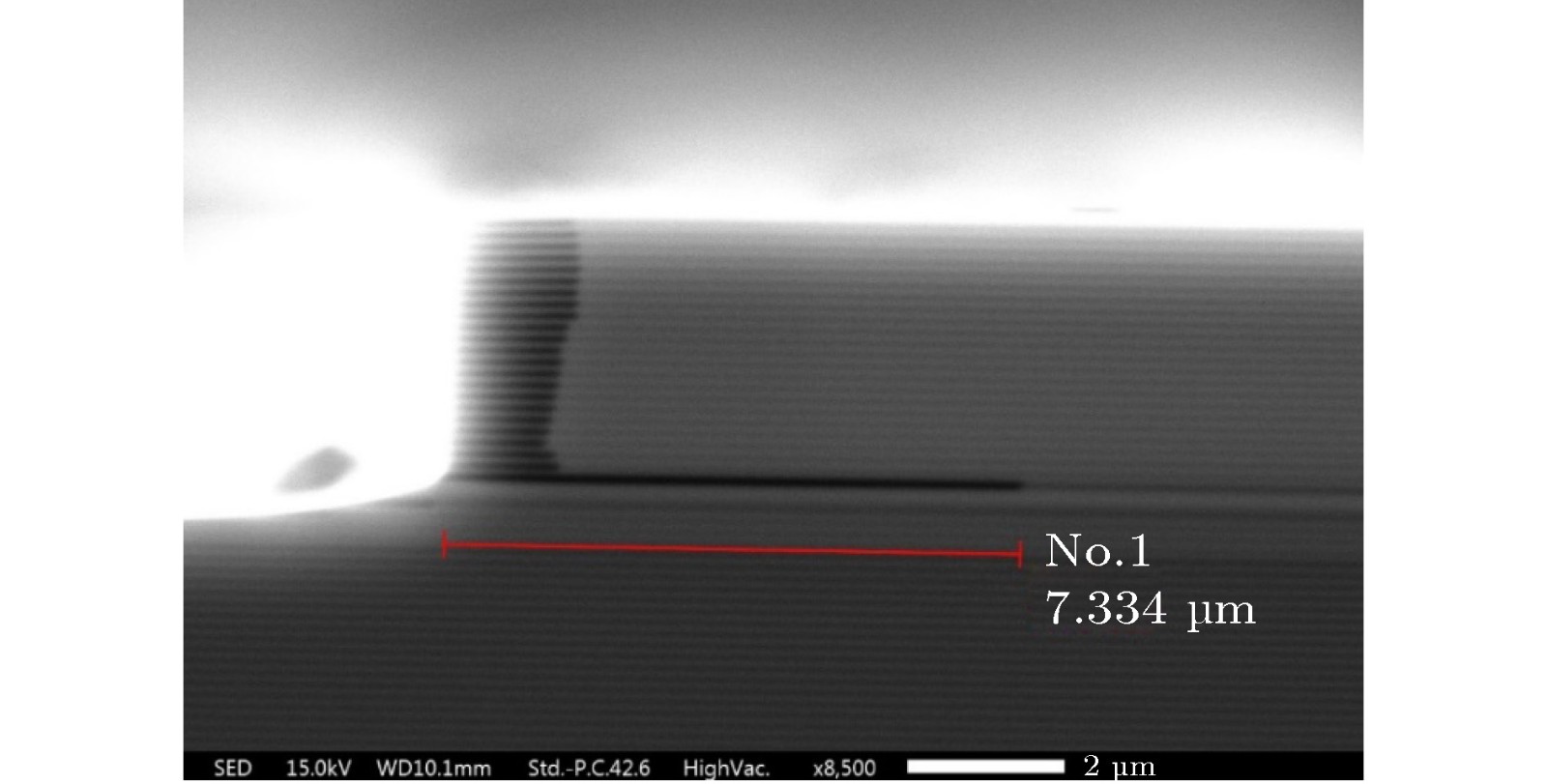
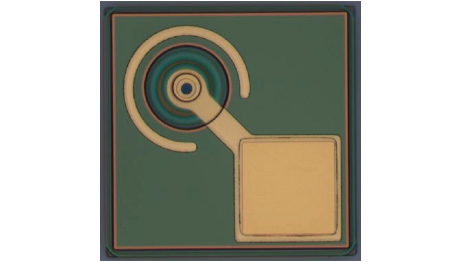
A high slope efficiency vertical-cavity surface-emitting laser (VCSEL) is described. The InGaAs/GaAsP strain compensated multiple quantum wells (MQWs) are designed by PICS3D. The wavelength redshift occurs due to the thermal effect, the lasing wavelength of MQWs is designed to be around 928 nm. The active region consists of five compressively strained 4.4 nm thick In0.16Ga0.84As quantum wells separated and surrounded by 6.2 nm thick GaAs0.88P0.12 tensile strained compensation layers to obtain the high quantum efficiency and ensure the stress release. Subsequently, the MQWs are grown by metal-organic chemical vapor deposition (MOCVD) and the photoluminescence (PL) spectrum is measured using an Nd:YAG laser (532 nm excitation), of which the peak wavelength is approximately 928 nm and the full width at half maximum is nearly 17.1 nm. The resonant cavity is surrounded by p- and n-DBRs. The n-DBRs are designed to be a 28-period AlAs/Al0.12Ga0.88As and 3.5-period Al0.90Ga0.10As/Al0.12Ga0.88As, and the p-DBR is designed to be a 23-period Al0.90Ga0.10As/Al0.12Ga0.88As. The thickness of each a material is$\lambda/4n$ ($\lambda$ = 940 nm, n represents refractive index), and 20 nm graded layer is inserted in the interface between two types of materials. The p-/n-DBRs’ experiment PL reflection spectra (using a white illuminant) are carried out, the central wavelength is around 938.7 nm, and the reflectivity values of p-/n-DBRs are nearly 99.0% and 99.7%, respectively. The VCSELs are grown by MOCVD technique, and treated by dry etching, wet oxidation, metal electrode technology and other processes. In the process of dry etching, the top mesa is treated by inductively coupled plasma with BCl3 and Cl2 chemistry. In order to expose the oxide layer the wet oxidized process is carried out, and the etching depth is nearly 3500 nm. An oxidation furnace is heated for 15 min prior to oxidation. Then the oxide aperture is shaped by the wet nitrogen oxidation furnace at 425 °C with an N2 flow of 200 sccm, and the oxide rate is approximately 0.40${\text{μm}}$ /min for A0.98Ga0.02As. The diameter of oxide aperture is made into an 8${\text{μm}}$ diameter. In the process of metal electrode technology, AuGeNi alloy is sputtered on the top surface to form p-type ohmic contact, and Ti/Pt/Au is evaporated on the back surface of substrate to form an n-type ohmic contact. Rapid thermal annealing at 350 °C in a nitrogen atmosphere is carried out subsequently to obtain a good-quality ohmic contact. Finally, we test the VCSELs’ L-I-V characteristics and spectra in different areas. In area 1, room-temperature lasing at around 940 nm is achieved with a threshold current of 0.95 mA, a slope efficiency of 0.96 W/A, and an output power of 4.75 mW. In area 2, threshold current is 1 mA, a slope efficiency is 0.81 W/A at 25 °C and threshold current is 1.9 mA, slope efficiency is 0.57 W/A at 25 °C. The output power values reach up to 3.850 mW and 2.323 mW at 25 °C and 80 °C, respectively.-
Keywords:
- vertical cavity surface emitting lasers /
- distributed Bragg reflector /
- quantum well /
- metalorganic chemical vapor deposition
[1] Fiebig C, Erbert G, Pittroff W, Wenzel H, Maaßdorf A, Einfeldt S, Tränkle G 2007 Proc. SPIE 6456 64560K
 Google Scholar
[2] Berk Y, Karni Y, Klumel G, Dan Y 2011 The International Society for Optical Engineering San Francisco, USA, February 2–5, 2011 p7918
[3] Grunnet-Jepsen A, Swaminathan K, Keselman L M 2017 US Patent 14998253
[4] Moench H, Gronenborn S, Gu X, Gudde R, Herper M, Kolb J, Miller M, Smeets M, Weigl A 2017 SPIE Photonics West OPTO San Francisco, USA, February 2–7, 2017 p7
[5] Wang T K, Su C Y 2017 US Patent 14841569
[6] Barve A V, Yuen A 2017 US Patent 15638813
[7] Zhou D L, Seurin J F, Xu G Y, Miglo A, Li D Z, Wang Q, Sundaresh M, Wilton S, Matheussen J, Ghosh C 2014 SPIE Photonics West OPTO San Francisco, USA, February 2–7, 2014 p14
[8] Graham L A, Johnson R H, Guenter J K 2016 US Patent 14589392
[9] Larsson A G, Haglund E P, Haglund E, Roelkens G, Gustavsson J, Baets R, Kumasi S 2017 Optical Fiber Communications Conference and Exhibition Los Angeles, USA, March 19–23, 2017 pW3E6
[10] Pusch T, Lindemann M, Gerhardt N C, Hofmann M R, Michalzik R 2015 Electron. Lett. 51 1600
Google Scholar
[11] Gadallah A 2011 IEEE Photon. Technol. Lett. 23 1040
Google Scholar
[12] Haglund E, Gustavsson J S, Sorin W V, Bengtsson J, Fattal D, Haglund Å, Tan M, Larsson A 2017 Proc. SPIE 10113 101130B
Google Scholar
[13] Wang Z F, Ning Y Q, Li T, Cui J J, Zhang Y, Liu G G, Zhang X, Qin L, Liu Y, Wang L J 2009 IEEE Photon. Technol. Lett. 21 239
Google Scholar
[14] Li T, Ning Y Q, Sun Y F, Cui J J, Qin L, Yan C L, Zhang Y, Peng B, Liu G G, Liu Y, Wang L J 2007 Chin. Opt. Lett. 5 S156
[15] 李特, 宁永强, 孙艳芳, 崔锦江, 郝二娟, 秦莉, 套格套, 刘云, 王立军, 崔大复 2007 中国激光 34 641
Google Scholar
Li T, Ning Y Q, Sun Y F, Cui J, Hao E J, Qin L, Tao G T, Liu Y J, Wang L J, Cui D F 2007 Chin. J. Las. 34 641
Google Scholar
[16] 吕朝晨, 王青, 尧舜, 周广正, 于洪岩, 李颖, 郎陆广, 兰天, 张文甲, 梁辰余, 张杨, 赵春风, 贾海峰, 王光辉, 王智勇 2018 光学学报 38 514001
Lü Z C, Wang Q, Yao S, Zhou G Z, Yu H Y, Li Y, Lang L G, Lan T, Zhang W J, Liang C Y, Zhang Y, Zhao C F, Jia H F, Wang G H, Wang Z Y 2018 Acta Opt. Sin. 38 514001
[17] 周广正, 尧舜, 于洪岩, 吕朝晨, 王青, 周天宝, 李颖, 兰天, 夏宇, 郎陆广, 程立文, 董国亮, 康联鸿, 王智勇 2018 物理学报 67 104205
Google Scholar
Zhou G Z, Yao S, Yu H Y, Lü Z C, Wang Q, Zhou T B, Li Y, Lan T, Xia Y, Lang L G, Cheng L W, Dong G L, Kang L H, Wang Z Y 2018 Acta Phys. Sin. 67 104205
Google Scholar
[18] Yu H Y, Yao S, Zhou G Z, Wang Q, Lan T, Lü Z C, Li Y, Lang L G, Zhou T B, Cheng L W 2018 Opt. Quantum Electron. 50 171
Google Scholar
[19] Guo X, Dong J, He X Y, Hu S, He Y, Lü B S, Li C 2017 J. Appl. Phys. 121 133105
Google Scholar
[20] Adachi S 1998 J. Appl. Phys. 58 R1
[21] Pearsall T P 1982 GaInAsP Alloy Semiconductors (New York: Wiley) p3
[22] Chuang S L 2009 Physics of Photonic Devices (New York: Wiley) pp45–52
[23] Surhone L M, Timpledon M T, Marseken S F 2010 Thin-film Optics (Hong Kong: Betascript) pp146–155
-
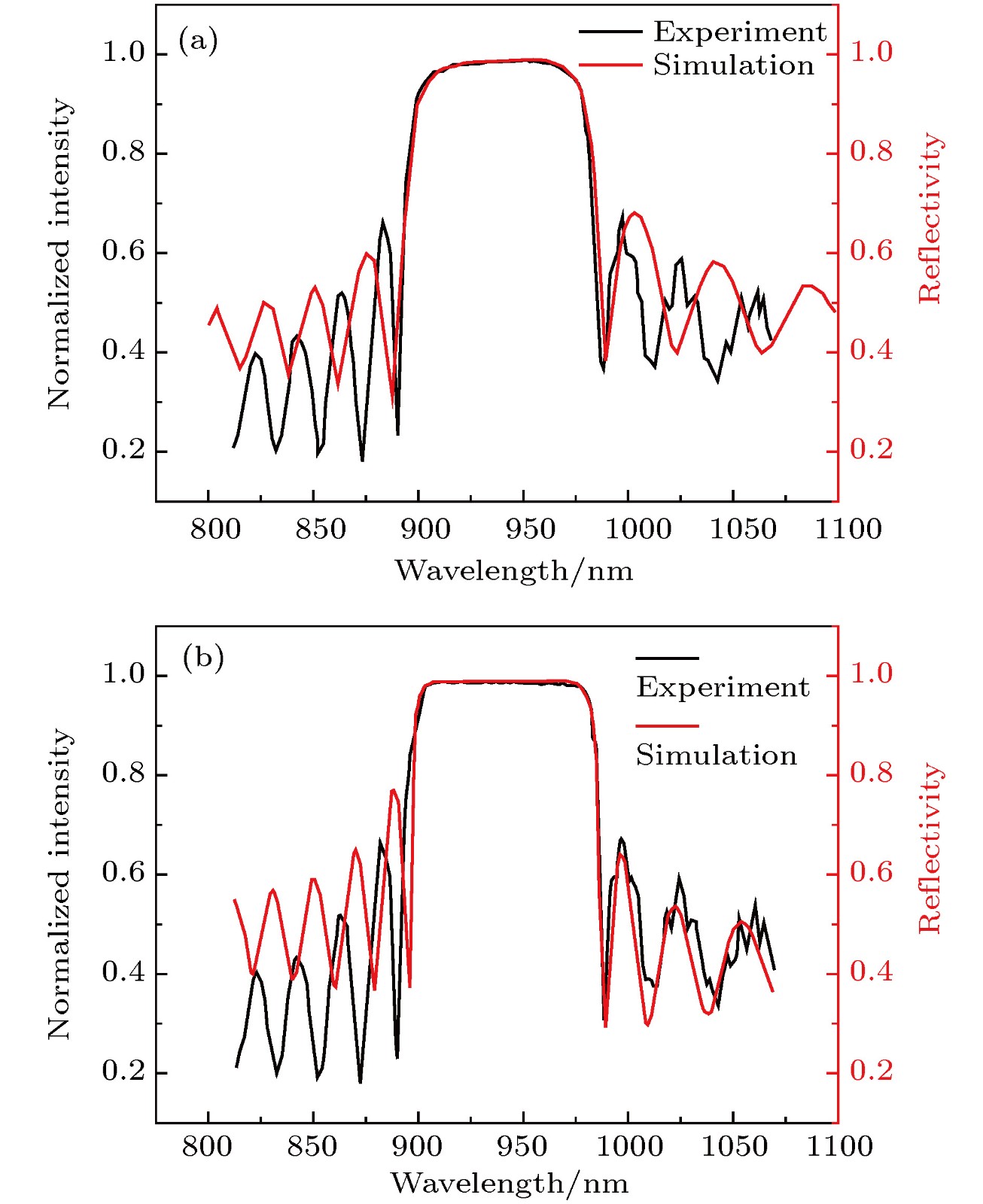
图 4 (a)p-DBRs PL反射谱; (b) n-DBRs PL反射谱
Fig. 4. (a) The PL reflection spectra of p-DBRs; (b) the PL reflection spectra of n-DBRs.
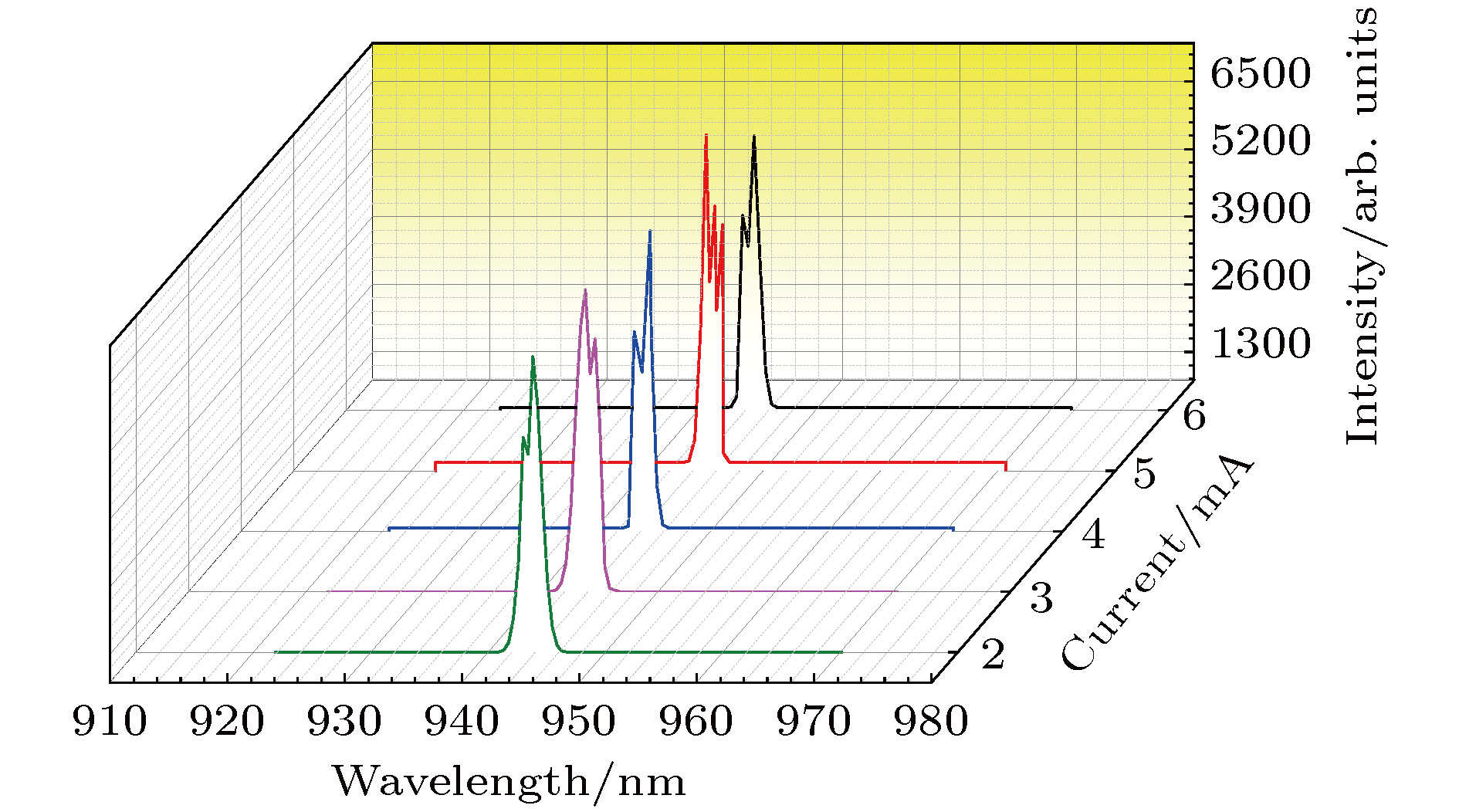
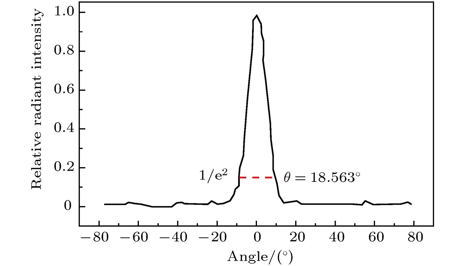
图 11 室温下不同电流的光谱图
Fig. 11. Emission spectra for VCSELs at various injection current at room temperature.
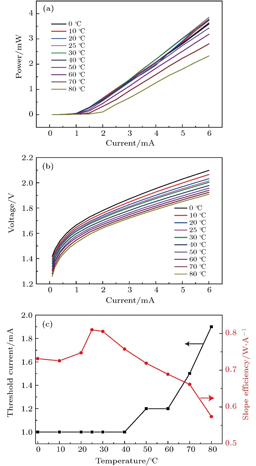
图 12 VCSEL的L-I-V特性曲线 (a)光功率特性; (b)电压电流特性; (c)阈值电流和斜效率随温度变化
Fig. 12. The L-I-V characteristics of VCSELs at various temperature: (a) Output power versus injection current; (b) voltage versus injection current; (c) the evolution of the threshold current and slope efficiency as a function of temperature.
-
[1] Fiebig C, Erbert G, Pittroff W, Wenzel H, Maaßdorf A, Einfeldt S, Tränkle G 2007 Proc. SPIE 6456 64560K
Google Scholar
[2] Berk Y, Karni Y, Klumel G, Dan Y 2011 The International Society for Optical Engineering San Francisco, USA, February 2–5, 2011 p7918
[3] Grunnet-Jepsen A, Swaminathan K, Keselman L M 2017 US Patent 14998253
[4] Moench H, Gronenborn S, Gu X, Gudde R, Herper M, Kolb J, Miller M, Smeets M, Weigl A 2017 SPIE Photonics West OPTO San Francisco, USA, February 2–7, 2017 p7
[5] Wang T K, Su C Y 2017 US Patent 14841569
[6] Barve A V, Yuen A 2017 US Patent 15638813
[7] Zhou D L, Seurin J F, Xu G Y, Miglo A, Li D Z, Wang Q, Sundaresh M, Wilton S, Matheussen J, Ghosh C 2014 SPIE Photonics West OPTO San Francisco, USA, February 2–7, 2014 p14
[8] Graham L A, Johnson R H, Guenter J K 2016 US Patent 14589392
[9] Larsson A G, Haglund E P, Haglund E, Roelkens G, Gustavsson J, Baets R, Kumasi S 2017 Optical Fiber Communications Conference and Exhibition Los Angeles, USA, March 19–23, 2017 pW3E6
[10] Pusch T, Lindemann M, Gerhardt N C, Hofmann M R, Michalzik R 2015 Electron. Lett. 51 1600
Google Scholar
[11] Gadallah A 2011 IEEE Photon. Technol. Lett. 23 1040
Google Scholar
[12] Haglund E, Gustavsson J S, Sorin W V, Bengtsson J, Fattal D, Haglund Å, Tan M, Larsson A 2017 Proc. SPIE 10113 101130B
Google Scholar
[13] Wang Z F, Ning Y Q, Li T, Cui J J, Zhang Y, Liu G G, Zhang X, Qin L, Liu Y, Wang L J 2009 IEEE Photon. Technol. Lett. 21 239
Google Scholar
[14] Li T, Ning Y Q, Sun Y F, Cui J J, Qin L, Yan C L, Zhang Y, Peng B, Liu G G, Liu Y, Wang L J 2007 Chin. Opt. Lett. 5 S156
[15] 李特, 宁永强, 孙艳芳, 崔锦江, 郝二娟, 秦莉, 套格套, 刘云, 王立军, 崔大复 2007 中国激光 34 641
Google Scholar
Li T, Ning Y Q, Sun Y F, Cui J, Hao E J, Qin L, Tao G T, Liu Y J, Wang L J, Cui D F 2007 Chin. J. Las. 34 641
Google Scholar
[16] 吕朝晨, 王青, 尧舜, 周广正, 于洪岩, 李颖, 郎陆广, 兰天, 张文甲, 梁辰余, 张杨, 赵春风, 贾海峰, 王光辉, 王智勇 2018 光学学报 38 514001
Lü Z C, Wang Q, Yao S, Zhou G Z, Yu H Y, Li Y, Lang L G, Lan T, Zhang W J, Liang C Y, Zhang Y, Zhao C F, Jia H F, Wang G H, Wang Z Y 2018 Acta Opt. Sin. 38 514001
[17] 周广正, 尧舜, 于洪岩, 吕朝晨, 王青, 周天宝, 李颖, 兰天, 夏宇, 郎陆广, 程立文, 董国亮, 康联鸿, 王智勇 2018 物理学报 67 104205
Google Scholar
Zhou G Z, Yao S, Yu H Y, Lü Z C, Wang Q, Zhou T B, Li Y, Lan T, Xia Y, Lang L G, Cheng L W, Dong G L, Kang L H, Wang Z Y 2018 Acta Phys. Sin. 67 104205
Google Scholar
[18] Yu H Y, Yao S, Zhou G Z, Wang Q, Lan T, Lü Z C, Li Y, Lang L G, Zhou T B, Cheng L W 2018 Opt. Quantum Electron. 50 171
Google Scholar
[19] Guo X, Dong J, He X Y, Hu S, He Y, Lü B S, Li C 2017 J. Appl. Phys. 121 133105
Google Scholar
[20] Adachi S 1998 J. Appl. Phys. 58 R1
[21] Pearsall T P 1982 GaInAsP Alloy Semiconductors (New York: Wiley) p3
[22] Chuang S L 2009 Physics of Photonic Devices (New York: Wiley) pp45–52
[23] Surhone L M, Timpledon M T, Marseken S F 2010 Thin-film Optics (Hong Kong: Betascript) pp146–155


 下载:
下载:


计量
- 文章访问数: 18991
- PDF下载量: 549
- 被引次数: 0
