搜索

x

留言板

尊敬的读者、作者、审稿人, 关于本刊的投稿、审稿、编辑和出版的任何问题, 您可以本页添加留言。我们将尽快给您答复。谢谢您的支持!

姓名
邮箱
手机号码
标题
留言内容
验证码

Weibel不稳定性自生电磁场对探针质子束的偏转作用研究

杜报 蔡洪波 张文帅 陈京 邹士阳 朱少平

Cang Shi-Jian, Chen Zeng-Qiang, Yuan Zhu-Zhi. Analysis and circuit implementation of a new four-dimensional non-autonomous hyper-chaotic system. Acta Phys. Sin., 2008, 57(3): 1493-1501. doi: 10.7498/aps.57.1493
Citation: Cang Shi-Jian, Chen Zeng-Qiang, Yuan Zhu-Zhi. Analysis and circuit implementation of a new four-dimensional non-autonomous hyper-chaotic system. Acta Phys. Sin., 2008, 57(3): 1493-1501. doi: 10.7498/aps.57.1493

Weibel不稳定性自生电磁场对探针质子束的偏转作用研究

杜报, 蔡洪波, 张文帅, 陈京, 邹士阳, 朱少平

Deflection effect of electromagnetic field generated byWeibel instability on proton probe

Du Bao, Cai Hong-Bo, Zhang Wen-Shuai, Chen Jing, Zou Shi-Yang, Zhu Shao-Ping
Article Text (iFLYTEK Translation)
PDF
HTML
导出引用
  • Weibel不稳定性的自生电磁场对于等离子体能量输运、无碰撞冲击波形成等物理过程具有关键的影响. 实验上往往采用质子束照相来诊断其电磁场结构. 一般认为, 探针质子束的轨迹偏转主要来自于磁场, 而自生电场的作用被认为可忽略不计. 本文利用三维粒子模拟程序研究了典型参数下的Weibel不稳定性发展过程, 并使用径迹追踪法评估了Weibel不稳定性的质子束照相过程中电场和磁场对探针质子束的偏转作用. 对比分析发现, 引起探针质子束偏转的主要因素并不是磁场, 而是过去研究中常被忽略的电场. 主要原因为: Weibel不稳定性的自生磁场往往成管状结构, 在使用探针质子束对其进行侧向照相时, 磁场的作用会被自身中和并抵消. 该认识将有助于深入理解Weibel不稳定性质子照相的实验结果.
    The electric and magnetic fields generated by the Weibel instability, most of which have a tube-like structure, are of importance for many relevant physical processes in the astrophysics and the inertial confinement fusion. Experimentally, proton radiography is a commonly used method to diagnose the Weibel instability, where the proton deflection introduced from the self-generated electric field is usually ignored. This assumption, however, is in conflict with the experimental observations by Quinn, Fox and Huntington, et al. because the magnetic field with a tube-like structure cannot introduce parallel flux striations on the deflection plane in the proton radiography. In this paper, we re-examine the nature of the proton radiography of the Weibel instability numerically. Two symmetric counterstreaming plasma flows are used to generate the electron Weibel instability with the three-dimensional particle-in-cell simulations. The proton radiography of the Weibel instability generated electric and magnetic fields are calculated with the ray tracing method. Three cases are considered andcompared: only the self-generated electric field E is included, only the self-generated magnetic field B is included, both the electric field E and magnetic field B are included. It is shown that when only E is included, the probe proton flux density perturbation on the detection plane, i.e., δn/n0, is much larger than that when only B is included. Also, when both E and B are included, δn/n0 is almost the same as that when only E is included. This suggests that in the proton radiography of the Weibel instability generated electric and magnetic fields, the deflection from the electric field dominates the radiography, whereas the magnetic field has an ignorable influence. Our conclusion is quite different from that obtained on the traditional assumption that the electric field is ignorable in the radiography. This mainly comes from the spatial structure of the Weibel instability generated magnetic field, which is tube-like and points to the azimuthal direction around the current filaments. When the probe protons pass through the field region, the deflection from the azimuthal magnetic field can be compensated for completely by itself along the passing trajectories especially if the deflection distance inside the field region is small. Whereas for the electric field, which is in the radial direction, the deflection to the probe protons will not be totally compensated for and will finally introduce an evident flux density perturbation into the detection plane. This understanding can beconducive to the comprehension of the experimental results about the proton radiography of the Weibel instability.
      通信作者: 蔡洪波, Cai_hongbo@iapcm.ac.cn ; 朱少平, zhu_shaoping@iapcm.ac.cn
    • 基金项目: 科学挑战专题(批准号: TZ2016005)、国家重点研发计划(批准号: 2016YFA0401100)、国家自然科学基金联合基金(批准号: U1730449)和国家自然科学基金(批准号: 11575030)资助的课题.
      Corresponding author: Cai Hong-Bo, Cai_hongbo@iapcm.ac.cn ; Zhu Shao-Ping, zhu_shaoping@iapcm.ac.cn
    • Funds: Project supported by the Science Challenge Project, China (Grant No. TZ2016005), the National Key R&D Program of China (Grant No. 2016YFA0401100), the Joint Funds of the National Natural Science Foundation of China (Grant No. U1730449), and the National Natural Science Foundation of China (Grant No. 11575030)

    近年来, 非晶氧化锌镓铟薄膜晶体管(amorphous InGaZnO thin-film transistor, InGaZnO TFT)的研究及其应用广受关注. 由于具有高迁移率、低关态电流、高透光率、均匀性良好以及低温可制备性等优点[1-5], InGaZnO TFT有望取代硅基TFT, 在平板显示、光学图像传感器、触控和指纹传感等领域拥有良好的应用前景[6-9]. 在传统的应用中, 例如薄膜晶体管液晶显示(TFT-LCD), 或者有源矩阵有机发光二极管显示(active-matrix organic light emitting display, AM-OLED), 主要利用的是InGaZnO TFT导通态的电学性能[10-12], 但在InGaZnO TFT集成的众多新兴领域中, 例如光学图像传感器, InGaZnO TFT的泄漏电流特性至关重要.

    以往的研究表明, TFT中常见的泄漏电流产生机制包括陷阱辅助热发射[13,14]、陷阱辅助场发射[13]、带间隧穿[15,16]和包含Poole-Frenkel (PF)效应的陷阱辅助热电子场致发射[17]等. Lui和Migliorato [18]基于PF效应和陷阱辅助隧穿效应, 提出了载流子产生复合速率模型, 其适合于器件的数值计算. Wu等[19]在此基础上提出了多晶硅TFT泄漏电流紧凑模型, 其中包含了PF效应, 无需繁琐的数值计算, 并且可以通过实验数据提取得到模型参数. Servati和Nathan [20]研究了非晶硅(a-Si:H) TFT的泄漏电流的产生来源, 基于欧姆传导模型、反向亚阈传导模型和前沟道传导模型建立了分段式泄漏电流模型. 但是迄今为止, 几乎未见有关InGaZnO TFT的泄漏电流模型的研究报道, 这不利于InGaZnO TFT集成图像传感器等新兴领域的研究.

    本文基于载流子的产生-复合机制建立了InGaZnO TFT的泄漏电流模型. 通过与TCAD模拟以及测试结果的对比来检验所提出的模型. 基于所提出的泄漏电流模型, 分析了InGaZnO TFT的沟道宽度、沟道长度和栅介质层厚度对泄漏电流的影响.

    图1示意了底栅顶接触型InGaZnO TFT的剖面图. 表1列出了InGaZnO TFT器件结构的几何参数, 其中 InGaZnO TFT的沟道宽长比W/L = 300 μm/50 μm, a-InGaZnO半导体层厚度tIGZO = 40 nm, 栅介质层厚度tSiOx=150nm [21].

    图 1 InGaZnO TFT的结构剖面图\r\nFig. 1. Structural cross-section of InGaZnO TFT.
    图 1  InGaZnO TFT的结构剖面图
    Fig. 1.  Structural cross-section of InGaZnO TFT.
    表 1  InGaZnO TFT器件结构的几何参数
    Table 1.  Geometric parameters of InGaZnO TFT device structure.
    参数数值
    栅介质层厚度/nm150
    a-InGaZnO半导体层厚度/nm40
    沟道宽度/μm300
    沟道长度/μm50
    下载: 导出CSV 
    | 显示表格

    图2(a)给出了在实验[21]与TCAD数值模拟中得到的InGaZnO TFT在关断区和亚阈区的IDS-VGS转移特性的曲线对比, 其中VDS取值从2 V增加到10 V. 由图可知, InGaZnO TFT具有较低的泄漏电流, 且IDS随着VDS增大而增加, IDS的变化范围为10–13—10–12 A. 泄漏电流增加的主要原因是随着TFT上所施加偏压的增加, 陷阱态中的电子获得能量跃迁至导带的几率就越大. 实验值和TCAD模拟值的变化趋势及范围大致相同, 在亚阈区内泄漏电流均呈数量级的增长.

    图 2 IGZO TFT电学特性曲线实验与数值模拟比较 (a) IDS-VGS转移特性曲线; (b) IDS-VDS输出特性曲线\r\nFig. 2. The comparison of IGZO TFT electrical characteristic curve in experiment and numerical simulation: (a) IDS-VGS transfer characteristic curve; (b) IDS-VDS output characteristic curve.
    图 2  IGZO TFT电学特性曲线实验与数值模拟比较 (a) IDS-VGS转移特性曲线; (b) IDS-VDS输出特性曲线
    Fig. 2.  The comparison of IGZO TFT electrical characteristic curve in experiment and numerical simulation: (a) IDS-VGS transfer characteristic curve; (b) IDS-VDS output characteristic curve.

    图2(b)为同一InGaZnO TFT IDS-VDS转移特性曲线的实验值和TCAD模拟值的对比, 结果表明IDSVGS, VDS均呈正相关, 在器件的饱和区(VDSVGSVTH), IDS的值趋于稳定且不随VDS发生变化. 从图中可以看出实验值与TCAD模拟值吻合度较高, 说明TCAD模拟较为可靠. 因此, 后续将以TCAD模拟值作为参考, 验证所建立InGaZnO TFT泄漏电流解析模型的可靠性.

    在InGaZnO TFT的TCAD电学仿真中, 主要通过金属功函数和UST (universal Schottky tunnling model)模型描述肖特基势垒; 有源层材料InGaZnO的特性主要由缺陷态(defects)密度模型决定. InGaZnO的缺陷态模型与泄漏电流密切相关, 具体模型参数见表2.

    表 2  InGaZnO缺陷态密度模型参数
    Table 2.  Density of states model parameters for InGaZnO.
    参数描述数值单位
    nta导带尾类受主能态密度1.04 × 1019cm–3·eV–1
    ntd价带尾类施主能态密度5.0 × 1020cm–3·eV–1
    wta类受主态特征能量0.04eV
    wtd类施主态特征能量0.1eV
    nga高斯分布的受主态密度0cm–3·eV–1
    ngd高斯分布的施主态密度2.0 × 1016cm–3·eV–1
    egd高斯分布施主能态峰值能量2.9eV
    wgd高斯分布施主能态特征能量0.1eV
    下载: 导出CSV 
    | 显示表格

    根据陷阱辅助热电子场致发射机制, 在较强的栅-漏电场作用下, 大量电子将从局域态中隧穿到导带[18]. 载流子的产生率与Poole-Frenkel效应和声子辅助隧穿效应密切相关. InGaZnO层带隙内的局域态可表示为

    RT=RA+RD,
    (1)

    其中RT是陷阱态中的载流子产生复合率, RARD分别是受主态和施主态的载流子产生复合率. 作为n沟道器件, InGaZnO TFT中类施主态呈中性, 对自由载流子数量的影响几乎可以忽略. 但是, InGaZnO的类受主态呈正电性, 可捕获自由电子, 对泄漏电流的大小的影响较大. 在建模过程中, 为了简化计算, 忽略了施主态, 只考虑了受主态的载流子产生. 因此(1)式可简化为:

    RT=RA,
    (2)
    RA=npn2in+n1cp(χF+ΓCoulp)+p+p1cn(1+ΓDiracn)NA(Et),
    (3)

    (3)式中NA(Et)是类受主态在导(价)带附近处深能态和带尾态的密度, 受主态包括尾态和深能态级, 由于InGaZnO TFT中深能态级密度远低于带尾态, 因此, 计算过程中主要考虑带尾态密度; χF是Poole-Frenkel增强效应因子; ni是本征载流子浓度; n1p1分别代表陷阱能级上的电子浓度和空穴浓度, cn,p代表俘获系数, 且

    n1=niexp(EtEikT),
    (4)
    p1=niexp(EiEtkT),
    (5)
    χF=exp(ΔECkT),
    (6)

    式中k为玻尔兹曼常数, T为温度; 其中ΔEC可表征为

    ΔEC=qqFπεIGZO,
    (7)

    其中q代表电荷量, F为垂直方向的电场强度, εIGZO为InGaZnO材料的介电常数. (7)式来源于描述Poole-Frenkel效应下泄漏电流与电场强度关系的公式[22], 在Poole-Frenkel效应作用下, 泄漏电流与电场强度的指数正相关, ΔEC表示在电场强度F作用下势垒的降低量. (3)式中ΓpCoulΓDiracn分别是Dirac阱与Coulombic阱中载流子的隧穿比率, 可表征为:

    ΓDiracn=ΔEnkT10exp(ΔEnkTknu32)du,
    (8)
    ΓCoulp=ΔEpkT1ΔECΔEpexp{ΔEpkTukpu32[1(ΔECuΔEp)53]}du,
    (9)

    (8)和(9)式中u=ECEΔEn, 同时

    ΔEn=ECEt,
    (10)
    ΔEp=EtEV,
    (11)
    kn,p=42me,h(ΔEn,p)33qF.
    (12)

    (12)式中me,h表示隧穿效应中电子(空穴)的有效质量, 表示普朗克常数.

    NA(Et)=NTailAexp[EtECETailA],
    (13)
    U=ECEVRT(Et)dEt=ECEVRA(Et)dEt.
    (14)

    将(1)—(13)式代入(14)式中, 可以求解得到InGaZnO TFT的载流子产生率. 在上述模型中, 包含了InGaZnO TFT可能的泄漏电流产生机制: 场致电子发射、带间隧穿以及Poole-Frenkel效应[23-25]. 由于InGaZnO TFT器件一般工作于常温, 热电子发射产生的泄漏电流极小, 这里忽略了热电子发射效应. 同时, (14)式也是一双积分表达式, 计算过程繁琐且需要消耗大量的内存资源. 因此, 本文采用分区段计算的方法来简化建模过程.

    分析式(14)可知, 第一重积分计算的是场效应积分即ΓCouln,pΓDiracn,p的值, 积分对象是u, 积分过程与Poole-Frenkel增强因子χF无关; 第二重积分的对象是Et, 积分过程同样与Poole-Frenkel增强因子χF无关; 在整个积分过程中Poole-Frenkel增强因子χF始终保持指数形式, 在最终积分结果中也保持原状.

    在低负电场区域(FFC), Poole-Frenkel效应增强下的热发射是泄漏电流产生的主要机制, 在载流子产生复合率U的表达式里Poole-Frenkel增强因子χF的值占主导地位, 因此低负电场区载流子产生复合率U可简化成

    U=a1exp(b1F),FFC.
    (15)

    在高负电场区域(FFC), 陷阱中的载流子首先热激发到一个中间能级Et, 然后再从该中间能级隧穿到导带或者价带; 根据文献[26]可知在高负电场区域热离子场助发射是产生泄漏电流的主要原因. 文献[26]中计算得出, 在高负电场区域lnU与电场强度F呈线性关系, 故在高负电场区载流子产生复合率U可表示为

    U=a2exp(b2F),F>FC.
    (16)

    结合(15)和(16)式得到载流子的复合产生率分段方程为

    U={a1exp(b1F),FFC,a2exp(b2F),F>FC,
    (17)

    其中a1, a2, b1, b2均为拟合参数. 泄漏电流ILeak可由(18)式描述[27]:

    ILeak=qVolU,
    (18)

    其中

    Vol=WLovXd,
    (19)

    式中q是电荷量, Vol是源漏极交叠耗尽区的体积, W是InGaZnO TFT沟道宽度, Lov是栅漏交叠区长度, Xd为耗尽区厚度. 将(19)式代入(18)式中得到关断区泄漏电流模型:

    ILeak-off={qVola1exp(b1F),FFC,qVola2exp(b2F),F>FC,
    (20)

    其中

    F=VDSVGStSiOx,
    (21)

    tSiOx为栅氧化层厚度.

    图2(a)可知在亚阈区后半段lnIDSVGS呈线性关系:

    ILeak-sub=a3exp(b3VGS).
    (22)

    使用平滑函数tanh(x)[28]得到InGaZnO TFT泄漏电流的统一模型为

    ILeak=qWLovXd[a1exp[b1(VDSVGStSiOx)]×{1tanh[β(VGSVC)]2}+a2exp(b2VDSVGStSiOx)×(1+tanh[β(VGSVC)]2)]×(1tanh(βVGS)2)+a3exp(b3VGS)[1+tanh(βVGS)2],
    (23)

    其中a1, a2, a3, b1, b2, b3均为拟合参数.

    根据上述模型可得到InGaZnO TFT泄漏电流的计算值, 此外还可利用TCAD模拟的方式得到InGaZnO TFT泄漏电流的模拟值. 图3是模型计算结果和TCAD模拟结果的对比图. 从模拟结果来看, VDS从2 V增大到10 V的过程中, InGaZnO TFT泄漏电流也随之增大. 这与(20)式和(21)式描述的情况相符, VDS增大导致垂直方向电场F增大, 在强电场的作用力下, Poole-Frenkel效应愈加明显, 在陷阱态的电子只需要获得较小的热能便能脱离陷阱态变成自由载流子, 沟道内自由载流子增多使得泄漏电流增大.

    图 3 模型计算值与TCAD模拟值的对比(VDS = 2, 4, 6, 8, 10 V)\r\nFig. 3. Comparison between model calculation and numerical simulation results (VDS = 2, 4, 6, 8, 10 V).
    图 3  模型计算值与TCAD模拟值的对比(VDS = 2, 4, 6, 8, 10 V)
    Fig. 3.  Comparison between model calculation and numerical simulation results (VDS = 2, 4, 6, 8, 10 V).

    图4给出了不同沟道宽度情况下的InGaZnO TFT的TCAD模拟结果和模型计算结果的对比. TFT的沟道宽度W从200 μm增大至500 μm, 泄漏电流随TFT的沟道宽度线性增大. 这与(19)式描述的情况较为符合. 这是因为TFT的沟道宽度W增大导致耗尽区的面积和体积增大, 从而沟道内的感应载流子增多, 致使泄漏电流增大. 由于(19)式中的Lov是指栅漏交叠区域的长度, 因此, TFT的沟道长度与泄漏电流的大小并无关系[29]. 由图5可知, TFT的沟道长度L从50 μm增大至90 μm, 在关断区域内漏电流大小增长幅度仅为0.6%. 然而, 在导通区域, 漏电流随着TFT沟道长度L的增大而减小. 该模拟结果表明TFT的沟道长度L对关断区泄漏电流几乎无影响.

    图 4 InGaZnO TFT在不同宽度(W = 200, 300, 400, 500 ${\text{μ}}{\rm{m}}$)下泄漏电流与栅源电压的关系\r\nFig. 4. Relationship between leakage current and gate-source voltage under different widths of InGaZnO TFT (W = 200, 300, 400, 500 ${\text{μ}}{\rm{m}}$).
    图 4  InGaZnO TFT在不同宽度(W = 200, 300, 400, 500 μm)下泄漏电流与栅源电压的关系
    Fig. 4.  Relationship between leakage current and gate-source voltage under different widths of InGaZnO TFT (W = 200, 300, 400, 500 μm).
    图 5 InGaZnO TFT在不同沟道长度 (L = 50, 60, 70, 80, 90 ${\text{μ}}{\rm{m}}$)下泄漏电流与栅源电压的关系\r\nFig. 5. Relationship between leakage current and gate-source voltage for different lengths of InGaZnO TFT (L = 50, 60, 70, 80, 90 ${\text{μ}}{\rm{m}}$).
    图 5  InGaZnO TFT在不同沟道长度 (L = 50, 60, 70, 80, 90 μm)下泄漏电流与栅源电压的关系
    Fig. 5.  Relationship between leakage current and gate-source voltage for different lengths of InGaZnO TFT (L = 50, 60, 70, 80, 90 μm).

    图6为InGaZnO TFT不同栅氧化层厚度tSiOx下模型计算和TCAD模拟的泄漏电流对比图. 可见, 泄漏电流随着栅氧化层厚度tSiOx的增大而减小, 栅氧化层厚度tSiOx从150 nm增大至250 nm过程中, 泄漏电流的值减小了20%. 这与(21)式和(23)式描述的情况一致, 栅氧化层厚度tSiOx增加导致电场强度F减弱, 陷阱态内电子无法获得足够的动力挣脱束缚, 沟道内自由载流子减少, 载流子复合产生率减小. 且在高电场作用下, 栅氧化层厚度tSiOx的增加也会导致器件内隧穿电流减小, 最终亦会导致泄漏电流减小.

    图 6 InGaZnO TFT在不同栅氧化层厚度(tSiOx = 150, 200, 250 nm)下泄漏电流与栅源电压的关系\r\nFig. 6. Relationship between leakage current and gate-source voltage of InGaZnO TFT with different gate oxide thickness (tSiOx = 150, 200, 250 nm).
    图 6  InGaZnO TFT在不同栅氧化层厚度(tSiOx = 150, 200, 250 nm)下泄漏电流与栅源电压的关系
    Fig. 6.  Relationship between leakage current and gate-source voltage of InGaZnO TFT with different gate oxide thickness (tSiOx = 150, 200, 250 nm).

    本文基于载流子产生-复合机制提出了一种InGaZnO TFT的泄漏电流模型. 基于低负电场区的Poole-Frenkel增强热发射、高负电场的场辅助热发射的泄漏电流产生机制, 在不同电场条件下提出了双积分载流子产生-复合率的近似模型, 并利用平滑函数将其统一成适用于关断区和亚阈区的泄漏电流模型. 将模型计算结果与TCAD模拟结果进行了对比, 在器件的亚阈区和关断区, 泄漏电流IDS的模型计算值和TCAD模拟值吻合程度较高. 基于上述模型, 本文讨论了InGaZnO TFT的沟道宽度、沟道长度和栅介质层厚度等关键参数对泄漏电流的影响. 模型计算值与TCAD模拟值的对比结果证明该模型在预测InGaZnO TFT沟道宽度、沟道长度和栅介质层厚度等结构参数对泄漏电流的影响方面较为可靠.

    [1]

    Weibel E S 1959 Phys. Rev. Lett. 2 83Google Scholar

    [2]

    Fried B D 1959 Phys. Fluids 2 337

    [3]

    Honda M, Meyer-ter-Vehn J, Pukhov A 2000 Phys. Rev. Lett. 85 2128Google Scholar

    [4]

    Ross J S, Park H S, Berger R, Divol L, Kugland N L, Rozmus W, Ryutov D, Glenzer S H 2013 Phys. Rev. Lett. 110 145005Google Scholar

    [5]

    Fiuza F, Fonseca R A, Tonge J, Mori W B, Silva L O1 2012 Phys. Rev. Lett. 108 235004Google Scholar

    [6]

    Ardaneh K, Cai D S, Nishikawa K I, Lembége B 2015 Astrophys. J. 811 57Google Scholar

    [7]

    Quinn K, Romagnani L, Ramakrishna B, Sarri G, Dieckmann M E, Wilson P A, Fuchs J, Lancia L, Pipahl A, Toncian T, Willi O, Clarke R J, Notley M, Macchi A, Borghesi M 2012 Phys. Rev. Lett. 108 135001Google Scholar

    [8]

    Kugland N L, Ryutov D D, Chang P Y, Drake R P, Fiksel G, Froula D H, Glenzer S H, Gregori G, Grosskopf M, Koenig M, Kuramitsu Y, Kuranz C, Levy M C, Liang E, Meinecke J, Miniati F, Morita T, Pelka A, Plechaty C, Presura R, Ravasio A, Remington B A, Reville B, Ross J S, Sakawa Y, Spitkovsky A, Takabe H, Park H S 2012 Nat. Phys. 8 809Google Scholar

    [9]

    Fox W, Fiksel G, Bhattacharjee A, Chang P Y, Germaschewski K, Hu S X, Nilson P M 2013 Phys. Rev. Lett. 111 225002Google Scholar

    [10]

    Huntington C M, Fiuza F, Ross J S, Zylstra A B, Drake R P, Froula D H, Gregori G, Kugland N L, Kuranz C C, Levy M C, Li C K, Meinecke J, Morita T, Petrasso R, Plechaty C, Remington B A, Ryutov D D, SakawaY, Spitkovsky A, Takabe H, Park S H 2015 Nat. Phys. 11 173Google Scholar

    [11]

    Tzoufras M, Ren C, Tsung F S, Tonge J W, Mori W B, Fiore M, Fonseca R A, Silva L O 2006 Phys. Rev. Lett. 96 105002Google Scholar

    [12]

    Dieckmann M E 2009 Plasma Phys. Control. Fusion 51 124042Google Scholar

    [13]

    Kugland N L, Ryutov D D, Plechaty C, Ross J S, Park H S 2012 Rev. Sci. Instruments 83 101301Google Scholar

    [14]

    Wang W W, Cai H B, Teng J, Chen J, He S K, Shan L Q, Lu F, Wu Y C, Zhang B, Hong W, Bi B, Zhang F, Liu D X, Xue F B, Li B Y, Liu H J, He W, Jiao J L, Dong K G, Zhang F Q, He Y L, Cui B, Xie N, Yuan Z Q, Tian C, Wang X D, Zhou K N, Deng Z G, Zhang Z M, Zhou W M, Cao L F, Zhang B H, Zhu S P, He X T, Gu Y Q 2018 Phys. Plasmas 25 083111Google Scholar

    [15]

    Bret A, Gremillet L, Dieckmann M E 2010 Phys. Plasmas 17 120501Google Scholar

    [16]

    Gao L, Nilson M P, Igumenshchev I V, Haines M G, Froula D H, Betti R, Meyerhofer D D 2015 Phys. Rev. Lett. 114 215003Google Scholar

    [17]

    Du B, Wang X F 2018 AIP Adv. 8 125328Google Scholar

    [18]

    Cai H B, Mima K, Zhou W M, Jozaki T, Nagatomo H, Sunahara A, Mason R J 2009 Phys. Rev. Lett. 102 245001Google Scholar

    [19]

    Cagas P, Hakim A, Scales W, Srinivasan B 2017 Phys. Plasmas 24 112116Google Scholar

    [20]

    Alves E P, Zrake J, Fiuza F 2018 Phys. Rev. Lett. 121 245101Google Scholar

    [21]

    Sentoku Y, Mima K, Sheng Z M, Kaw P, Nishihara K, Nishikawa K 2002 Phys. Rev. E 65 046408Google Scholar

    [22]

    Shukla C, Kumar A, Das A, Patel B G 2018 Phys. Plasmas 25 022123Google Scholar

    [23]

    Li C K, Séguin F H, Frenje J A, Rygg J R, Petrasso R D, Town R P J, Amendt P A, Hatchett S P, Landen O L, Mackinnon A J, Patel P K, Smalyuk V A, Sangster T C, Knauer J P 2006 Phys. Rev. Lett. 97 135003Google Scholar

    [24]

    Cecchetti C A, Borghesi M, Fuchs J, Schurtz G, Kar S, Macchi A, Romagnani, Wilson P A, Antici P, Jung R, Osterholtz J, Pipahl C, Willi O, Schiavi A, Notley M, Neely D 2009 Phys. Plasmas 16 043102Google Scholar

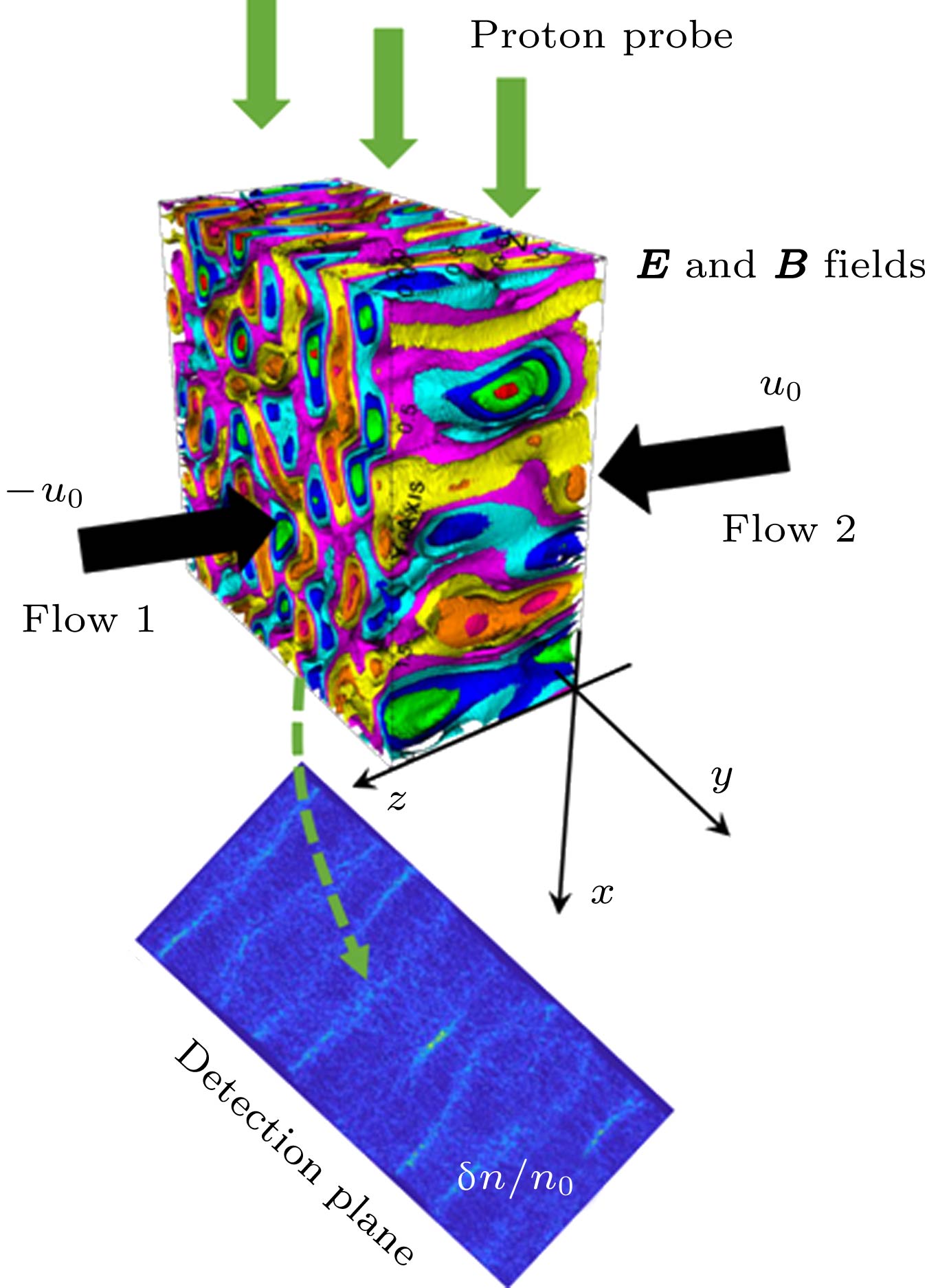
  • 图 1  Weibel不稳定性的质子照相示意图

    Fig. 1.  Schematic diagram of the proton radiography of the Weibel instability

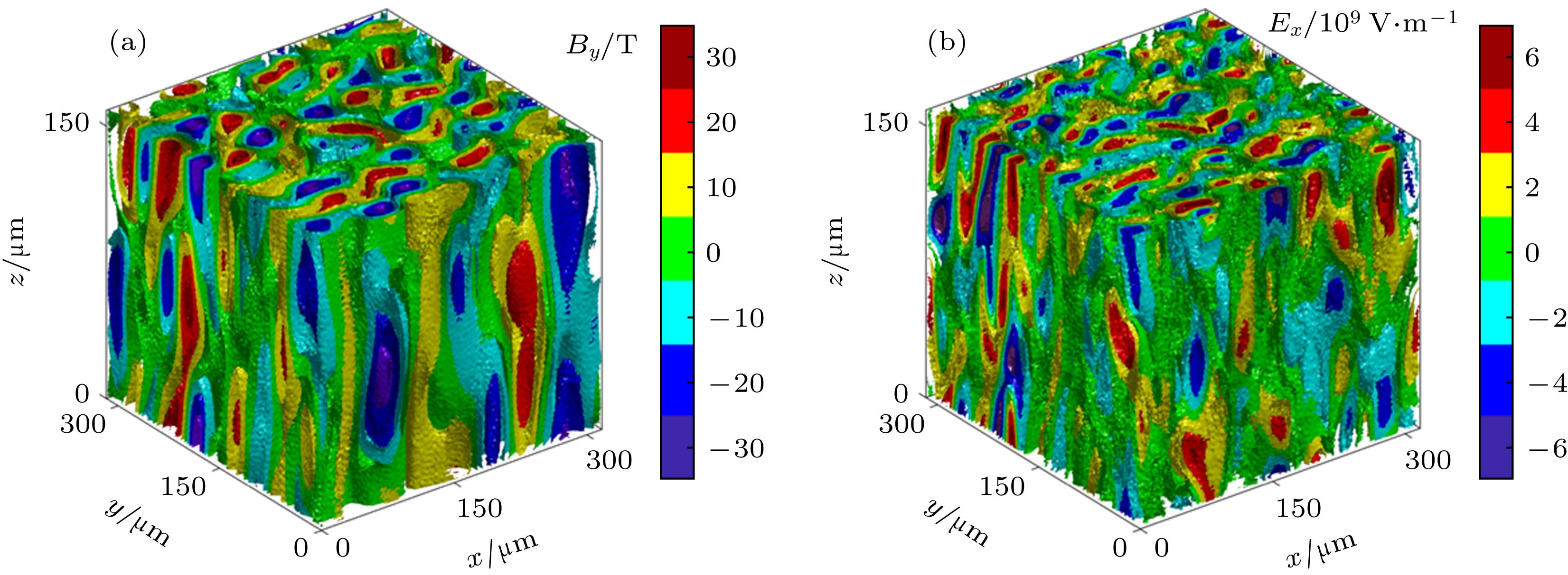
    图 2  Weibel不稳定性 (a)自生磁场By和(b)自生电场Ext = 1.06 ps时的三维空间分布

    Fig. 2.  Three demensional distributions of the Weibel instability generated (a) magnetic field By and (b) electric field Ex at t = 1.06 ps

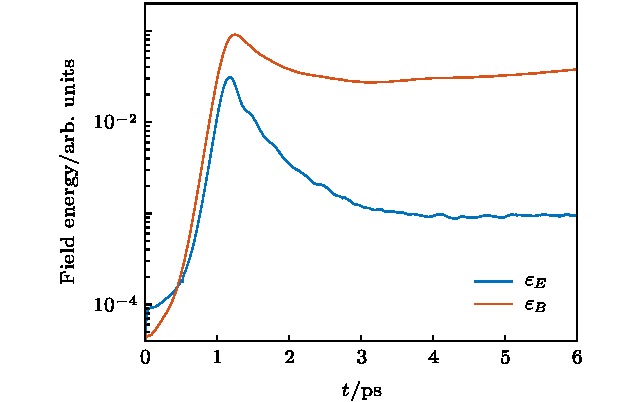
    图 3  Weibel不稳定性自生磁场和电场能量随着时间的演化

    Fig. 3.  Evolution of the energy of the Weibel instability generated magnetic and electric fields.

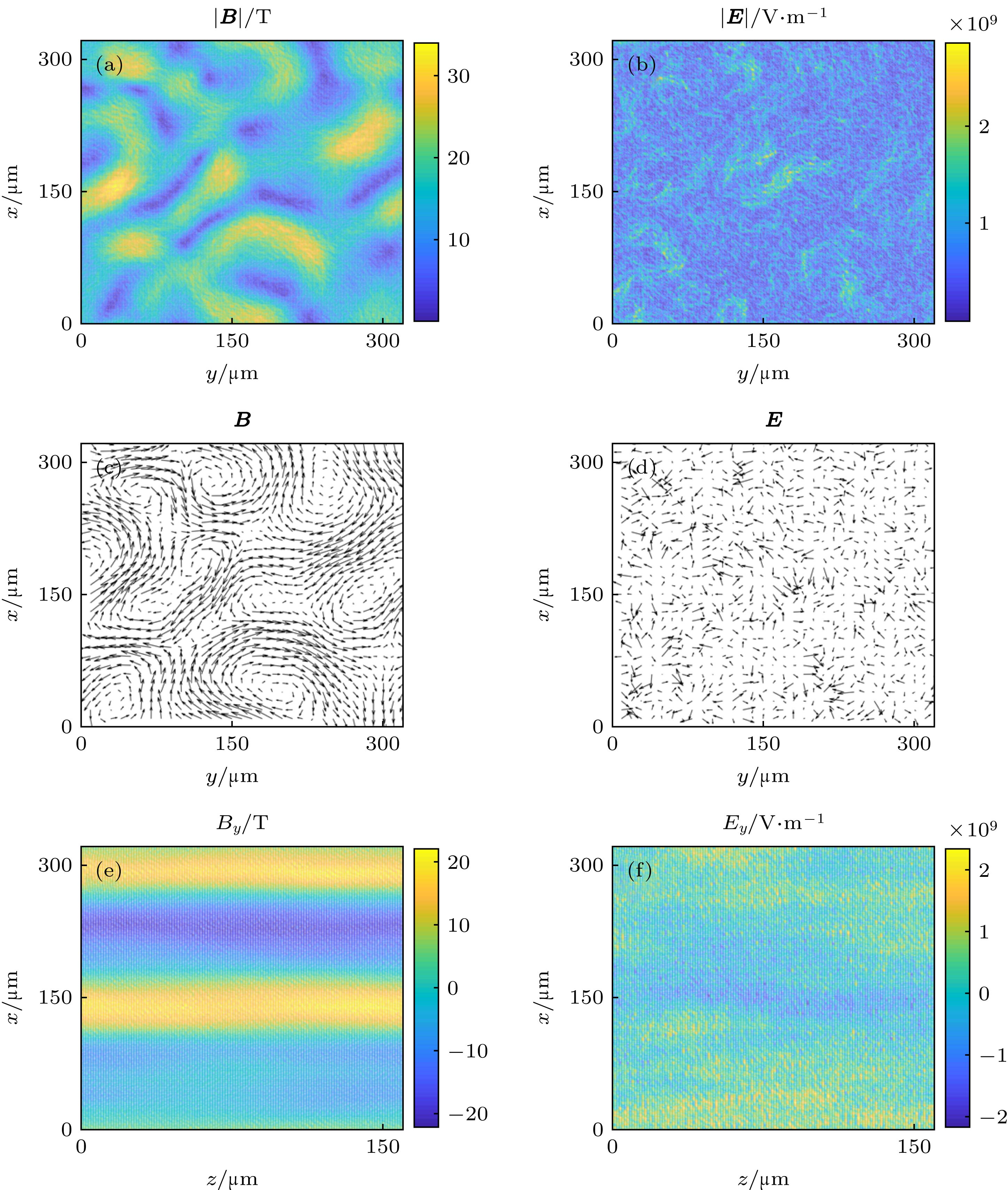
    图 4  t = 1.06 ps时, z = 0平面上(a)磁场强度|B|、(b)电场强度|E|、(c)磁场方向和(d)电场方向的分布情况以及y = 0平面上(e) y向磁场By和(f) y向电场Ey的分布情况

    Fig. 4.  Spatial distributions of (a) the magnetic field strength |B|, (b) the electric field strength |E|, (c) the direction of B and (d) the direction of E on the z = 0 plane, (e) the y component of the magnetic field By and (f) the y component of the electric field Ey on the y = 0 plane at t = 1.06 ps.

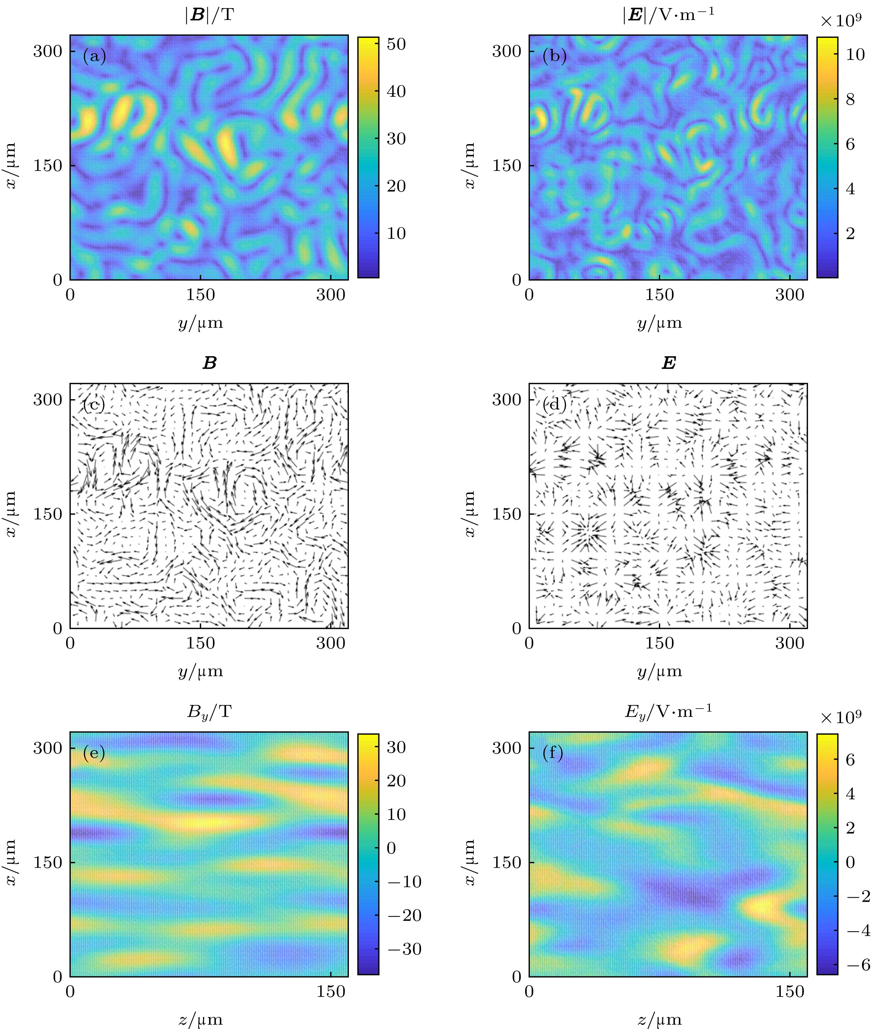
    图 5  t = 4.78 ps时, z = 0平面上(a)磁场强度|B|、(b)电场强度|E|、(c)磁场方向和(d)电场方向的分布情况以及y = 0平面上(e) y向磁场By和(f) y向电场Ey的分布情况

    Fig. 5.  Spatial distributions of (a) the magnetic field strength |B|, (b) the electric field strength |E|, (c) the direction of B and (d) the direction of E on the z = 0 plane, (e) the y component of the magnetic field By and (f) the y component of the electric field Ey on the y = 0 plane at t = 4.78 ps.

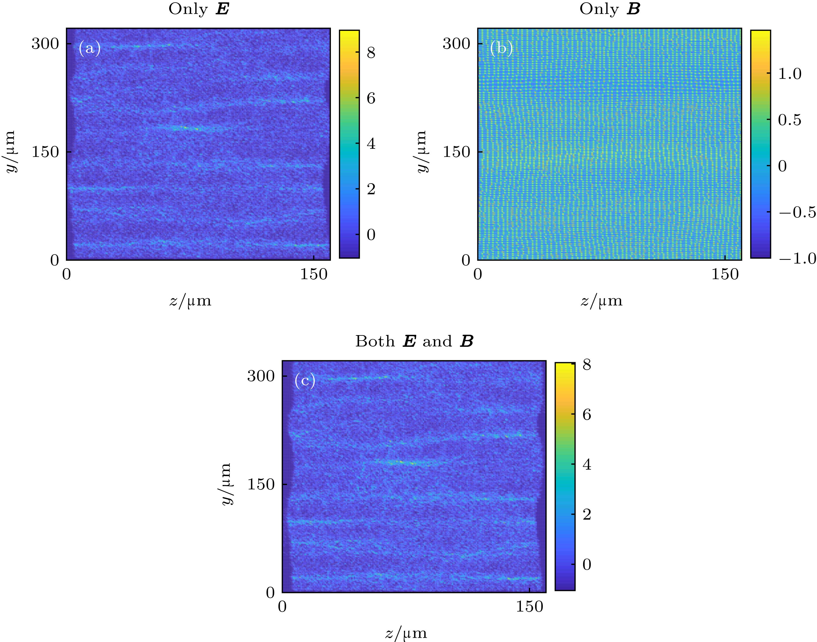
    图 6  t = 1.06 ps时, (a)只考虑电场E、(b)只考虑磁场B以及(c)同时考虑电场E和磁场B三种情况下探测面上的质子通量密度扰动分布信息

    Fig. 6.  Proton flux density perturbations on the detection plane when (a) only the electric field is included, (b) only the magnetic field is included and (c) both the electric and magnetic fields are included at t = 1.06 ps.

    图 7  t = 4.78 ps时(a)只考虑电场E、(b)只考虑磁场B以及(c)同时考虑电场E和磁场B三种情况下探测面上的质子通量密度扰动分布信息

    Fig. 7.  Proton flux density perturbations on the detection plane when (a) only the electric field is included, (b) only the magnetic field is included and (c) both the electric and magnetic fields are included at t = 4.78 ps.

  • [1]

    Weibel E S 1959 Phys. Rev. Lett. 2 83Google Scholar

    [2]

    Fried B D 1959 Phys. Fluids 2 337

    [3]

    Honda M, Meyer-ter-Vehn J, Pukhov A 2000 Phys. Rev. Lett. 85 2128Google Scholar

    [4]

    Ross J S, Park H S, Berger R, Divol L, Kugland N L, Rozmus W, Ryutov D, Glenzer S H 2013 Phys. Rev. Lett. 110 145005Google Scholar

    [5]

    Fiuza F, Fonseca R A, Tonge J, Mori W B, Silva L O1 2012 Phys. Rev. Lett. 108 235004Google Scholar

    [6]

    Ardaneh K, Cai D S, Nishikawa K I, Lembége B 2015 Astrophys. J. 811 57Google Scholar

    [7]

    Quinn K, Romagnani L, Ramakrishna B, Sarri G, Dieckmann M E, Wilson P A, Fuchs J, Lancia L, Pipahl A, Toncian T, Willi O, Clarke R J, Notley M, Macchi A, Borghesi M 2012 Phys. Rev. Lett. 108 135001Google Scholar

    [8]

    Kugland N L, Ryutov D D, Chang P Y, Drake R P, Fiksel G, Froula D H, Glenzer S H, Gregori G, Grosskopf M, Koenig M, Kuramitsu Y, Kuranz C, Levy M C, Liang E, Meinecke J, Miniati F, Morita T, Pelka A, Plechaty C, Presura R, Ravasio A, Remington B A, Reville B, Ross J S, Sakawa Y, Spitkovsky A, Takabe H, Park H S 2012 Nat. Phys. 8 809Google Scholar

    [9]

    Fox W, Fiksel G, Bhattacharjee A, Chang P Y, Germaschewski K, Hu S X, Nilson P M 2013 Phys. Rev. Lett. 111 225002Google Scholar

    [10]

    Huntington C M, Fiuza F, Ross J S, Zylstra A B, Drake R P, Froula D H, Gregori G, Kugland N L, Kuranz C C, Levy M C, Li C K, Meinecke J, Morita T, Petrasso R, Plechaty C, Remington B A, Ryutov D D, SakawaY, Spitkovsky A, Takabe H, Park S H 2015 Nat. Phys. 11 173Google Scholar

    [11]

    Tzoufras M, Ren C, Tsung F S, Tonge J W, Mori W B, Fiore M, Fonseca R A, Silva L O 2006 Phys. Rev. Lett. 96 105002Google Scholar

    [12]

    Dieckmann M E 2009 Plasma Phys. Control. Fusion 51 124042Google Scholar

    [13]

    Kugland N L, Ryutov D D, Plechaty C, Ross J S, Park H S 2012 Rev. Sci. Instruments 83 101301Google Scholar

    [14]

    Wang W W, Cai H B, Teng J, Chen J, He S K, Shan L Q, Lu F, Wu Y C, Zhang B, Hong W, Bi B, Zhang F, Liu D X, Xue F B, Li B Y, Liu H J, He W, Jiao J L, Dong K G, Zhang F Q, He Y L, Cui B, Xie N, Yuan Z Q, Tian C, Wang X D, Zhou K N, Deng Z G, Zhang Z M, Zhou W M, Cao L F, Zhang B H, Zhu S P, He X T, Gu Y Q 2018 Phys. Plasmas 25 083111Google Scholar

    [15]

    Bret A, Gremillet L, Dieckmann M E 2010 Phys. Plasmas 17 120501Google Scholar

    [16]

    Gao L, Nilson M P, Igumenshchev I V, Haines M G, Froula D H, Betti R, Meyerhofer D D 2015 Phys. Rev. Lett. 114 215003Google Scholar

    [17]

    Du B, Wang X F 2018 AIP Adv. 8 125328Google Scholar

    [18]

    Cai H B, Mima K, Zhou W M, Jozaki T, Nagatomo H, Sunahara A, Mason R J 2009 Phys. Rev. Lett. 102 245001Google Scholar

    [19]

    Cagas P, Hakim A, Scales W, Srinivasan B 2017 Phys. Plasmas 24 112116Google Scholar

    [20]

    Alves E P, Zrake J, Fiuza F 2018 Phys. Rev. Lett. 121 245101Google Scholar

    [21]

    Sentoku Y, Mima K, Sheng Z M, Kaw P, Nishihara K, Nishikawa K 2002 Phys. Rev. E 65 046408Google Scholar

    [22]

    Shukla C, Kumar A, Das A, Patel B G 2018 Phys. Plasmas 25 022123Google Scholar

    [23]

    Li C K, Séguin F H, Frenje J A, Rygg J R, Petrasso R D, Town R P J, Amendt P A, Hatchett S P, Landen O L, Mackinnon A J, Patel P K, Smalyuk V A, Sangster T C, Knauer J P 2006 Phys. Rev. Lett. 97 135003Google Scholar

    [24]

    Cecchetti C A, Borghesi M, Fuchs J, Schurtz G, Kar S, Macchi A, Romagnani, Wilson P A, Antici P, Jung R, Osterholtz J, Pipahl C, Willi O, Schiavi A, Notley M, Neely D 2009 Phys. Plasmas 16 043102Google Scholar

  • [1] 夏旭, 杨涓, 付瑜亮, 吴先明, 耿海, 胡展. 2 cm电子回旋共振离子推力器离子源中磁场对等离子体特性与壁面电流影响的数值模拟. 物理学报, 2021, 70(7): 075204. doi: 10.7498/aps.70.20201667
    [2] 杨思谦, 周维民, 王思明, 矫金龙, 张智猛, 曹磊峰, 谷渝秋, 张保汉. 通道靶对超强激光加速质子束的聚焦效应. 物理学报, 2017, 66(18): 184101. doi: 10.7498/aps.66.184101
    [3] 新波, 张小宁, 李韵, 崔万照, 张洪太, 李永东, 王洪广, 翟永贵, 刘纯亮. 多载波微放电阈值的粒子模拟及分析. 物理学报, 2017, 66(15): 157901. doi: 10.7498/aps.66.157901
    [4] 王洪广, 翟永贵, 李记肖, 李韵, 王瑞, 王新波, 崔万照, 李永东. 基于频域电磁场的微波器件微放电阈值快速粒子模拟. 物理学报, 2016, 65(23): 237901. doi: 10.7498/aps.65.237901
    [5] 何民卿, 董全力, 盛政明, 张杰. 激光驱动的冲击波自生磁场以及外加磁场的冲击波放大研究. 物理学报, 2015, 64(10): 105202. doi: 10.7498/aps.64.105202
    [6] 陈茂林, 夏广庆, 毛根旺. 多模式离子推力器栅极系统三维粒子模拟仿真. 物理学报, 2014, 63(18): 182901. doi: 10.7498/aps.63.182901
    [7] 陈兆权, 殷志祥, 陈明功, 刘明海, 徐公林, 胡业林, 夏广庆, 宋晓, 贾晓芬, 胡希伟. 负偏压离子鞘及气体压强影响表面波放电过程的粒子模拟. 物理学报, 2014, 63(9): 095205. doi: 10.7498/aps.63.095205
    [8] 董烨, 董志伟, 周前红, 杨温渊, 周海京. 沿面闪络流体模型电离参数粒子模拟确定方法. 物理学报, 2014, 63(6): 067901. doi: 10.7498/aps.63.067901
    [9] 陈再高, 王建国, 王玥, 乔海亮, 郭伟杰, 张殿辉. 基于粒子模拟和并行遗传算法的高功率微波源优化设计. 物理学报, 2013, 62(16): 168402. doi: 10.7498/aps.62.168402
    [10] 董烨, 董志伟, 杨温渊, 周前红, 周海京. 介质窗横向电磁场分布下的次级电子倍增效应. 物理学报, 2013, 62(19): 197901. doi: 10.7498/aps.62.197901
    [11] 王辉辉, 刘大刚, 蒙林, 刘腊群, 杨超, 彭凯, 夏蒙重. 气体电离的全三维电磁粒子模拟/蒙特卡罗数值研究. 物理学报, 2013, 62(1): 015207. doi: 10.7498/aps.62.015207
    [12] 邹德滨, 卓红斌, 邵福球, 银燕, 马燕云, 田成林, 徐涵, 欧阳建明, 谢翔云, 陈德鹏. 单束激光脉冲俘获及放大机理的理论分析与数值模拟研究. 物理学报, 2012, 61(4): 045202. doi: 10.7498/aps.61.045202
    [13] 郭帆, 李永东, 王洪广, 刘纯亮, 呼义翔, 张鹏飞, 马萌. Z箍缩装置外磁绝缘传输线全尺寸粒子模拟研究. 物理学报, 2011, 60(10): 102901. doi: 10.7498/aps.60.102901
    [14] 金晓林, 黄桃, 廖平, 杨中海. 电子回旋共振放电中电子与微波互作用特性的粒子模拟和蒙特卡罗碰撞模拟. 物理学报, 2009, 58(8): 5526-5531. doi: 10.7498/aps.58.5526
    [15] 巩华荣, 宫玉彬, 魏彦玉, 唐昌建, 薛东海, 王文祥. 考虑到束-波相互作用的速调管离子噪声二维模拟. 物理学报, 2006, 55(10): 5368-5374. doi: 10.7498/aps.55.5368
    [16] 卓红斌, 胡庆丰, 刘 杰, 迟利华, 张文勇. 超短脉冲激光与稀薄等离子体相互作用的准静态粒子模拟研究. 物理学报, 2005, 54(1): 197-201. doi: 10.7498/aps.54.197
    [17] 郑春阳, 刘占军, 李纪伟, 张爱清, 裴文兵. 无碰撞等离子体中电子束流不稳定性的时空演化研究. 物理学报, 2005, 54(5): 2138-2146. doi: 10.7498/aps.54.2138
    [18] 宫玉彬, 张 章, 魏彦玉, 孟凡宝, 范植开, 王文祥. 高功率微波器件中脉冲缩短现象的粒子模拟. 物理学报, 2004, 53(11): 3990-3995. doi: 10.7498/aps.53.3990
    [19] 盛政明, 张 杰, 余 玮. 强激光与等离子体相互作用中低频电磁场孤子波的产生及其捕获. 物理学报, 2003, 52(1): 125-134. doi: 10.7498/aps.52.125
    [20] 简广德, 董家齐. 环形等离子体中电子温度梯度不稳定性的粒子模拟. 物理学报, 2003, 52(7): 1656-1662. doi: 10.7498/aps.52.1656
计量
  • 文章访问数:  9093
  • PDF下载量:  78
出版历程
  • 收稿日期:  2019-05-21
  • 修回日期:  2019-07-03
  • 上网日期:  2019-09-01
  • 刊出日期:  2019-09-20

/

返回文章
返回