-
The topological transitions in two-dimensional photonic crystals (PCs) originate from the opening-closing-reopening of the bandgap, accompanied with the band order inversion. The topological bandgap in magnetic PC can be created by applying a bias magnetic field or deforming the geometry structure of the PC. In this paper, we demonstrate that the direction of the bias magnetic field also plays a key role in modifying the band structure in a two-dimensional magnetic PC. The results show that by reversing the direction of the bias magnetic field, the eigenstates with the same parity may exchange their orders in the band structure. We investigate this type of band order exchange in the applications of constructing topological edge states and its influence on the properties of edge states. We find, for example, reversing the direction of the bias magnetic field can create two almost degenerated topological edge modes, which propagate in the same direction but have opposite orbital angular momenta. The edge modes and their characteristics can be determined by the schematics of the band orders for the photonic crystals on the two sides of the boundary. The relative relationship of the band orders determines the emergence of the topological edge states, the number of edge states, and edge modes’ properties such as the orbital angular momentum and group velocity. Also, it affects the transmission efficiency of the electromagnetic wave on the boundary. The direction effect of the bias magnetic field on band order exchange presented in this paper provides us with a new way to change the feature of topological edge states and helps us to better understand the influence of band order on topological phases of photonic crystals. It may have potential applications, such as in pseudo-spin splitter and reflection-free one-way optical switch.
-
Keywords:
- magnetic photonic crystal /
- direction of bias magnetic field /
- topological band structure /
- edge state
[1] Ozawa T, Price H M, Amo A, Goldman N, Hafezi M, Lu L, Rechtsman M, Schuster D, Simon J, Zilberberg O 2019 Rev. Mod. Phys. 91 015006
 Google Scholar
[2] Raghu S, Haldane F D M 2008 Phys. Rev. Lett. 100 013904
 Google Scholar
[3] Haldane F D M, Raghu S 2008 Phys. Rev. A 78 033834
[4] Wang Z, Chong Y D, Joannopoulos J D, Soljačić M 2008 Phys. Rev. Lett. 100 013905
 Google Scholar
[5] Wang Z, Chong Y D, Joannopoulos J D, Soljačić M 2009 Nature 461 772
 Google Scholar
[6] Lu L, Joannopoulos J D, Soljačić M 2014 Nat. Photonics 8 821
 Google Scholar
[7] Qiu W, Wang Z, Soljačić M 2011 Opt. Express 19 22248
 Google Scholar
[8] He C, Chen X L, Lu M H, Li X F, Wan W W, Qian X S, Yin R C, Chen Y F 2010 Appl. Phys. Lett. 96 111111
 Google Scholar
[9] Yang Y, Poo Y, Wu R X, Gu Y, Chen P 2013 Appl. Phys. Lett. 102 231113
 Google Scholar
[10] Wu Y, Li C, Hu X, Ao Y, Zhao Y, Gong Q 2017 Adv. Opt. Mater. 5 1700357
 Google Scholar
[11] Poo Y, Wu R X, Lin Z F, Yang Y, Chan C T 2011 Phys. Rev. Lett. 106 093903
 Google Scholar
[12] Wu L H, Hu X 2015 Phys. Rev. Lett. 114 223901
 Google Scholar
[13] Yang Y, Xu Y F, Xu T, Wang H X, Jiang J H, Hu X, Hang Z H 2018 Phys. Rev. Lett. 120 217401
 Google Scholar
[14] Xu L, Wang H X, Xu Y D, Chen H Y, Jiang J H 2016 Opt. Express 24 18059
 Google Scholar
[15] Zhu X, Wang H X, Xu C, Lai Y, Jiang J H, John S 2018 Phys. Rev. B 97 085148
 Google Scholar
[16] Chen Z G, Mei J, Sun X C, Zhang X, Zhao J, Wu Y 2017 Phys. Rev. A 95 043827
 Google Scholar
[17] Gao Z, Yang Z, Gao F, Xue H, Yang Y, Dong J, Zhang B 2017 Phys. Rev. B 96 201402
 Google Scholar
[18] Ma T, Shvets G 2016 New J. Phys. 18 025012
 Google Scholar
[19] Gao F, Xue H, Yang Z, Lai K, Yu Y, Lin X, Chong Y, Shvets G, Zhang B 2017 Nat. Phys. 14 140
[20] Chen X D, Zhao F L, Chen M, Dong J W 2017 Phys. Rev. B 96 020202
 Google Scholar
[21] He X T, Liang E T, Yuan J J, Qiu H Y, Chen X D, Zhao F L, Dong J W 2019 Nat. Commun. 10 872
 Google Scholar
[22] Zhang L, Yang Y H, He M J, Wang H X, Yang Z J, Li E P, Gao F, Zhang B L, Singh R J, Jiang J H, Chen H S 2019 Laser Photonics Rev. 13 1900159
 Google Scholar
[23] Lu J C, Chen X D, Deng W M, Chen M, Dong J W 2018 J. Opt. 20 075103
 Google Scholar
[24] Chan H C, Guo G Y 2018 Phys. Rev. B 97 045422
 Google Scholar
[25] Pozar D M 2012 Microwave Engineering (Hoboken: John Wiley & Sons) pp451–465
[26] Xi X, Lin M, Qiu W, Ouyang Z, Wang Q, Liu Q 2018 Sci. Rep. 8 7827
 Google Scholar
[27] Qi X L, Wu Y S, Zhang S C 2006 Phys. Rev. B 74 045125
 Google Scholar
[28] Ju C, Wu R X, Li Z, Poo Y, Liu S Y, Lin Z F 2017 Opt. Express 25 22096
 Google Scholar
-
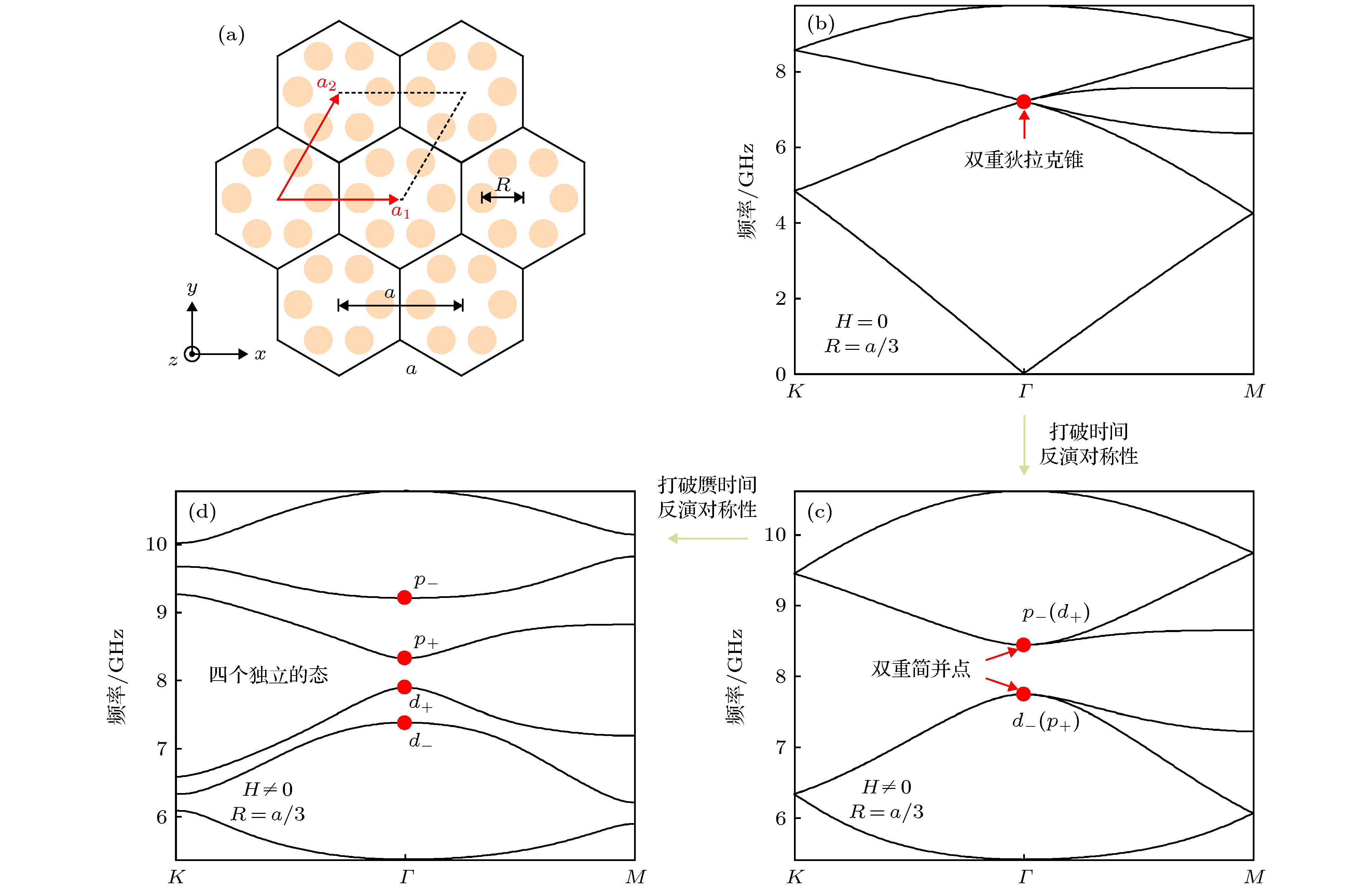
图 1 (a)二维光子晶体示意图, 其中黄色的圆表示空气背景中的铁氧体柱, 黑色六边形表示阵列结果中的一个基元; (b) H = 0和R = a/3时的能带结构, 在Γ点具有一个四重简并点; (c) H ≠ 0和R = a/3时的能带结构(由于打破时间反演对称性, 能带结构中出现了完全带隙, 并在Γ点出现了两个双重简并点); (d) H ≠ 0和R ≠ a/3时的能带结构
Fig. 1. (a) Schematic of two-dimensional magnetic photonic crystal fabricated by ferrite rods (denoted by yellow circles) embedded in air background. The black hexagon denotes the basis of the array. (b) Band structure at H = 0 and R = a/3. A four-fold degeneracy point shows at the Γ point. (c) Band structure at H ≠ 0 and R = a/3. A full bandgap presents in the band structure because of time reverse symmetry broken, and two doubly degeneracy points present at Γ point. (d) Band structure at H ≠ 0 and R ≠ a/3.
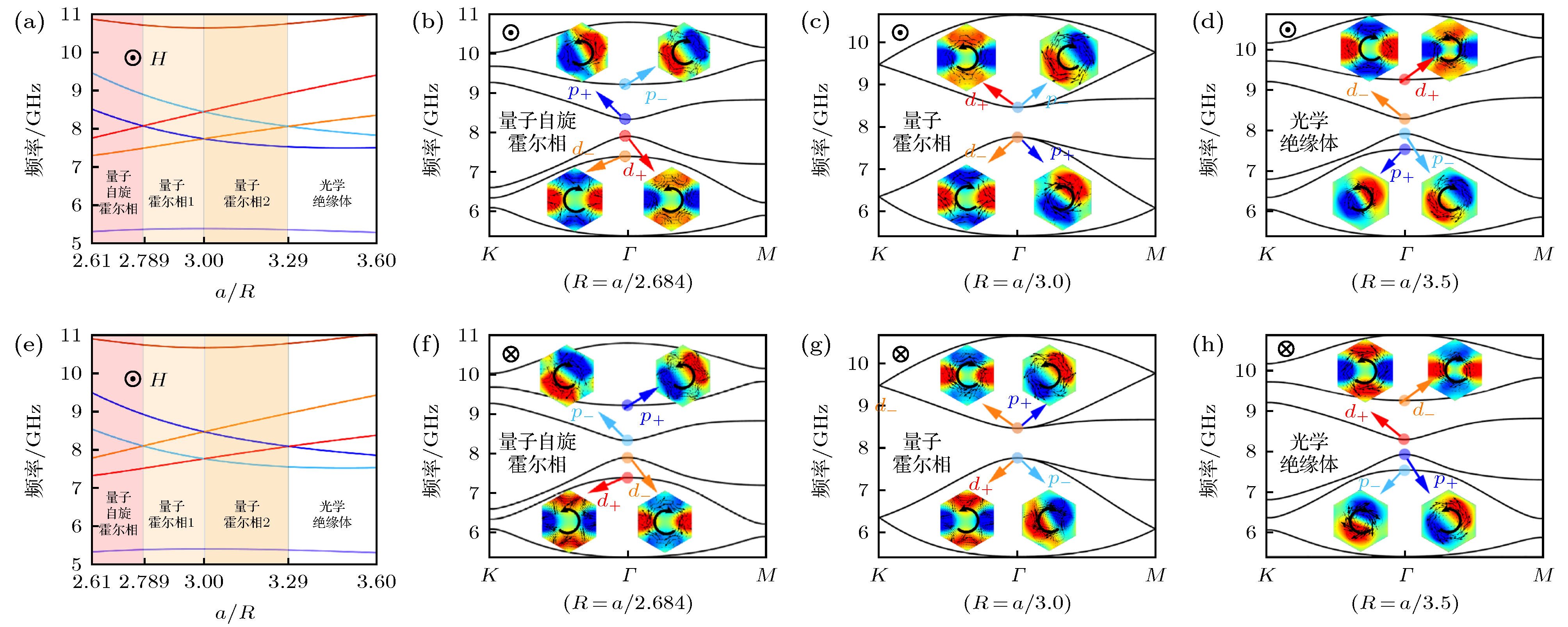
图 2 正向和反向偏置磁场时, Г点处四个本征态的电场相位分布和磁场(反转偏置磁场的方向将使得本征态的电场相位和磁场在形式上出现p+和p-, d+和d-之间的交换)
Fig. 2. Magnetic fields and the phase of electric fields for the eigenstates p+, p-, d+, d- at the Г point. Reversing the direction of bias magnetic field causes the exchange in the profiles of electric phase and magnetic field.
图 3 (a)当偏置磁场沿着+z方向时, Г点的p态和d态的本征频率随参数a/R的变化(随着a/R的增加, Г点处发生能带带序反转, 并伴随着拓扑相变; 不同颜色的阴影显示三种不同的拓扑相); (b)−(d)分别是当光子晶体处于量子自旋霍尔相(R = a/2.684)、量子霍尔相(R = a/3)和光学绝缘相(R = a/3.5)时的能带结构; 图中的插图是能带结构对应点上的场模式图, 其中黑色箭头表示坡印亭矢量; (e)−(h)是当偏置磁场沿着–z方向时, 本征频率随a/R的变化, 以及三种典型的拓扑相的能带结构和场模式
Fig. 3. (a) Evolution of p and d eigenstates at point Г as a function of the radio of a/R with the bias magnetic field in the +z direction. As a/R increases, the band order exchange takes place where phase transition happens. Three types of phases are shaded in different colors. (b)−(d) Typical band structures of quantum spin-Hall (QSH) phase (R = a/2.684), quantum Hall (QH) phases (R = a/3), and conventional insulator (CI) phase (R = a/3.5). (e)−(h) The same as (a)−(d), but the bias magnetic field is in the –z direction. The insets of the panels (b)−(d) and (f)−(g) are the profile of eigenstates at the corresponding dots on the band structure of the panels, where the black arrow indicates the Poynting vectors.
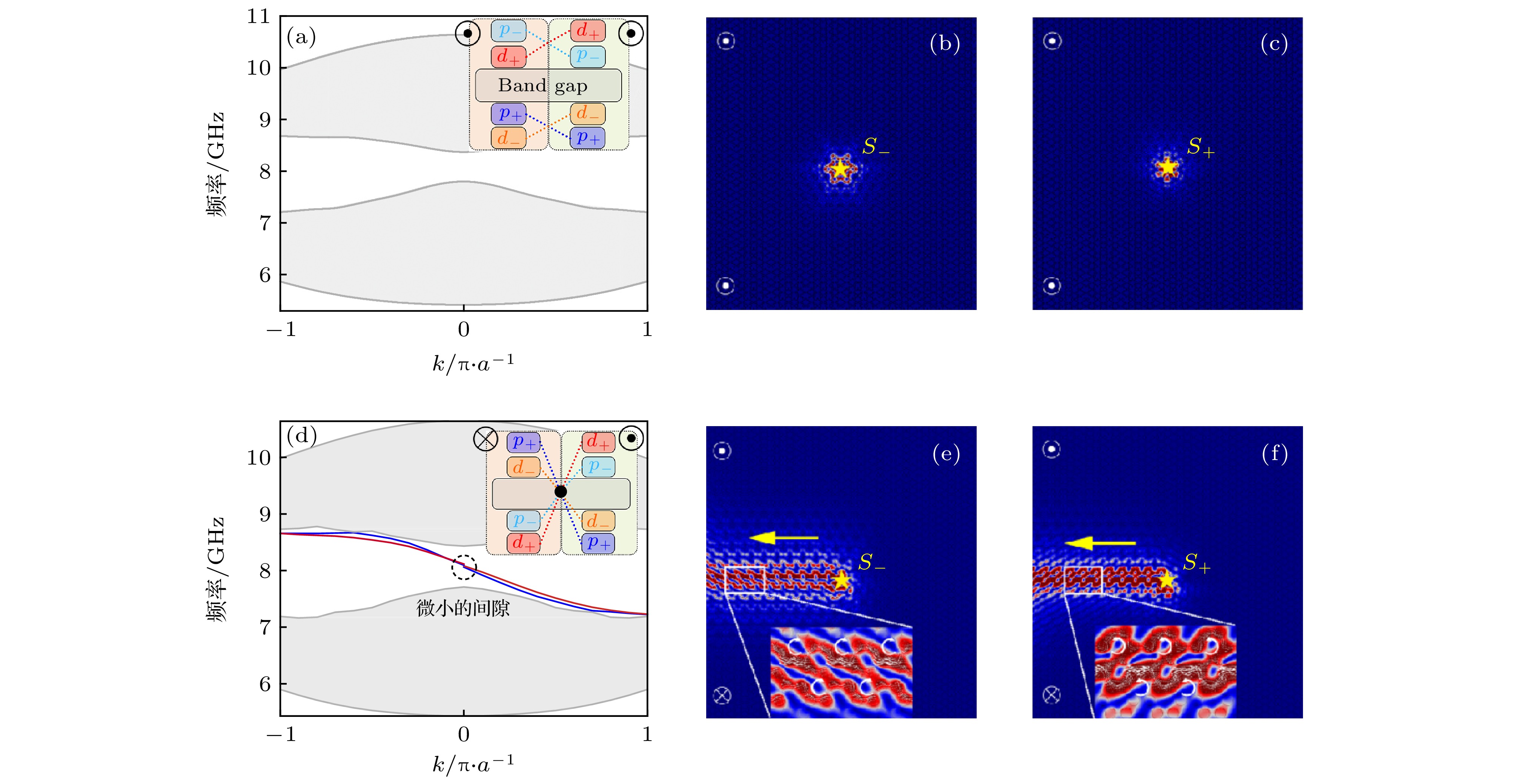
图 4 偏置磁场方向对边界态的影响(区域I和II均处于量子霍尔相, 但结构参量R分别是a/2.93和a/3.09) (a)两个区域施加同向偏置磁场时的投影能带结构; (b)和(c)分别用激发源S+和S–激发时的场分布; (d)两个区域施加反向偏置磁场时的投影能带结构; (e)和(f)分别用激发源S+和S–激发时的场分布, 其中的放大图展示了电磁波的轨道角动量特性, 图中箭头表示坡印亭矢量(当两个区域施加反向偏置磁场时, S+和S–都可以激发沿同一方向传播的单向波); (a)和(d)图中的插图给出了两个区域中能带结构的对应关系, 两块域中相同的本征态连线连的交叉点出现在共同带隙中时将出现拓扑边界态
Fig. 4. Influence of the direction of bias magnetic field on the edge states when two domains are in the QH phase but have different geometric structure (R = a/2.93 and R = a/3.09). (a) The projected band structure when two domains are applied by the same direction of bias magnetic field. (b) and (c) Electrical field distribution at 8 GHz excited by S+ and S–, respectively. No edge mode is excited. (d) The projected band structure when two domains are applied by the opposite direction of bias magnetic field. (e) and (f) Electric field distribution corresponding to (d) at 8 GHz excited by S+ and S–. The waves propagate unidirectional. The inset enlarges the field details which shows the orbital angular momentum of the wave. The inserts of (a) and (d) show the schematic of the relationship of the topological edge state and eigenstates in the two domains.
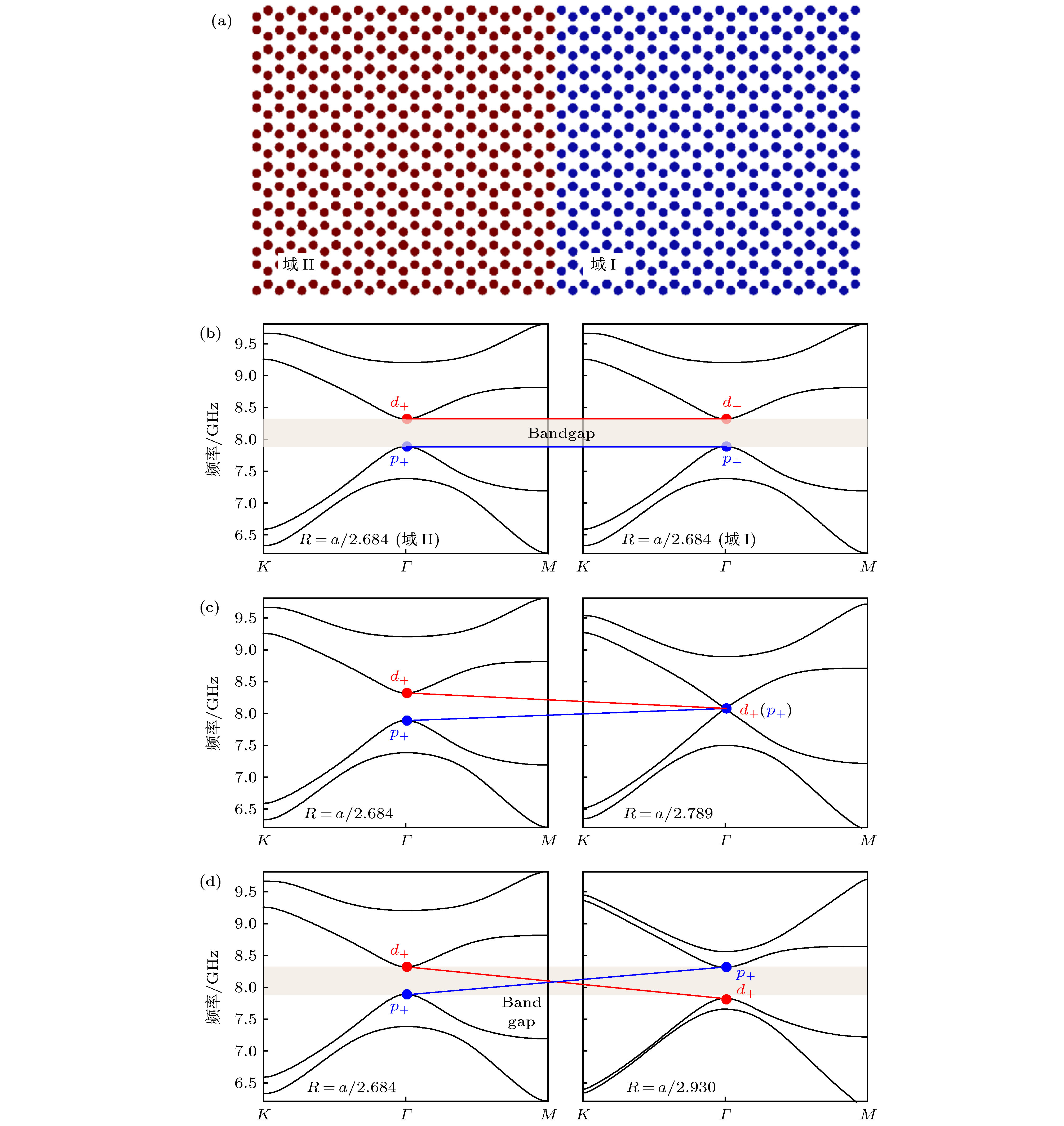
图 5 (a)由两个具有不同拓扑指数的域组合在一起形成的域边界(假设保持域II固定在量子自旋霍尔相); (b)−(d)域I从量子自旋霍尔相转变到量子霍尔相时, 域边界出现拓扑边界态的过程示意图
Fig. 5. (a) Schematics of the domain boundary created by two domains with distinct topological index. Supposing the domain II keeps in QSH phase. (b)−(d) The procedure of the topological edge state creation when domain I takes place the phase transiting from QSH phase to QH phase.
图 6 区域I和II分别处于量子自旋霍尔相和量子霍尔相时, 偏置磁场方向对边界态的影响 (a)同向偏置磁场和(b)正反向偏置磁场时的投影能带结构(两条边界态具有相反的群速度和轨道角动量, 在边界上形成与量子自旋霍尔效应相似的赝自旋单向波; 采用正反向偏置磁场可以有效地减小边界态的间隙); (c) S+激发源可以实现向左边传播的单向传播; (d) S–激发源可以实现向右边传播的单向传播; (e)当S被激发时, TE波沿着两个方向传播
Fig. 6. Influence of the direction of bias magnetic field on the edge states when two domains are the QSH phase and the CI phases, respectively. (a), (b) The projected band structure for the two domains are respectively applied by the same and the opposite direction of bias magnetic field. The edge states localized at the boundary lead to a pseudo-spin dependent one-way propagation. The application of using opposite direction of bias magnetic field in the two domain reduces the gap of edge states. (c) Unidirectional wave propagation localized at domain interface excited by S+. (d) Unidirectional wave propagation excited by S–. (e) TE wave propagates along with opposite side when it is excited by S.
图 7 (a)传输效率计算示意图; (b)与图6对应的传输效率(红线和蓝线相应于边界两侧同向和正反向偏置磁场时边界态的传输效率, 绿线和黑线是左侧光子晶体(R = a/2.684)和右侧光子晶体(R = a/3.5)单独存在时的传输效率, 阴影区为两侧光子晶体的共同带隙)
Fig. 7. (a) Schematic of the computational transmission efficiency. (b) The transmission efficiency corresponding to the Fig. 6. The transmission efficiency of the edge state under the condition of applying bias magnetic field with the same (red curve) or opposite direction (blue curve) in the two domains. The transmission efficiency of the full photonic crystals of the left domain is shown in green curve and the right domain in black curve. The shadow region indicates the common band gaps.
表 1 由本征态连接方式决定边界态的轨道角动量和群速度
Table 1. Orbital angular momentums and group velocities determined by the linked manner of eigenstates.
本征态 连接方式 轨道角动量 群速度 d+ 从左下方到右上方 正 负 p+ 从左上方到右下方 p– 从左下方到右上方 负 负 d– 从左上方到右下方 d– 从左下方到右上方 负 正 p– 从左上方到右下方 p+ 从左下方到右上方 正 正 d+ 从左上方到右下方 -
[1] Ozawa T, Price H M, Amo A, Goldman N, Hafezi M, Lu L, Rechtsman M, Schuster D, Simon J, Zilberberg O 2019 Rev. Mod. Phys. 91 015006
 Google Scholar
[2] Raghu S, Haldane F D M 2008 Phys. Rev. Lett. 100 013904
 Google Scholar
[3] Haldane F D M, Raghu S 2008 Phys. Rev. A 78 033834
[4] Wang Z, Chong Y D, Joannopoulos J D, Soljačić M 2008 Phys. Rev. Lett. 100 013905
 Google Scholar
[5] Wang Z, Chong Y D, Joannopoulos J D, Soljačić M 2009 Nature 461 772
 Google Scholar
[6] Lu L, Joannopoulos J D, Soljačić M 2014 Nat. Photonics 8 821
 Google Scholar
[7] Qiu W, Wang Z, Soljačić M 2011 Opt. Express 19 22248
 Google Scholar
[8] He C, Chen X L, Lu M H, Li X F, Wan W W, Qian X S, Yin R C, Chen Y F 2010 Appl. Phys. Lett. 96 111111
 Google Scholar
[9] Yang Y, Poo Y, Wu R X, Gu Y, Chen P 2013 Appl. Phys. Lett. 102 231113
 Google Scholar
[10] Wu Y, Li C, Hu X, Ao Y, Zhao Y, Gong Q 2017 Adv. Opt. Mater. 5 1700357
 Google Scholar
[11] Poo Y, Wu R X, Lin Z F, Yang Y, Chan C T 2011 Phys. Rev. Lett. 106 093903
 Google Scholar
[12] Wu L H, Hu X 2015 Phys. Rev. Lett. 114 223901
 Google Scholar
[13] Yang Y, Xu Y F, Xu T, Wang H X, Jiang J H, Hu X, Hang Z H 2018 Phys. Rev. Lett. 120 217401
 Google Scholar
[14] Xu L, Wang H X, Xu Y D, Chen H Y, Jiang J H 2016 Opt. Express 24 18059
 Google Scholar
[15] Zhu X, Wang H X, Xu C, Lai Y, Jiang J H, John S 2018 Phys. Rev. B 97 085148
 Google Scholar
[16] Chen Z G, Mei J, Sun X C, Zhang X, Zhao J, Wu Y 2017 Phys. Rev. A 95 043827
 Google Scholar
[17] Gao Z, Yang Z, Gao F, Xue H, Yang Y, Dong J, Zhang B 2017 Phys. Rev. B 96 201402
 Google Scholar
[18] Ma T, Shvets G 2016 New J. Phys. 18 025012
 Google Scholar
[19] Gao F, Xue H, Yang Z, Lai K, Yu Y, Lin X, Chong Y, Shvets G, Zhang B 2017 Nat. Phys. 14 140
[20] Chen X D, Zhao F L, Chen M, Dong J W 2017 Phys. Rev. B 96 020202
 Google Scholar
[21] He X T, Liang E T, Yuan J J, Qiu H Y, Chen X D, Zhao F L, Dong J W 2019 Nat. Commun. 10 872
 Google Scholar
[22] Zhang L, Yang Y H, He M J, Wang H X, Yang Z J, Li E P, Gao F, Zhang B L, Singh R J, Jiang J H, Chen H S 2019 Laser Photonics Rev. 13 1900159
 Google Scholar
[23] Lu J C, Chen X D, Deng W M, Chen M, Dong J W 2018 J. Opt. 20 075103
 Google Scholar
[24] Chan H C, Guo G Y 2018 Phys. Rev. B 97 045422
 Google Scholar
[25] Pozar D M 2012 Microwave Engineering (Hoboken: John Wiley & Sons) pp451–465
[26] Xi X, Lin M, Qiu W, Ouyang Z, Wang Q, Liu Q 2018 Sci. Rep. 8 7827
 Google Scholar
[27] Qi X L, Wu Y S, Zhang S C 2006 Phys. Rev. B 74 045125
 Google Scholar
[28] Ju C, Wu R X, Li Z, Poo Y, Liu S Y, Lin Z F 2017 Opt. Express 25 22096
 Google Scholar
计量
- 文章访问数: 13261
- PDF下载量: 485
- 被引次数: 0


 下载:
下载:


