


-
本工作应用截面扫描隧道显微镜(XSTM)研究了In0.53Ga0.47As/InP异质结构的(110)解理面. 扫描隧道谱(STS)测量结果显示, InGaAs的电流-电压(I-V)隧道谱呈现与衬底InP(110)面完全不同特点. InP的I-V谱呈现的零电流平台宽度(隧道谱表观带隙)接近材料带隙, 可基于平带模型解释. In0.53Ga0.47As的表观带隙却比其带隙(室温0.74 eV)高出约50%. 这反映了针尖与InGaAs发生隧穿时的不同物理图像, 需应用针尖诱导能带弯曲(TIBB)模型来解释. 基于三维TIBB模型的计算, 我们发现表面态密度是对隧道谱线特征具有敏感影响的参数. 适当选取参数不仅能定量解释InGaAs的I-V谱的零电流平台宽度, 而且能较准确预言零电流平台的起、止能量位置,并能计算给出与实验高度重合的I-V理论谱线.The cross-sectional (110) surface of In0.53Ga0.47As/InP hetero-structure grown by molecular beam epitaxy on an InP (001) substrate is characterized by the cross-sectional scanning tunneling microscopy (XSTM). The cleaved (110) surface across the interface between the In0.53Ga0.47As layer and InP layer is atomically flat but displays slight different image contrast between the two neighbor regions. The scanning tunneling spectroscopy (STS) is used to measure the current/voltage (I-V) spectra. The I-V data of the InGaAs surface and InP (110) surface show the different characteristics. The voltage range of zero-current plateau (apparent band gap) in the I-V spectrum of InP displays the values close to its energy band gaps whereas the plateau ranges in the spectra of In0.53Ga0.47As are by contrast generally 50% larger than the energy band gap of In0.53Ga0.47As. The above phenomenon implies the different physical pictures on the tunneling of two surfaces. In the case of InP, the flat band model is feasible since the band edge states existing in the InP (110) surface can prevent the surface from being affected by the tip –induced band bending (TIBB) effect. In contrast, the TIBB effect must be taken into account to explain the I-V spectra of the In0.53Ga0.47As (110) surface. A statistical analysis of the I-V data of In0.53Ga0.47As reveals that the width of current plateau in the I-V spectrum is generally between 1.05 eV and 1.20 eV and the current onset points (turn-points) with the plateau for the different spectra are slightly different from each other. We are able to explain quantitatively the above features based on the three-dimensional TIBB model given by Feenstra (
2003 J. Vac. Sci. Technol. B 21 2080 ). Our calculation reveals that the parameter of density of surface states (DOSS) is a sensitive parameter responsible for the I-V features mentioned above. According to an appropriate assignment of the value of DOSS, which is generally taken in the scope of (0.8–3.0) × 1012 (cm2·eV)–1, we well predict both the width and the onset points of the current-plateau. Moreover, the model also reproduces the line-shapes of the I-V spectra measured on In0.53Ga0.47As.-
Keywords:
- semiconductor surface /
- scanning tunneling microscopy /
- scanning tunneling spectroscopy /
- tip-induced band bending
[1] Tian Z, Gan Y, Zhang T, Wang B, Ji H, Feng Y, Xue J 2019 Phys. Rev. B 100 085440
 Google Scholar
[2] Lee D H, Gupta J A 2010 Science 330 1807
Google Scholar
[3] Wijnheijmer A P, Garleff J K, Teichmann K, Wenderoth M, Loth S, Ulbrich R G, Maksym P A, Roy M, Koenraad P M 2009 Phys. Rev. Lett. 102 166101
Google Scholar
[4] Timm R, Feenstra R M, Eisele H, Lenz A, Ivanova L, Lenz E, and Dähne M 2009 J. Appl. Phys 105 093718
Google Scholar
[5] Huang B C, Chiu Y P, Huang P C, Wang W C, Tra V T, Yang J C, He Q, Lin J Y, Chang C S, Chu Y H 2012 Phys. Rev. lett. 109 246807
Google Scholar
[6] Lin H, Lagoute J, Repain V, Chacon C, Girard Y, Lauret J -S, Ducastelle F, Loiseau A, Rousset S 2010 Nat. Mater. 9 235
Google Scholar
[7] Shao F, Zha F X, Pan B C, Shao J, Zhao X L, Shen X C 2014 Phys. Rev. B 89 085423
Google Scholar
[8] Feenstra R M 2003 J. Vac. Sci. Technol. B 21 2080
Google Scholar
[9] Feenstra R M 2009 Surf. Sci. 603 2841
Google Scholar
[10] Feenstra R M, Gaan S, Meyer G, Rieder K H 2005 Phys. Rev. B 71 125316
Google Scholar
[11] Dong Y, Feenstra R M, Semtsiv M P, Masselink W T 2008 J. Appl. Phys. 103 073704
Google Scholar
[12] Ishida N, Sueoka K, Feenstra R M 2009 Phys. Rev. B 80 075320
Google Scholar
[13] Rouvié A, Coussement J, Huet O, Truffer JP, Pozzi M, Oubensaid E H, Hamard S, Maillart P, Costard E 2014 Proc. of SPIE 9249 92490Z
Google Scholar
[14] Wen J, Wang W J, Chen X R, Li N, Chen X S, Lu W 2018 J. Appl. Phys. 123 161530
Google Scholar
[15] 郑文龙, 张亚光, 顾溢, 李宝宝, 陈泽中, 陈平平 2019 红外与毫米波学报 38 1001
Zheng W L, Zhang Y G, Gu Y, Li B B, Chen Z Z, Chen P P 2019 J. Infrared Millim. Waves 38 1001
[16] Zha F X, Hong F, Pan B C, Wang Y, Shao J, Shen X C 2018 Phys. Rev. B 97 035401
Google Scholar
[17] Mikkelsen A, Lundgren E 2005 Prog. Surf. Sci. 80 1
Google Scholar
[18] Feenstra R M 1994 Phys. Rev. B 50 4561
Google Scholar
[19] Albrektsen O, Arent D J, Meier H P, Salemink H W M, 1990 Appl. Phys. Lett. 57 31
Google Scholar
[20] Newman N, Spicer W E, Kendelewicz T, Lindau I 1986 J. Vac. Sci. Technol. B 4 931
Google Scholar
[21] 邓宗武, 郭伟民, 刘焕明, 曹立礼 1999 物理化学学报 15 303
Google Scholar
Deng Z W, Kwok Raymund W M, Lau Leo W M, Cao L L 1999 Acta Phys-Chim. Sin. 15 303
Google Scholar
[22] Kingston R H, Neustadter S F 1955 J. Appl. Phys 26 718
Google Scholar
[23] Seiwatz R, Green M 1958 J. Appl. Phys 29 1034
Google Scholar
[24] Jäger N D, Weber E R, Urban K, Ebert P H 2003 Phys. Rev. B 67 165327
Google Scholar
[25] Ivanova L, Borisova S, Eisele H, Dähne M, Laubsch A, Ebert P H 2008 Appl. Phys. Lett. 93 192110
Google Scholar
-
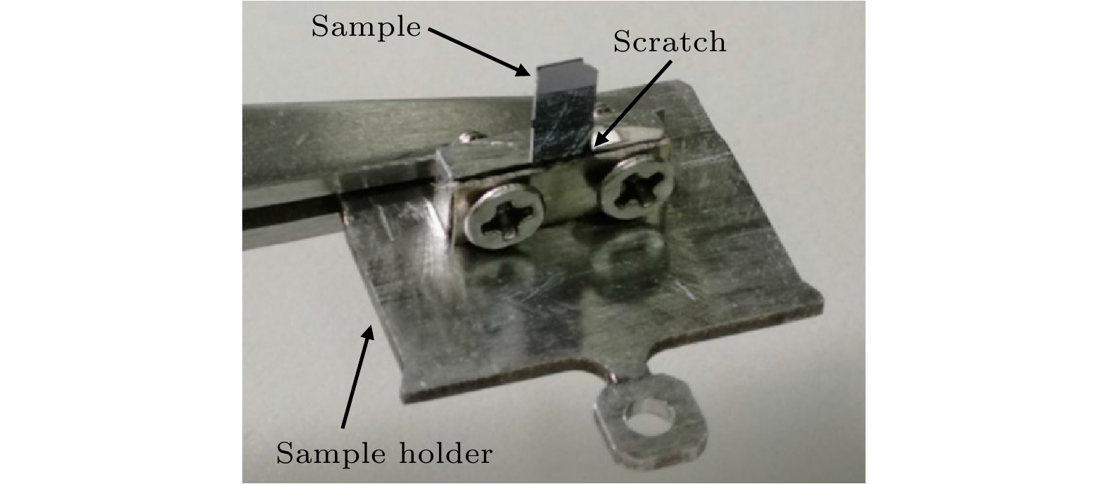
图 1 处于样品托中用于XSTM实验的样品照片
Fig. 1. Photography of sample in the sample holder for the XSTM experiment.

图 2 (a) InGaAs/InP异质结(110)解理面的STM形貌; (b)和(c)为InP和InGaAs(110)面的典型的I-V隧道谱给出的表观带隙测量结果; (d)和(e)分别为在InP和InGaAs(110)表面分别随机采样13和17条I-V谱线给出的表观带隙直方图统计结果
Fig. 2. (a) STM topography of the cleaved (110) surface of InGaAs/InP hetero-structure; (b) and (c) are the typical I-V tunneling spectra of InP and InGaAs (110) surface, respectively; (d) and (e) are the statistical histograms of the apparent tunneling gaps with the sampling of 13 and 17 spectra on the (110) surfaces, respectively.
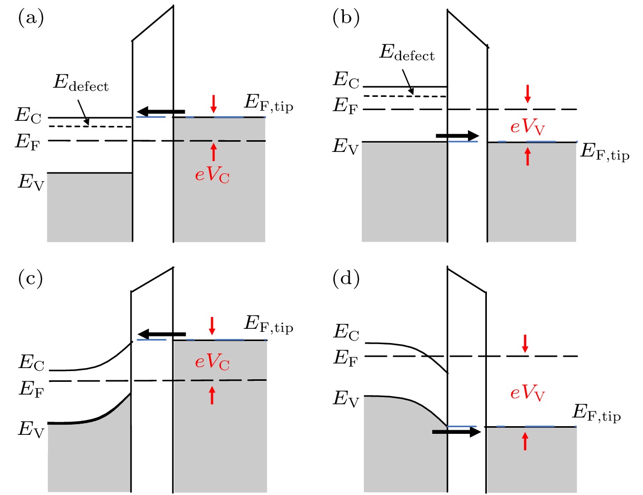
图 3 平带模型的STM隧道结能带示意图 (a)正偏压; (b)负偏压; TIBB模型下的隧穿能带图 (c)正偏压; (d)负偏压.EC, EV和EF分别是样品的导带、价带和费米能级, EF, tip是针尖的费米能级, Edefect表示缺陷态能级.
Fig. 3. Schematic energy band diagram of STM tunneling junction with flat band model: (a) Positive sample bias; (b) negative sample bias; schematic energy band diagram of tunneling junction with the TIBB model: (c) positive sample bias; (d) negative sample bias. EC, EV and EF are the conduction band, valence band and Fermi level of the sample respectively, EF, tip is the Fermi level of the tip, and Edefect is the defect level.
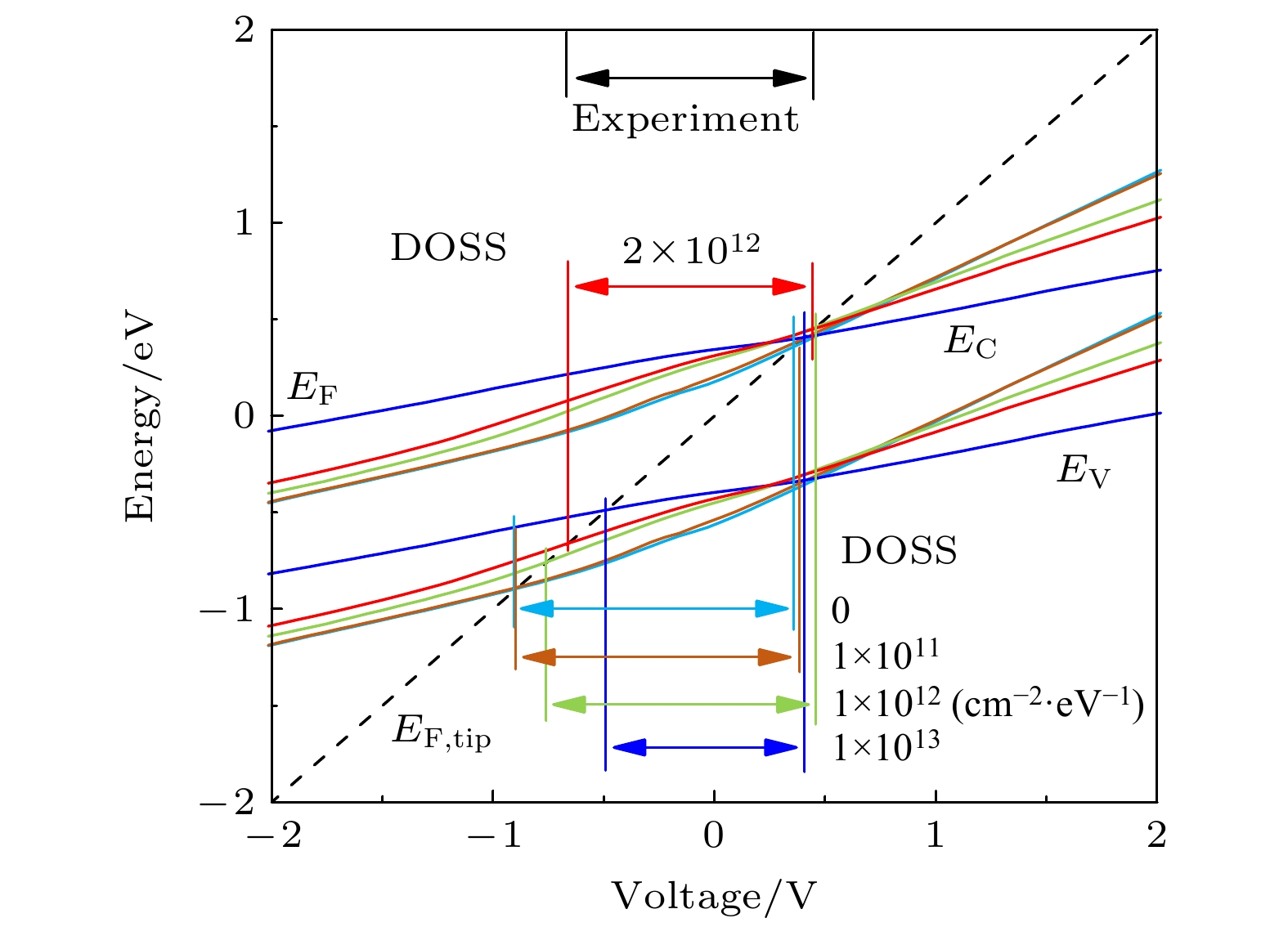
图 4 三维TIBB模型给出的InGaAs表面处带边电势能随所加样品偏压的变化关系, 不同颜色的实线对应于不同DOSS, 对应箭头所指为该态密度下计算得到的表观带隙, 优化的DOSS对应计算结果如红色实线所示
Fig. 4. Variation of surface potential of InGaAs with the sample voltage calculated by the 3D TIBB model. The solid lines of different colors correspond to different DOSS, and the corresponding arrows indicate the calculated apparent tunneling gaps at the DOSS. The optimized calculation result is shown by the red line.
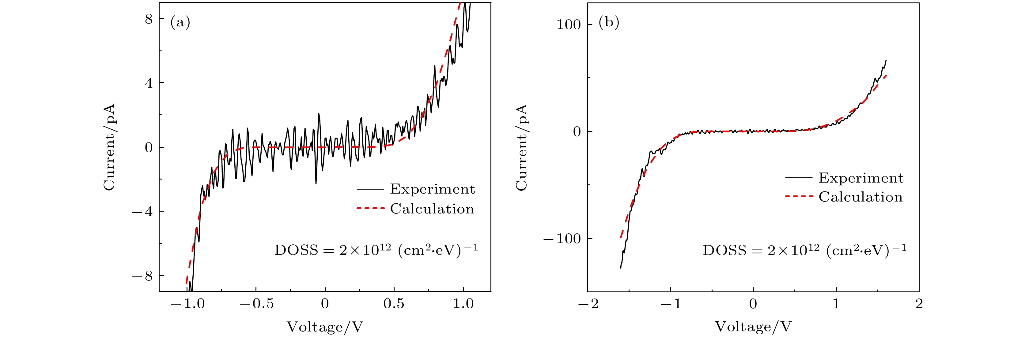
图 5 (a) InGaAs的I-V谱的计算(红色虚线)结果与实验谱线(黑色实线)的对比; (b) 图(a)谱线在整个(–1.6 V, 1.6 V)电压范围对计算/实验对比结果的呈现
Fig. 5. (a) Comparison of the I-V spectra between the calculated (red dashed line) and experimental (black solid line); (b) comparison of the spectra within the whole voltage range of (–1.6 V, 1.6 V).
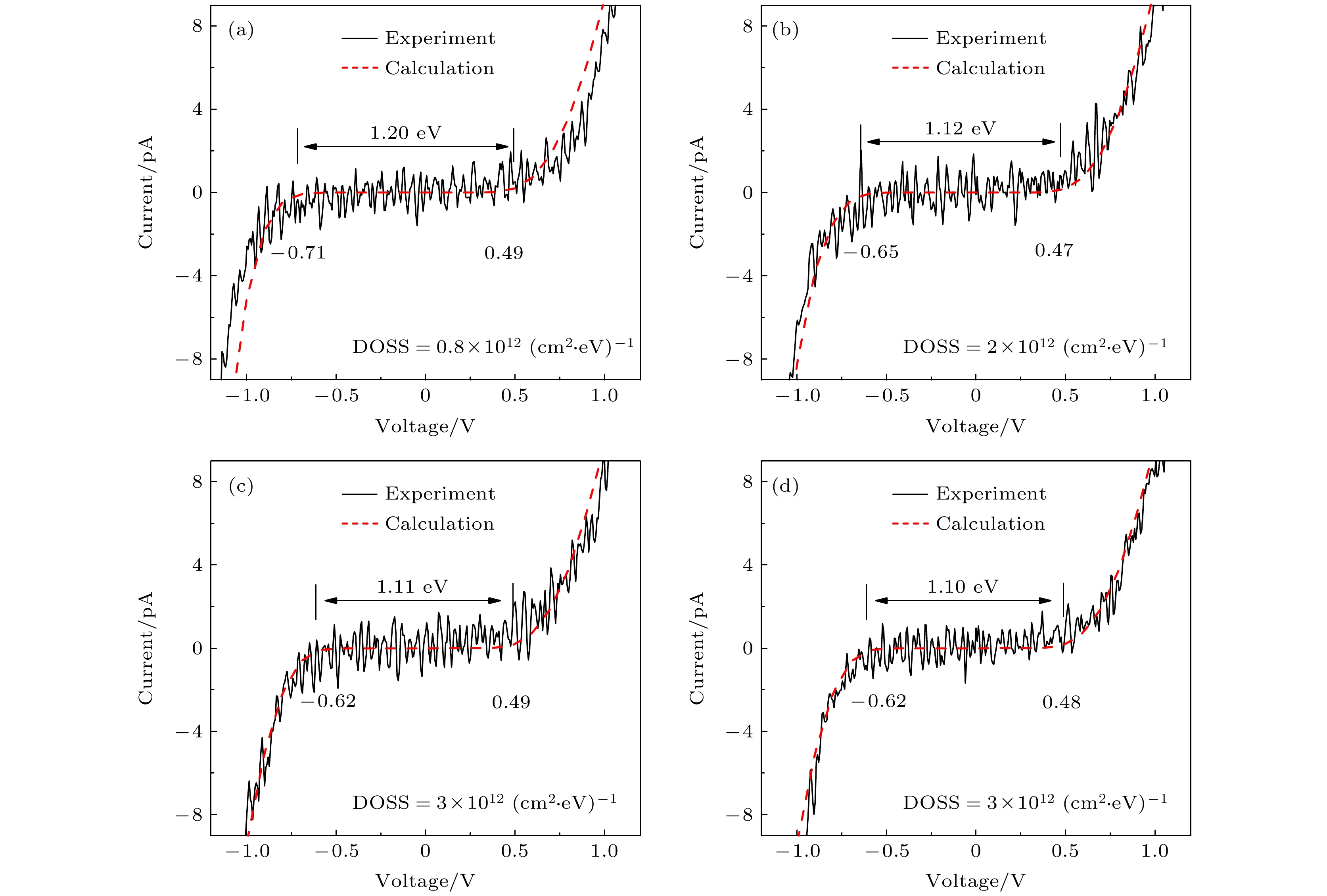
图 6 (a)—(d) InGaAs的四组I-V谱实验谱线(黑色实线)与模型计算(红色虚线)的比对, 各图中分别注明了计算时采用的表面态密度(DOSS)数值
Fig. 6. (a)–(d) Comparison of four groups of experimental I-V spectra (black solid lines) with the corresponding calculated I-V spectra (red dashed line). The DOSS for each curve is indicated, respectively.
表 1 InGaAs隧道谱特征参量的实验数据与TIBB模型计算的对比
Table 1. Comparison of experimental data and TIBB model calculations on the characteristic parameters of InGaAs tunneling spectra.
The parameters of
I-V spectraApparent band gap/eV V–onset/V V+onset/V Experimental 1.13 –0.67 0.46 Calculations
with the
density of surface
states/(cm2·eV)–10 1.25 –0.89 0.36 1.0 × 10¹¹ 1.29 –0.89 0.40 1.0 × 10¹² 1.21 –0.75 0.46 2.0 × 10¹² 1.11 –0.66 0.45 1.0 × 10¹³ 0.90 –0.49 0.41  下载: 导出CSV
-
[1] Tian Z, Gan Y, Zhang T, Wang B, Ji H, Feng Y, Xue J 2019 Phys. Rev. B 100 085440
Google Scholar
[2] Lee D H, Gupta J A 2010 Science 330 1807
Google Scholar
[3] Wijnheijmer A P, Garleff J K, Teichmann K, Wenderoth M, Loth S, Ulbrich R G, Maksym P A, Roy M, Koenraad P M 2009 Phys. Rev. Lett. 102 166101
Google Scholar
[4] Timm R, Feenstra R M, Eisele H, Lenz A, Ivanova L, Lenz E, and Dähne M 2009 J. Appl. Phys 105 093718
Google Scholar
[5] Huang B C, Chiu Y P, Huang P C, Wang W C, Tra V T, Yang J C, He Q, Lin J Y, Chang C S, Chu Y H 2012 Phys. Rev. lett. 109 246807
Google Scholar
[6] Lin H, Lagoute J, Repain V, Chacon C, Girard Y, Lauret J -S, Ducastelle F, Loiseau A, Rousset S 2010 Nat. Mater. 9 235
Google Scholar
[7] Shao F, Zha F X, Pan B C, Shao J, Zhao X L, Shen X C 2014 Phys. Rev. B 89 085423
Google Scholar
[8] Feenstra R M 2003 J. Vac. Sci. Technol. B 21 2080
Google Scholar
[9] Feenstra R M 2009 Surf. Sci. 603 2841
Google Scholar
[10] Feenstra R M, Gaan S, Meyer G, Rieder K H 2005 Phys. Rev. B 71 125316
Google Scholar
[11] Dong Y, Feenstra R M, Semtsiv M P, Masselink W T 2008 J. Appl. Phys. 103 073704
Google Scholar
[12] Ishida N, Sueoka K, Feenstra R M 2009 Phys. Rev. B 80 075320
Google Scholar
[13] Rouvié A, Coussement J, Huet O, Truffer JP, Pozzi M, Oubensaid E H, Hamard S, Maillart P, Costard E 2014 Proc. of SPIE 9249 92490Z
Google Scholar
[14] Wen J, Wang W J, Chen X R, Li N, Chen X S, Lu W 2018 J. Appl. Phys. 123 161530
Google Scholar
[15] 郑文龙, 张亚光, 顾溢, 李宝宝, 陈泽中, 陈平平 2019 红外与毫米波学报 38 1001
Zheng W L, Zhang Y G, Gu Y, Li B B, Chen Z Z, Chen P P 2019 J. Infrared Millim. Waves 38 1001
[16] Zha F X, Hong F, Pan B C, Wang Y, Shao J, Shen X C 2018 Phys. Rev. B 97 035401
Google Scholar
[17] Mikkelsen A, Lundgren E 2005 Prog. Surf. Sci. 80 1
Google Scholar
[18] Feenstra R M 1994 Phys. Rev. B 50 4561
Google Scholar
[19] Albrektsen O, Arent D J, Meier H P, Salemink H W M, 1990 Appl. Phys. Lett. 57 31
Google Scholar
[20] Newman N, Spicer W E, Kendelewicz T, Lindau I 1986 J. Vac. Sci. Technol. B 4 931
Google Scholar
[21] 邓宗武, 郭伟民, 刘焕明, 曹立礼 1999 物理化学学报 15 303
Google Scholar
Deng Z W, Kwok Raymund W M, Lau Leo W M, Cao L L 1999 Acta Phys-Chim. Sin. 15 303
Google Scholar
[22] Kingston R H, Neustadter S F 1955 J. Appl. Phys 26 718
Google Scholar
[23] Seiwatz R, Green M 1958 J. Appl. Phys 29 1034
Google Scholar
[24] Jäger N D, Weber E R, Urban K, Ebert P H 2003 Phys. Rev. B 67 165327
Google Scholar
[25] Ivanova L, Borisova S, Eisele H, Dähne M, Laubsch A, Ebert P H 2008 Appl. Phys. Lett. 93 192110
Google Scholar

 下载:
下载:
计量
- 文章访问数: 9689
- PDF下载量: 212
- 被引次数: 0
