


-
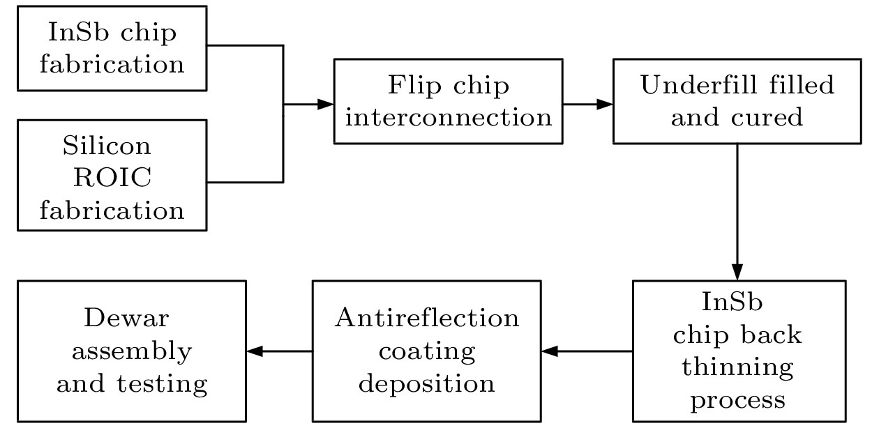
批量生产中经常发生的锑化铟(InSb)芯片碎裂问题制约着InSb红外焦平面探测器(IRFPAs)成品率的提升. 经分析认为: 低周期液氮冲击下发生在器件边沿区域的InSb芯片破碎与该区域中迸溅金点的存在有关. 为从理论上明晰迸溅金点对InSb芯片局部碎裂的影响, 本文建立了包含迸溅金点的InSb IRFPAs结构模型, 分析了迸溅金点的存在对应力分布的影响. 在此基础上, 在应力集中处预置不同长度的初始裂纹用以描述InSb晶片中的位错, 以能量释放率为判据, 探究InSb芯片碎裂与迸溅金点和位错线长短的关系. 结论如下: 1) 迸溅金点的存在对InSb芯片碎裂的影响是局部的, 在迸溅金点与InSb芯片接触区域的两侧会形成两个应力集中点; 2) 环绕预置裂纹的能量释放率会随着预置裂纹长度的增加而加速增大, 当预置裂纹长度接近InSb芯片上表面时, 能量释放率近乎指数增加, 并在预置裂纹贯穿InSb芯片时达到最大值; 3) 迸溅金点引起的InSb芯片破碎属于I型断裂失效模式, 在多周期液氮冲击中, 位错线在应力集中效应的驱使下逐步扩展, 直至贯穿InSb芯片, 最终形成宏观碎裂失效现象.
-
关键词:
- 锑化铟红外焦平面探测器 /
- 迸溅金点 /
- 热应力分布 /
- 能量释放率
Local cleavage of indium antimonide (InSb) chip always occurs in the manufacture of the InSb infrared focal plane detectors (IRFPAs), and this specific fracture phenomenon restricts the improvement of the yield of the InSb IRFPAs. After analysis, we think that the cleavage of InSb chip in the edge region of the InSb IRFPAs is related to the splashed gold bump existing in this region, and this failure phenomenon dominates in the low-cyclic liquid nitrogen shocking tests. In order to clarify the influence of the splashed gold bump on the cleavage of the InSb chip, we establish a structural model of the InSb IRFPAs containing the splashed gold bump, and analyze the influence of the splashed gold bump on the thermal stress distribution in the InSb chip. Besides, we preset the initial cracks with different lengths at the stress concentration sites to describe the dislocations in InSb wafers. Using the energy release rate as criterion, we obtain the relationship between the cleavage of the InSb chip and the dislocation line length in the presence of splashed gold bump. The main conclusions are drawn as follows. 1) The influence of the splashed gold bump on the cleavage of the InSb chip is localized, and two stress concentration sites are formed in the outermost part of the contact region between the splashed gold bump and the InSb chip. 2) The energy release rate surrounding the preset crack increases promptly with the preset crack length increasing. 3) Cleavage of the InSb chip caused by the splashed gold bump belongs to the type I fracture failure mode. In the cyclic liquid nitrogen shocking tests, the dislocation line gradually punches through the InSb chip under the driving of the concentrating stress, and forms the macro cleavage of the InSb chip.-
Keywords:
- InSb infrared focal plane detectors /
- splashed gold bump /
- thermal stress distribution /
- energy release rate
[1] 吕衍秋, 鲁星, 鲁正雄, 李墨 2020 航空兵器 27 1
 Google Scholar
Lv Y Q, Lu X, Lu Z X, Li M 2020 Aero Weaponry 27 1
Google Scholar
[2] Rogalski A 2011 Infrared Phys. Technol. 54 136
Google Scholar
[3] 胡伟达, 李庆, 陈效双, 陆卫 2019 物理学报 68 120701
Google Scholar
Hu W D, Li Q, Chen X S, Lu W 2019 Acta Phys. Sin. 68 120701
Google Scholar
[4] Bhan R K, Dhar V 2019 Opto-Electron. Rev. 27 174
Google Scholar
[5] 罗宏 2010 激光与红外 40 720
Google Scholar
Luo H 2010 Laser & Infrared 40 720
Google Scholar
[6] Meng Q D, Zhang X L, Lv Y Q, Si J J 2019 Opt. Quantum Electron. 51 1
Google Scholar
[7] Meng Q D, Zhang X L, Lv Y Q, Si J J 2017 Opt. Quantum Electron. 49 211
Google Scholar
[8] Hao L C, Huang A B, Lai C X, Chen X, Hao M M, Chen H L, Lu G G, Huang Y, En Y F 2015 Aopc: Optical & Optoelectronic Sensing & Imaging Technology Beijing, China, May 5−7, 2015 96740H-1
[9] 秦朗 2014 硕士学位论文 (辽宁: 大连理工大学)
Qin L 2014 M. S. Thesis (Liaoning: Dalian University of Technology) (in Chinese)
[10] 巩锋, 程鹏, 吴卿, 折伟林, 陈元瑞 2013 激光与红外 43 1146
Google Scholar
Gong F, Cheng P, Wu Q, She W L, Chen Y R 2013 Laser & Infrared 43 1146
Google Scholar
[11] 柏伟, 庞新义, 赵超 2018 红外 39 8
Google Scholar
Bai W, Pang X Y, Zhao C 2018 Infrared 39 8
Google Scholar
[12] Rybicki E F, Kanninen M F 1977 Eng. Fract. Mech. 9 931
Google Scholar
[13] Irwin G R 1956 Sagamore Res. Conf. Proc. 2 289
[14] Zhang X L, Meng Q D, Lv Y Q, Si J J 2017 Infrared Phys. Technol. 86 207
Google Scholar
[15] Zhang L W, Meng Q D, Zhang X L, Yu Q, Lv Y Q, Si J J 2013 Infrared Phys. Technol. 60 29
Google Scholar
[16] Zhang L W, Meng Q D, Zhang X L, Lv Y Q 2014 J. Mech. Sci. Technol. 28 2281
Google Scholar
[17] Liu X H, Suo Z, Ma Q, Fujimoto H 2000 Eng. Fract. Mech. 66 387
Google Scholar
-

图 2 线性虚拟裂纹闭合技术原理
Fig. 2. Principle of virtual crack closure technique for linear crack.

图 4 迸溅金点存在与否情况下InSb芯片下表面的面内正应力分布
Fig. 4. Distributions of the in-plane normal stress in bottom surface of InSb chip with splashed gold bump or not.

图 5 不同裂纹扩展长度下InSb芯片中能量释放率的演化过程
Fig. 5. Evolution process of energy release rate in InSb chip under different crack propagation lengths.
表 1 InSb IRFPAs模型的相关材料参数
Table 1. Material parameters of InSb IRFPAs model.
Materials Elastic modulus
E/GPaPoison’s
ratio μTemperatures
T/KInSb chip 409 (in plane) 0.3500 77–300 123 (out of plane) Underfill 0.0002/α 0.3000 77–300 silicon ROIC 163 0.2800 77–300 Indium bump 20.54 0.4326 76 16.24 0.4408 187 12.70 0.4498 370 Negative electrode 79 0.4400 77–300 注: $ \alpha = 22.46 \times {10^{ - 6}} + 5.04 \times {10^{ - 8}} \times {\text{(}}T-273{\text{)}} $, 其中 T 是Kelvin温度.  下载: 导出CSV
-
[1] 吕衍秋, 鲁星, 鲁正雄, 李墨 2020 航空兵器 27 1
Google Scholar
Lv Y Q, Lu X, Lu Z X, Li M 2020 Aero Weaponry 27 1
Google Scholar
[2] Rogalski A 2011 Infrared Phys. Technol. 54 136
Google Scholar
[3] 胡伟达, 李庆, 陈效双, 陆卫 2019 物理学报 68 120701
Google Scholar
Hu W D, Li Q, Chen X S, Lu W 2019 Acta Phys. Sin. 68 120701
Google Scholar
[4] Bhan R K, Dhar V 2019 Opto-Electron. Rev. 27 174
Google Scholar
[5] 罗宏 2010 激光与红外 40 720
Google Scholar
Luo H 2010 Laser & Infrared 40 720
Google Scholar
[6] Meng Q D, Zhang X L, Lv Y Q, Si J J 2019 Opt. Quantum Electron. 51 1
Google Scholar
[7] Meng Q D, Zhang X L, Lv Y Q, Si J J 2017 Opt. Quantum Electron. 49 211
Google Scholar
[8] Hao L C, Huang A B, Lai C X, Chen X, Hao M M, Chen H L, Lu G G, Huang Y, En Y F 2015 Aopc: Optical & Optoelectronic Sensing & Imaging Technology Beijing, China, May 5−7, 2015 96740H-1
[9] 秦朗 2014 硕士学位论文 (辽宁: 大连理工大学)
Qin L 2014 M. S. Thesis (Liaoning: Dalian University of Technology) (in Chinese)
[10] 巩锋, 程鹏, 吴卿, 折伟林, 陈元瑞 2013 激光与红外 43 1146
Google Scholar
Gong F, Cheng P, Wu Q, She W L, Chen Y R 2013 Laser & Infrared 43 1146
Google Scholar
[11] 柏伟, 庞新义, 赵超 2018 红外 39 8
Google Scholar
Bai W, Pang X Y, Zhao C 2018 Infrared 39 8
Google Scholar
[12] Rybicki E F, Kanninen M F 1977 Eng. Fract. Mech. 9 931
Google Scholar
[13] Irwin G R 1956 Sagamore Res. Conf. Proc. 2 289
[14] Zhang X L, Meng Q D, Lv Y Q, Si J J 2017 Infrared Phys. Technol. 86 207
Google Scholar
[15] Zhang L W, Meng Q D, Zhang X L, Yu Q, Lv Y Q, Si J J 2013 Infrared Phys. Technol. 60 29
Google Scholar
[16] Zhang L W, Meng Q D, Zhang X L, Lv Y Q 2014 J. Mech. Sci. Technol. 28 2281
Google Scholar
[17] Liu X H, Suo Z, Ma Q, Fujimoto H 2000 Eng. Fract. Mech. 66 387
Google Scholar

 下载:
下载:

计量
- 文章访问数: 6099
- PDF下载量: 57
- 被引次数: 0
