


-
本文利用基于密度泛函理论(DFT)的第一性原理计算研究了SrVO3/SrTiO3(111)超晶格的电子结构、电学和磁学性质. 研究结果表明, SrVO3/SrTiO3(111)超晶格可通过调节间隔层SrTiO3的厚度实现铁磁半金属-铁磁绝缘体的转变. SrVO3亚层之间可以通过厚度为2个原子层的SrTiO3间隔层发生层间耦合, 超晶格呈现铁磁半金属态; 当间隔层SrTiO3的厚度等于3个原子层时, 超晶格出现小的带隙(约0.28 eV); 当间隔层SrTiO3的厚度大于3个原子层时, 超晶格出现较大带隙, 呈现铁磁绝缘态. 进一步对SrVO3/SrTiO3界面附近由于Ti-V混合导致的缺陷界面进行研究发现, 界面附近的Ti-V混合对金属-绝缘体转变具有重要的影响: 与理想界面相比, Ti-V混合的缺陷界面更能抑制层间耦合, 诱导超晶格实现铁磁半金属-铁磁绝缘体的转变. 本研究结果为SrVO3/SrTiO3(111)超晶格通过调控间隔层SrTiO3层数实现铁磁半金属-铁磁绝缘体的转变提供了理论依据.In this work, the first-principle calculations based on density functional theory (DFT) are employed to investigate the electronic and magnetic properties of SrVO3/SrTiO3(111) superlattices. The studies show that the transition from ferromagnetic half-metal to ferromagnetic insulator can be achieved by adjusting the thickness of the spacer-layer SrTiO3. The interlayer coupling between the SrVO3 sublayers can occur across two unit-cell (uc) distance of SrTiO3, and the superlattice is ferromagnetic half-metal. When the SrTiO3 sublayers are 3uc, a small band gap (about 0.28 eV) appears in the superlattice. When the SrTiO3 sublayers are more than 3uc, the superlattice has a large band gap and exhibits ferromagnetic insulating state. Further studies show that the Ti-V mixed defects play an important role in realizing the transition of metal-insulator. Compared with the ideal interface, the Ti-V mixed interface can inhibit the interlayer coupling and induce the transition of ferromagnetic half-metal to ferromagnetic insulator. These results provide a theoretical basis for the transition of ferromagnetic half-metal to ferromagnetic insulator by adjusting the number of SrTiO3 layers in SrVO3/SrTiO3(111) superlattices.
-
Keywords:
- superlattice /
- metal-insulator transition /
- ferromagnetic half-metal /
- ferromagnetic insulator
[1] Moyer J A, Eaton C, Engel-Herbert R 2013 Adv. Mater. 25 3578
 Google Scholar
[2] Zhang L, Zhou Y, Guo L, Zhao W, Barnes A, Zhang H-T, Eaton C, Zheng Y, Brahlek M, Haneef H F, Podraza N J, Chan M H W, Gopalan V, Rabe K M, Engel-Herbert R 2016 Nat. Mater. 15 204
Google Scholar
[3] Kim D H, Kim D W, Kang B S, Noh T W, Lee D R, Lee K B, Lee S J 2000 Solid State Commun. 114 473
Google Scholar
[4] Wang J, Gauquelin N, Huijben M, Verbeeck J, Rijnders G, Koster G 2020 Appl. Phys. Lett. 117 133105
Google Scholar
[5] Wang G, Wang Z, Meng M, Saghayezhian M, Chen L, Chen C, Guo H, Zhu Y, Plummer W, Zhang J 2019 Phys. Rev. B 100 155114
Google Scholar
[6] Pardo V, Pickett W E 2010 Phys. Rev. B 81 245117
Google Scholar
[7] Sohn C, Skoropata E, Choi Y, Gao X, Rastogi A, Huon A, McGuire M A, Nuckols L, Zhang Y, Freeland J W, Haskel D, Lee H N 2019 Adv. Mater. 31 1805389
Google Scholar
[8] Meng D, Guo H, Cui Z, Ma C, Zhao J, Lu J, Xu H, Wang Z, Hu X, Fu Z, Peng R, Guo J, Zhai X, Brown G J, Knize R, Lu Y 2018 PNAS 115 2873
Google Scholar
[9] Okamoto S, Zhu W, Nomura Y, Arita R, Xiao D, Nagaosa N 2014 Phys. Rev. B 89 195121
Google Scholar
[10] Beltrán J I, Muñoz M C 2017 Phys. Rev. B 95 245120
Google Scholar
[11] Verissimo-Alves M, Garcia-Fernandez P, Bilc D L, Ghosez P, Junquera J 2012 Phys. Rev. Lett. 108 107003
Google Scholar
[12] Cossu F, Jilili J, Schwingenschlögl U 2014 Adv. Mater. Interfaces 1 1400057
Google Scholar
[13] Song G, Zhang W 2014 Sci. Rep. UK 4 4564
Google Scholar
[14] Cossu F, Kim H S, Sanyal B, Di Marco I 2022 NPJ Comp. Mater. 8 1
Google Scholar
[15] Yao X, Yi H T, Jain D, Han M G, Oh S 2021 Nano Lett. 21 5914
Google Scholar
[16] Cen C, Thiel S, Hammerl G, Schneider C W, Andersen K E, Hellberg C S, Mannhart J, Levy J 2008 Nat. Mater. 7 298
Google Scholar
[17] 李云, 鲁文建 2021 物理学报 70 218503
Google Scholar
Li Y, Lu W J 2021 Acta Phys. Sin. 70 218503
Google Scholar
[18] Li J, Yin D, Li Q, Sun R, Huang S, Meng F 2017 Phys. Chem. Chem. Phys. 19 6945
Google Scholar
[19] Kalabukhov A S, Boikov Y A, Serenkov I T, Sakharov V I, Popok V N, Gunnarsson R, Borjesson J, Ljustina N, Olsson E, Winkler D, Claeson T 2009 Phys. Rev. Lett. 103 146101
Google Scholar
[20] Kramer B, MacKinnon A, 1993 Rep. Prog. Phys. 56 1469
Google Scholar
[21] Kresse G, Furthmüller J 1996 Phys. Rev. B 54 11169
Google Scholar
[22] Blöchl P E 1994 Phys. Rev. B 50 17953
Google Scholar
[23] Perdew J P, Burke K, Ernzerhof M 1996 Phys. Rev. Lett. 77 3865
Google Scholar
[24] Anisimov V I, Zaanen J, Andersen O K 1991 Phys. Rev. B 44 943
Google Scholar
[25] Du Y L, Wang C L, Li J C, Xu P P, Zhang X H, Liu J, Su W B, Mei L M 2014 Chin. Phys. B 23 087302
Google Scholar
[26] Park S Y, Kumar A, Rabe K M 2017 Phys. Rev. Lett. 118 087602
Google Scholar
[27] Monkhorst H J, Pack J D 1976 Phys. Rev. B 13 5188
Google Scholar
[28] Kuganathan N, Baiutti F, Morata A, Tarancon A, Chroneos A 2021 AIP Adv. 11 075029
Google Scholar
[29] Musa Saad HE M 2021 B. Mater. Sci. 44 1
Google Scholar
[30] Du Y L, Bu H X, Ji C J, Zhang X M, Li C L, Fang X N 2019 Phys. Chem. Chem. Phys. 21 18170
Google Scholar
[31] Xiong L, Yi L, Gao G Y 2014 J. Magn. Magn. Mater. 349 69
Google Scholar
[32] 贾倩, 杜颖妍, 杜成旭, 陈婷, 刘焦, 于越, 张恒源, 刘明, 毋志民 2019 功能材料 50 12183
Google Scholar
Jia Q, Du Y Y, Du C X, Chen T, Liu J, Yu Y, Zhang H Y, Liu M, Wu Z M 2019 J. Funct. Mater. 50 12183
Google Scholar
[33] Ohtomo A, Muller D A, Grazul J L, Hwang H Y 2002 Nature 419 378
Google Scholar
[34] Biscaras J, Bergeal N, Kushwaha A, Wolf T, Rastogi A, Budhani R C, Lesueur J 2010 Nat. Commun. 1 1
Google Scholar
[35] Xu Q F, Wu D, Li A D 2013 Phys. Lett. A 377 577
Google Scholar
[36] 范潆方 2019 硕士学位论文 (南京: 南京邮电大学)
Fan Y F 2019 M. S. Thesis (Nanjing: Nanjing University of Posts and Telecommunications) (in Chinese)
[37] Liu Z T Y, Podraza N J, Khare S V, Sarin P 2018 Comput. Mater. Sci. 144 139
Google Scholar
-
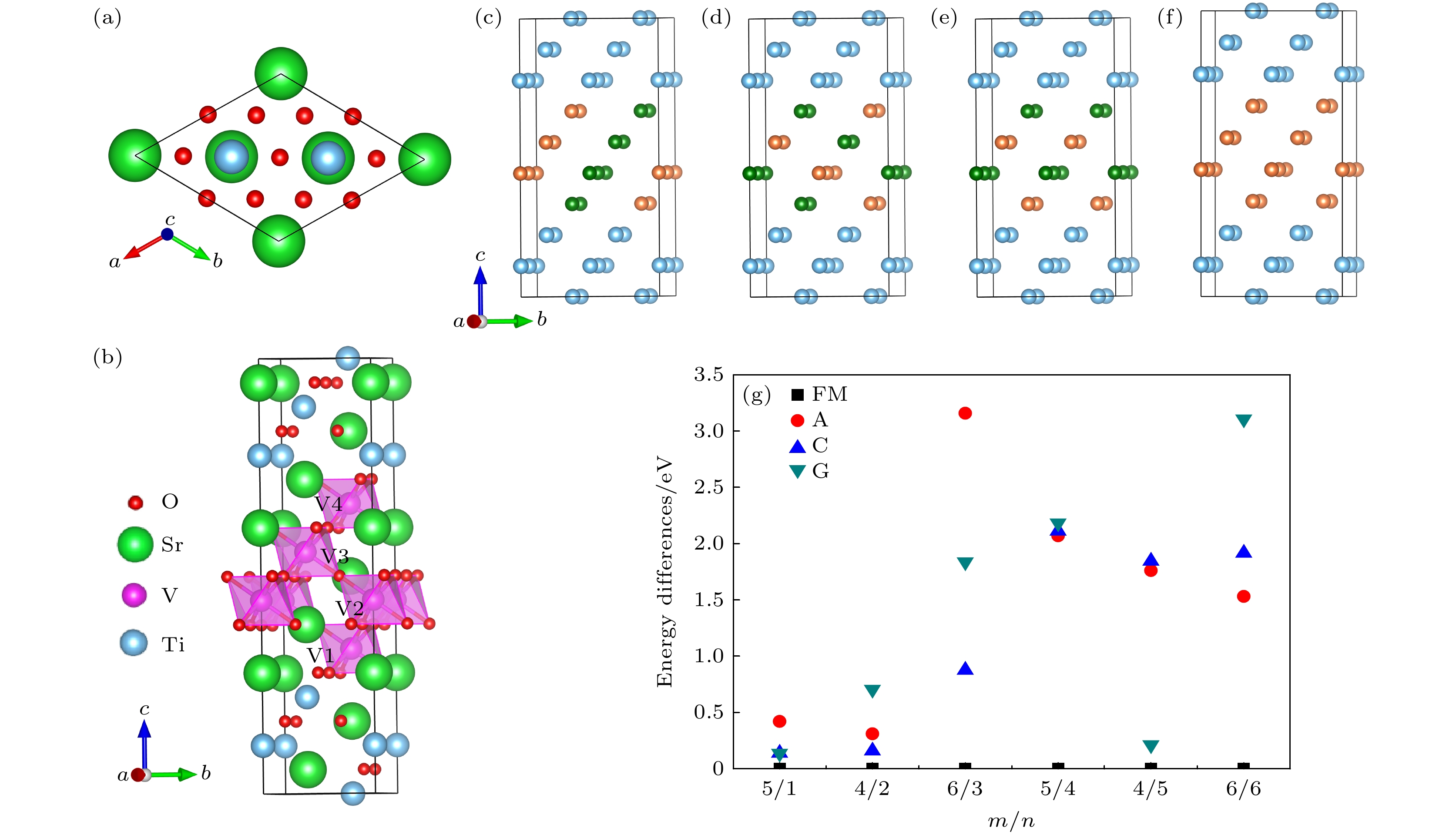
图 1 (a) 超晶格(SVO)m/(STO)n(111) (4 ≤ m ≤ 6; 1 ≤ n ≤ 6)的模型之一(SVO)4/(STO)5 (111) 超晶格的顶视图; (b) 超晶格(SVO)4/(STO)5(111) 的侧视图; (c) A-AFM示意图; (d) C-AFM示意图; (e) G-AFM示意图; (f) FM示意图; (g) 各模型基态能量的对比图, 其中铁磁态能量设为零; 图(c)—(f)中, 只显示了Ti和V原子, 其中蓝色小球代表Ti原子, 紫色小球代表自旋向上的V原子, 绿色小球代表自旋向下的V原子
Fig. 1. (a) Top view of the (SVO)4/(STO)5(111) superlattice, which is one of the (SVO)m/(STO)n (111) (
4 ≤ m ≤ 6; 1 ≤ n ≤ 6) superlattices; (b) side view of (SVO)4/(STO)5(111) superlattice; (c) schematic diagram of A-AFM; (d) schematic diagram of C-AFM; (e) schematic diagram of G-AFM; (f) schematic diagram of FM; (g) energy differences between different magnetic orders of different superlattices. In the figure, the energy of FM states are set to zero. In figures (c)–(f) , only the Ti and V atoms are shown, the blue balls represent the Ti atoms, the purple balls represent the spin-up V atoms, and the green balls represent the spin-down V atoms. 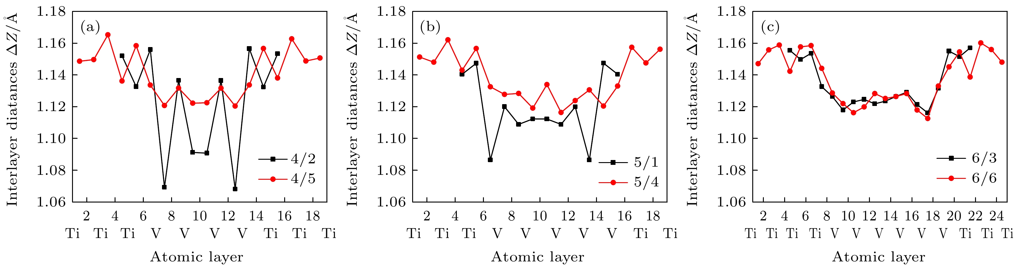
图 2 沿c轴方向, 各超晶格相邻原子层间距离对比图 (a) (SVO)4/(STO)2 和(SVO)4/(STO)5; (b) (SVO)5/(STO)1和 (SVO)5/(STO)4; (c) (SVO)6/(STO)3和 (SVO)6/(STO)6
Fig. 2. The interplanar distance between consecutive planes of different superlattices along the c axis: (a) (SVO)4/(STO)2 and (SVO)4/(STO)5; (b) (SVO)5/(STO)1 and (SVO)5/(STO)4; (c) (SVO)6/(STO)3 and (SVO)6/(STO)6.

图 3 超晶格在费米能级附近的能带结构和总态密度的对比图 (a) (SVO)5/(STO)1 (111); (b) (SVO)4/(STO)2 (111); (c) (SVO)6/(STO)3 (111); (d) (SVO)5/(STO)4 (111); (e) (SVO)4/(STO)5 (111); (f) (SVO)6/(STO)6 (111). 高对称点如图中第一布里渊区所示; 对应的总态密度图显示在能带图下侧, 黑色实线和红色实线分别代表自旋向上和自旋向下, 费米能级用虚线表示
Fig. 3. Comparison of band structures and total state densities near the Fermi level of different superlattices: (a) (SVO)5/(STO)1 (111); (b) (SVO)4/(STO)2 (111); (c) (SVO)6/(STO)3 (111); (d) (SVO)5/(STO)4 (111); (e) (SVO)4/(STO)5 (111); (f) (SVO)6/(STO)6 (111). The inset shows the Brillouin zone and the special points. Black and red lines are spin-up and spin-down states,respectively; the Fermi level is located at 0 eV (dotted black line).
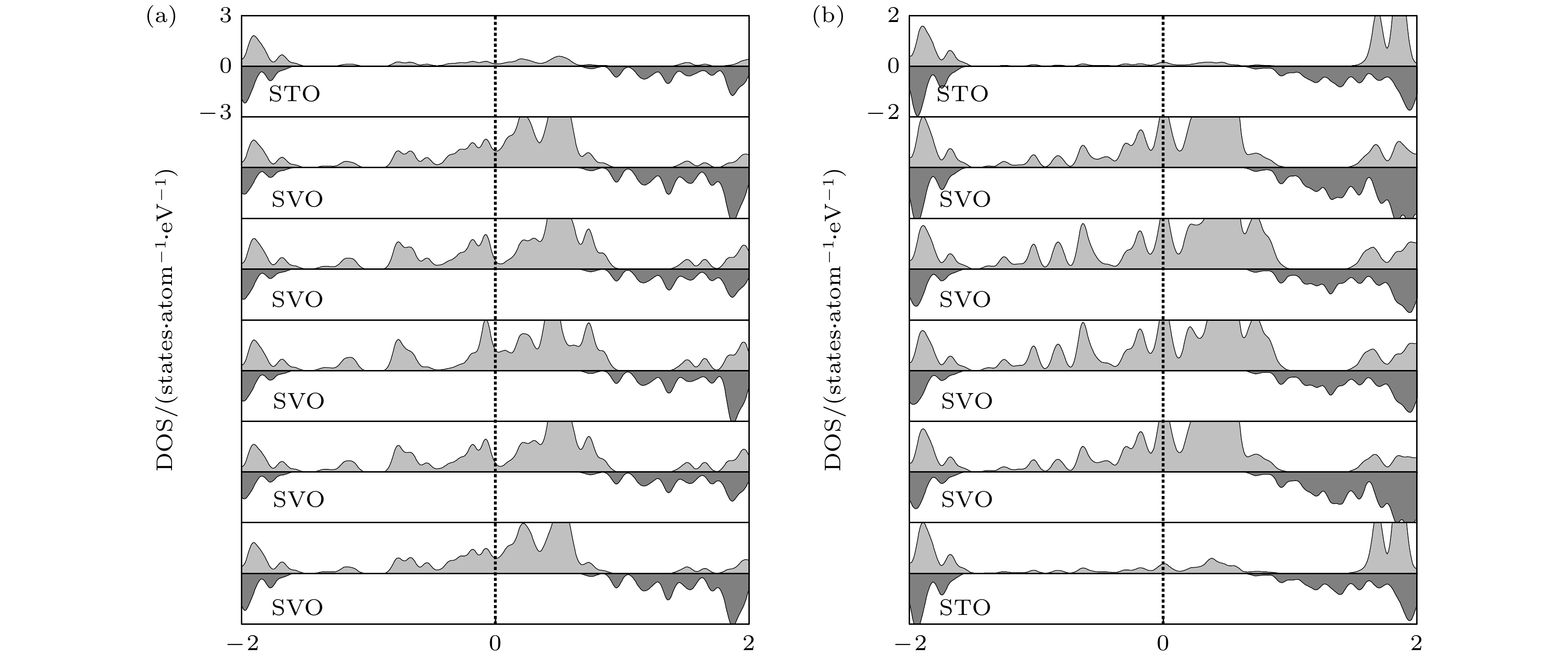
图 4 (a), (b) (SVO)5/(STO)1 (111)和(SVO)4/(STO)2 (111)超晶格各原子层在费米能级附近的态密度图. 图中自旋向上的电子态密度由浅灰色区域表示, 自旋向下的电子态密度由深灰色区域表示; 黑色虚线表示费米能级
Fig. 4. (a), (b) Layer-resolved partial DOS of (SVO)5/(STO)1(111) and (SVO)4/(STO)2 (111) superlattices. Light gray and dark gray areas are spin-up and spin-down states, respectively. The Fermi level is located at 0 eV (dotted black line).
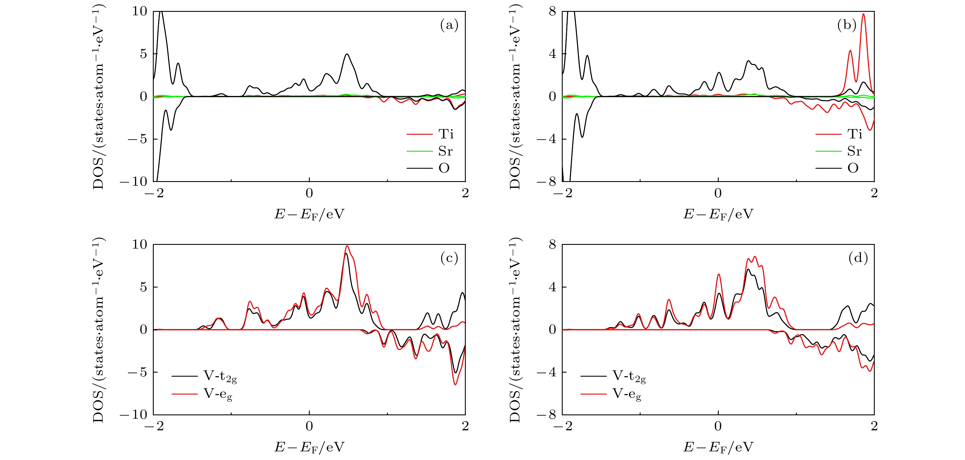
图 5 (SVO)5/(STO)1 (111) (a)和 (SVO)4/(STO)2 (111) (b)超晶格中 Ti, Sr, O 原子的态密度图; (SVO)5/(STO)1 (111) (c)和 (SVO)4/(STO)2 (111) (d)超晶格中V 原子 3d 轨道的分波态密度图, 黑色虚线表示费米能级
Fig. 5. Densities of states near the Fermi level of Ti, Sr and O in (SVO)5/(STO)1 (111) (a) and (SVO)4/(STO)2 (111) (b) superlattices; the partial density of states of V 3d orbitals of (SVO)5/(STO)1 (111) (c) and (SVO)4/(STO)2 (111) (d) superlattices. The Fermi level is located at 0 eV (dotted black line).

图 6 各超晶格V 原子 3d 轨道的分波态密度图 (a) (SVO)5/(STO)1 (111); (b) (SVO)4/(STO)2 (111); (c) (SVO)6/(STO)3 (111); (d) (SVO)5/(STO)4 (111); (e) (SVO)4/(STO)5 (111); (f) (SVO)6/(STO)6 (111). 其中, 图(b)中V原子的位置与图1(b)中V原子位置一致, 其余模型中V原子的排列与图1(b)中V原子排列相似, 从下往上V原子序号递增. 图中黑色虚线表示费米能级
Fig. 6. The partial density of states of V 3d orbitals of different superlattices: (a) (SVO)5/(STO)1 (111); (b) (SVO)4/(STO)2 (111); (c) (SVO)6/(STO)3 (111); (d) (SVO)5/(STO)4 (111); (e) (SVO)4/(STO)5 (111); (f) (SVO)6/(STO)6 (111). Among them, the position of the V atoms in figure (b) are consistent with the position of the V atoms in Fig. 1(b). The arrangement of V atoms in the rest of the models is similar to the arrangement of V atoms in Fig. 1(b). The atomic numbers get bigger and bigger from the bottom up. The Fermi level is located at 0 eV (dotted black line).
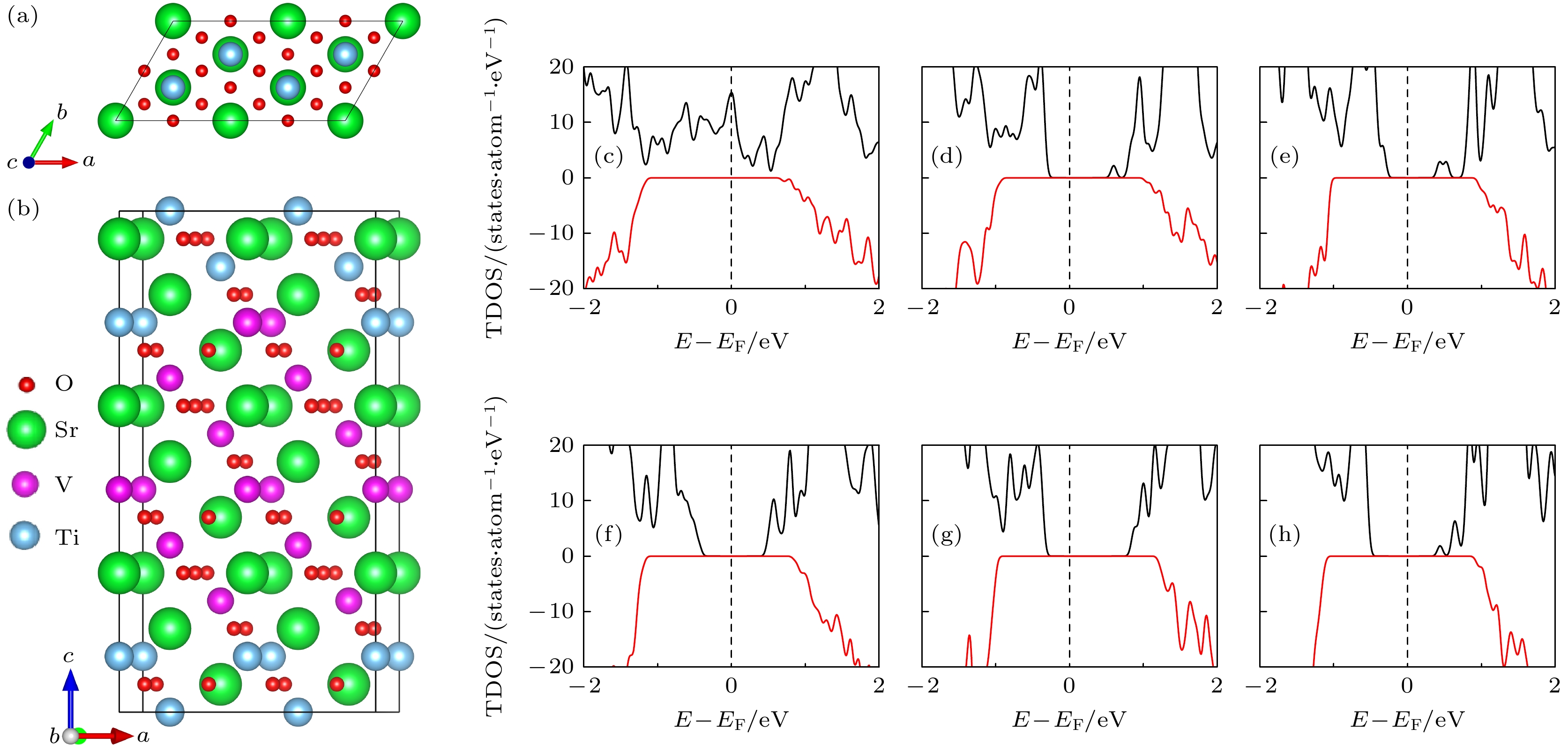
图 7 (a) 含有Ti-V混合缺陷界面的(SVO)m/(ST0.5V0.5O)1/(STO)n-1(111) (4 ≤ m ≤ 6; 1 ≤ n ≤ 6)超晶格之一 (SVO)5/(ST0.5V0.5O)1/(STO)3(111) 的俯视图; (b) (SVO)5/(ST0.5V0.5O)1/(STO)3(111) 超晶格的侧视图; (c)—(h) 各含有Ti-V混合缺陷界面的超晶格在费米能级附近的总态密度的对比图, 其中, (c) (SVO)5/(ST0.5V0.5O)1(111); (d) (SVO)4/(ST0.5V0.5O)1/(STO)1(111); (e) (SVO)6/(ST0.5V0.5O)1/(STO)2(111); (f) (SVO)5/(ST0.5V0.5O)1/(STO)3(111); (g) (SVO)4/(ST0.5V0.5O)1/(STO)4(111); (h) (SVO)6/(ST0.5V0.5O)1/(STO)5(111). 黑色实线和红色实线分别代表自旋向上和自旋向下, 费米能级用虚线表示
Fig. 7. (a) Top view of (SVO)5/(ST0.5V0.5O)1/(STO)3(111) superlattice containing the defect interface; (b) side view of (SVO)5/(ST0.5V0.5O)1/(STO)3(111) superlattice; (c)–(h) comparison of total state densities near the Fermi level for the different superlattices, (c) (SVO)5/(ST0.5V0.5O)1(111); (d) (SVO)4/(ST0.5V0.5O)1/(STO)1(111); (e) (SVO)6/(ST0.5V0.5O)1/(STO)2(111); (f) (SVO)5/(ST0.5V0.5O)1/(STO)3(111); (g) (SVO)4/(ST0.5V0.5O)1/(STO)4(111); (h) (SVO)6/(ST0.5V0.5O)1/(STO)5(111). Black and red lines are spin-up and spin-down states, respectively. The Fermi level is located at 0 eV (dotted black line).
表 1 不同(SVO)m/(STO)n(111)超晶格模型的面内晶格常数
Table 1. In-plane lattice constants of the different (SVO)m/(STO)n(111) superlattices.
m/n 4/2 4/5 5/1 5/4 6/3 6/6 面内晶格常数/Å 5.50 5.57 5.48 5.57 5.56 5.57  下载: 导出CSV
表 2 (SVO)m/(STO)n (111)各超晶格V和O的磁矩及体系总磁矩, 各模型中 V 原子的排列与图 1(b)中 V 原子排列相似, 从下往上V 原子的序号递增
Table 2. Magnetic moments of V and O atoms and the total magnetic moments of (SVO)m/(STO)n (111) superlattices. The arrangement of V atoms in the models is similar to the arrangement of V atoms in Fig. 1(b). The atomic numbers get bigger and bigger from the bottom up.
m/n 5/1 4/2 6/3 5/4 4/5 6/6 M_v1/μB 1.13 1.01 1.00 1.00 1.00 1.01 M_v2/μB 1.18 1.20 1.02 1.02 1.01 1.00 M_v3/μB 1.04 1.20 1.00 1.02 1.01 1.02 M_v4/μB 1.04 1.01 1.02 1.00 1.00 1.01 M_v5/μB 1.18 1.00 1.00 1.01 M_v6/μB 1.00 1.01 M_Vtotal/μB 5.57 4.42 6.04 5.04 4.02 6.06 M_O/μB –0.93 –0.74 –0.32 –0.28 –0.23 –0.34 M_Total/μB 5.0 4.0 6.0 5.0 4.0 6.0
下载: 导出CSV
表 3 (SVO)m/(STO)n(111)各理想界面与Ti-V混合缺陷界面超晶格自旋向上态密度带隙值
Table 3. Band gaps of spin-up states of (SVO)m/(STO)n(111) superlattices with ideal or defect interfaces.
Band gap of spin-up states/eV m/n 5/1 4/2 6/3 5/4 4/5 6/6 Ideal interfaces 0 0 0.28 0.51 1.00 0.48 Defect interfaces 0 0.69 0.56 0.74 1.03 0.77
下载: 导出CSV
-
[1] Moyer J A, Eaton C, Engel-Herbert R 2013 Adv. Mater. 25 3578
Google Scholar
[2] Zhang L, Zhou Y, Guo L, Zhao W, Barnes A, Zhang H-T, Eaton C, Zheng Y, Brahlek M, Haneef H F, Podraza N J, Chan M H W, Gopalan V, Rabe K M, Engel-Herbert R 2016 Nat. Mater. 15 204
Google Scholar
[3] Kim D H, Kim D W, Kang B S, Noh T W, Lee D R, Lee K B, Lee S J 2000 Solid State Commun. 114 473
Google Scholar
[4] Wang J, Gauquelin N, Huijben M, Verbeeck J, Rijnders G, Koster G 2020 Appl. Phys. Lett. 117 133105
Google Scholar
[5] Wang G, Wang Z, Meng M, Saghayezhian M, Chen L, Chen C, Guo H, Zhu Y, Plummer W, Zhang J 2019 Phys. Rev. B 100 155114
Google Scholar
[6] Pardo V, Pickett W E 2010 Phys. Rev. B 81 245117
Google Scholar
[7] Sohn C, Skoropata E, Choi Y, Gao X, Rastogi A, Huon A, McGuire M A, Nuckols L, Zhang Y, Freeland J W, Haskel D, Lee H N 2019 Adv. Mater. 31 1805389
Google Scholar
[8] Meng D, Guo H, Cui Z, Ma C, Zhao J, Lu J, Xu H, Wang Z, Hu X, Fu Z, Peng R, Guo J, Zhai X, Brown G J, Knize R, Lu Y 2018 PNAS 115 2873
Google Scholar
[9] Okamoto S, Zhu W, Nomura Y, Arita R, Xiao D, Nagaosa N 2014 Phys. Rev. B 89 195121
Google Scholar
[10] Beltrán J I, Muñoz M C 2017 Phys. Rev. B 95 245120
Google Scholar
[11] Verissimo-Alves M, Garcia-Fernandez P, Bilc D L, Ghosez P, Junquera J 2012 Phys. Rev. Lett. 108 107003
Google Scholar
[12] Cossu F, Jilili J, Schwingenschlögl U 2014 Adv. Mater. Interfaces 1 1400057
Google Scholar
[13] Song G, Zhang W 2014 Sci. Rep. UK 4 4564
Google Scholar
[14] Cossu F, Kim H S, Sanyal B, Di Marco I 2022 NPJ Comp. Mater. 8 1
Google Scholar
[15] Yao X, Yi H T, Jain D, Han M G, Oh S 2021 Nano Lett. 21 5914
Google Scholar
[16] Cen C, Thiel S, Hammerl G, Schneider C W, Andersen K E, Hellberg C S, Mannhart J, Levy J 2008 Nat. Mater. 7 298
Google Scholar
[17] 李云, 鲁文建 2021 物理学报 70 218503
Google Scholar
Li Y, Lu W J 2021 Acta Phys. Sin. 70 218503
Google Scholar
[18] Li J, Yin D, Li Q, Sun R, Huang S, Meng F 2017 Phys. Chem. Chem. Phys. 19 6945
Google Scholar
[19] Kalabukhov A S, Boikov Y A, Serenkov I T, Sakharov V I, Popok V N, Gunnarsson R, Borjesson J, Ljustina N, Olsson E, Winkler D, Claeson T 2009 Phys. Rev. Lett. 103 146101
Google Scholar
[20] Kramer B, MacKinnon A, 1993 Rep. Prog. Phys. 56 1469
Google Scholar
[21] Kresse G, Furthmüller J 1996 Phys. Rev. B 54 11169
Google Scholar
[22] Blöchl P E 1994 Phys. Rev. B 50 17953
Google Scholar
[23] Perdew J P, Burke K, Ernzerhof M 1996 Phys. Rev. Lett. 77 3865
Google Scholar
[24] Anisimov V I, Zaanen J, Andersen O K 1991 Phys. Rev. B 44 943
Google Scholar
[25] Du Y L, Wang C L, Li J C, Xu P P, Zhang X H, Liu J, Su W B, Mei L M 2014 Chin. Phys. B 23 087302
Google Scholar
[26] Park S Y, Kumar A, Rabe K M 2017 Phys. Rev. Lett. 118 087602
Google Scholar
[27] Monkhorst H J, Pack J D 1976 Phys. Rev. B 13 5188
Google Scholar
[28] Kuganathan N, Baiutti F, Morata A, Tarancon A, Chroneos A 2021 AIP Adv. 11 075029
Google Scholar
[29] Musa Saad HE M 2021 B. Mater. Sci. 44 1
Google Scholar
[30] Du Y L, Bu H X, Ji C J, Zhang X M, Li C L, Fang X N 2019 Phys. Chem. Chem. Phys. 21 18170
Google Scholar
[31] Xiong L, Yi L, Gao G Y 2014 J. Magn. Magn. Mater. 349 69
Google Scholar
[32] 贾倩, 杜颖妍, 杜成旭, 陈婷, 刘焦, 于越, 张恒源, 刘明, 毋志民 2019 功能材料 50 12183
Google Scholar
Jia Q, Du Y Y, Du C X, Chen T, Liu J, Yu Y, Zhang H Y, Liu M, Wu Z M 2019 J. Funct. Mater. 50 12183
Google Scholar
[33] Ohtomo A, Muller D A, Grazul J L, Hwang H Y 2002 Nature 419 378
Google Scholar
[34] Biscaras J, Bergeal N, Kushwaha A, Wolf T, Rastogi A, Budhani R C, Lesueur J 2010 Nat. Commun. 1 1
Google Scholar
[35] Xu Q F, Wu D, Li A D 2013 Phys. Lett. A 377 577
Google Scholar
[36] 范潆方 2019 硕士学位论文 (南京: 南京邮电大学)
Fan Y F 2019 M. S. Thesis (Nanjing: Nanjing University of Posts and Telecommunications) (in Chinese)
[37] Liu Z T Y, Podraza N J, Khare S V, Sarin P 2018 Comput. Mater. Sci. 144 139
Google Scholar

 下载:
下载:
计量
- 文章访问数: 6551
- PDF下载量: 99
- 被引次数: 0
