-
能谷光子晶体是研究拓扑光子学的重要平台之一, 基于能谷光子晶体的新型光波导支持抗散射传输的能谷依赖边界态, 提高了波导中的急弯传输效率, 为光信息高效传输提供了新思路. 另一方面, 对称性在拓扑学和光子晶体研究中具有重要的物理意义和研究价值. 例如, 能谷光子晶体在破缺空间反演对称性的情况下表现出类量子能谷霍尔效应. 目前, 大多数能谷光子晶体具有C3对称性, 而具有更低对称性的能谷光子晶体是否能够支持拓扑光传输仍然需要研究. 本文通过调整能谷光子晶体的原胞形貌, 构建了低对称性能谷光子晶体, 并研究了其边界态的传输特性. 研究结果表明, 相对于C3对称性能谷光子晶体, 低对称性能谷光子晶体的光子禁带变窄, 但其边界态仍然能够实现单向激发以及抗散射传输. 这一发现丰富了拓扑光子结构的多样性, 为在低对称性结构中寻找拓扑保护光传输行为提供了指导.Valley photonic crystals represent a cornerstone in the field of topological photonics, which promotes the development of cutting-edge photonic waveguides. These waveguides support robust transmission by using valley-dependent edge states. This innovation marks a great leap forward in enhancing transmission efficiency, (especially in sharp bends), thus opening up a new way for efficient optical information transmission. However, although the role of symmetry in topology and photonic crystals cannot be exaggerated, it is worth noting that valley photonic crystals provide a unique platform for exploring the interplay between symmetry and topological phenomena. An intriguing analogy between valley photonic crystals and the quantum valley Hall effect is an example, which will be shown when the symmetry of spatial inversion is broken. At present, the characteristic of most valley photonic crystals is C3-rotational symmetry, which leads to an interesting study, that is, whether crystals with lower symmetry can also support topological light transmission. In order to solve this problem head-on, our work focuses on constructing and characterizing valley photonic crystals with low symmetry by carefully adjusting the unit cell morphology. Through theoretical analysis and numerical simulation, we unveil the remarkable ability of these low-symmetry valley photonic crystals to facilitate topological light transport. Initially, we analyze the bulk bands of these low-symmetry crystals, observing a narrowed photonic band gap and a shift in the irreducible Brillouin zone compared with C3-rotation symmetric crystals. To examine edge state transmission, we calculate dispersion relations and electric field distributions, revealing two edge states with opposite phase chirality at the same frequency. Using this point, we achieve unidirectional excitation of edge states. Additionally, we manipulate the refractive index of the surrounding medium and explore various scenarios of external light beam coupling. Moreover, we investigate the robust transmission of edge states, demonstrating smooth passage of light through sharp corners in Z-shaped bend waveguides without backscattering. In conclusion, our findings underscore the pivotal role played by edge states in facilitating unidirectional excitation and robust transmission in low-symmetry valley photonic crystals. By enriching the diversity of topological photonic structures and providing valuable insights into the behavior of topological light transport in structures with lower symmetry, our work contributes to the ongoing quest for novel photonic platforms with enhanced functions and performance.
-
Keywords:
- valley photonic crystal /
- symmetry /
- topological light transport
[1] Khanikaev A B, Shvets G 2017 Nat. Photonics 11 763
 Google Scholar
[2] Ozawa T, Price H M, Amo A, Goldman N, Hafezi M, Lu L, Rechtsman M C, Schuster D, Simon J, Zilberberg O, Carusotto I 2019 Rev. Mod. Phys. 91 015006
 Google Scholar
[3] Kim M, Jacob Z, Rho J 2020 Light-Sci. Appl. 9 130
 Google Scholar
[4] Bisharat D J, Davis R J, Zhou Y, Bandaru P R, Sievenpiper D F 2021 IEEE Antennas Propag. Mag. 63 112
 Google Scholar
[5] Xiao M, Zhang Z Q, Chan C T 2014 Phys. Rev. X 4 021017
[6] St-Jean P, Goblot V, Galopin E, Lemaître A, Ozawa T, Le Gratiet L, Sagnes I, Bloch J, Amo A 2017 Nat. Photonics 11 651
 Google Scholar
[7] Yang Y H, Gao Z, Xue H R, Zhang L, He M J, Yang Z J, Singh R J, Chong Y D, Zhang B L, Chen H S 2019 Nature 565 622
 Google Scholar
[8] Haldane F D M, Raghu S 2008 Phys. Rev. Lett. 100 013904
 Google Scholar
[9] Wang Z, Chong Y D, Joannopoulos J D, Soljacic M 2009 Nature 461 772
 Google Scholar
[10] Fang K J, Yu Z F, Fan S H 2012 Nat. Photonics 6 782
 Google Scholar
[11] Khanikaev A B, Mousavi S H, Tse W K, Kargarian M, MacDonald A H, Shvets G 2013 Nat. Mater. 12 233
 Google Scholar
[12] Lai K, Ma T, Bo X, Anlage S, Shvets G 2016 Sci. Rep. 6 28453
 Google Scholar
[13] Cheng X J, Jouvaud C, Ni X, Hossein Mousavi S, Genack A Z, Khanikaev A B 2016 Nat. Mater. 15 542
 Google Scholar
[14] Jalali Mehrabad M, Foster A P, Dost R, Clarke E, Patil P K, Farrer I, Heffernan J, Skolnick M S, Wilson L R 2020 Appl. Phys. Lett. 116 061102
 Google Scholar
[15] Liu J W, Shi F L, He X T, Tang G J, Chen W J, Chen X D, Dong J W 2021 Adv. Phys. X 6 1905546
[16] Xue H R, Yang Y H, Zhang B L 2021 Adv. Photon. Res. 2 2100013
 Google Scholar
[17] Ma T, Shvets G 2016 New J. Phys. 18 025012
 Google Scholar
[18] Chen X D, Zhao F L, Chen M, Dong J W 2017 Phys. Rev. B 96 020202
 Google Scholar
[19] Ye L P, Yang Y P, Hang Z H, Qiu C Y, Liu Z Y 2017 Appl. Phys. Lett. 111 251107
 Google Scholar
[20] Gao Z, Yang Z J, Gao F, Xue H R, Yang Y H, Dong J W, Zhang B L 2017 Phys. Rev. B 96 201402
 Google Scholar
[21] Wu X X, Meng Y, Tian J X, Huang Y Z, Xiang H, Han D Z, Wen W J 2017 Nat. Commun. 8 1304
 Google Scholar
[22] Noh J, Huang S, Chen K P, Rechtsman M C 2018 Phys. Rev. Lett. 120 063902
 Google Scholar
[23] Dubrovkin A M, Chattopadhyay U, Qiang B, Buchnev O, Wang Q J, Chong Y D, Zheludev N I 2020 Appl. Phys. Lett. 116 191105
 Google Scholar
[24] Chen Q L, Zhang L, He M J, Wang Z J, Lin X, Gao F, Yang Y H, Zhang B L, Chen H S 2019 Adv. Opt. Mater. 7 1900036
 Google Scholar
[25] Wong S, Saba M, Hess O, Oh S S 2020 Phys. Rev. Res. 2 012011
 Google Scholar
[26] Gao F, Xue H R, Yang Z J, Lai K, Yu Y, Lin X, Chong Y D, Shvets G, Zhang B L 2018 Nat. Phys. 14 140
[27] He X T, Liang E T, Yuan J J, Qiu H Y, Chen X D, Zhao F L, Dong J W 2019 Nat. Commun. 10 872
 Google Scholar
[28] Shalaev M I, Walasik W, Tsukernik A, Xu Y, Litchinitser N M 2019 Nat. Nanotechnol. 14 31
 Google Scholar
[29] Zeng Y Q, Chattopadhyay U, Zhu B F, Qiang B, Li J H, Jin Y H, Li L H, Davies A G, Linfield E H, Zhang B L, Chong Y D, Wang Q J 2020 Nature 578 246
 Google Scholar
[30] Barik S, Karasahin A, Mittal S, Waks E, Hafezi M 2020 Phys. Rev. B 101 205303
 Google Scholar
-
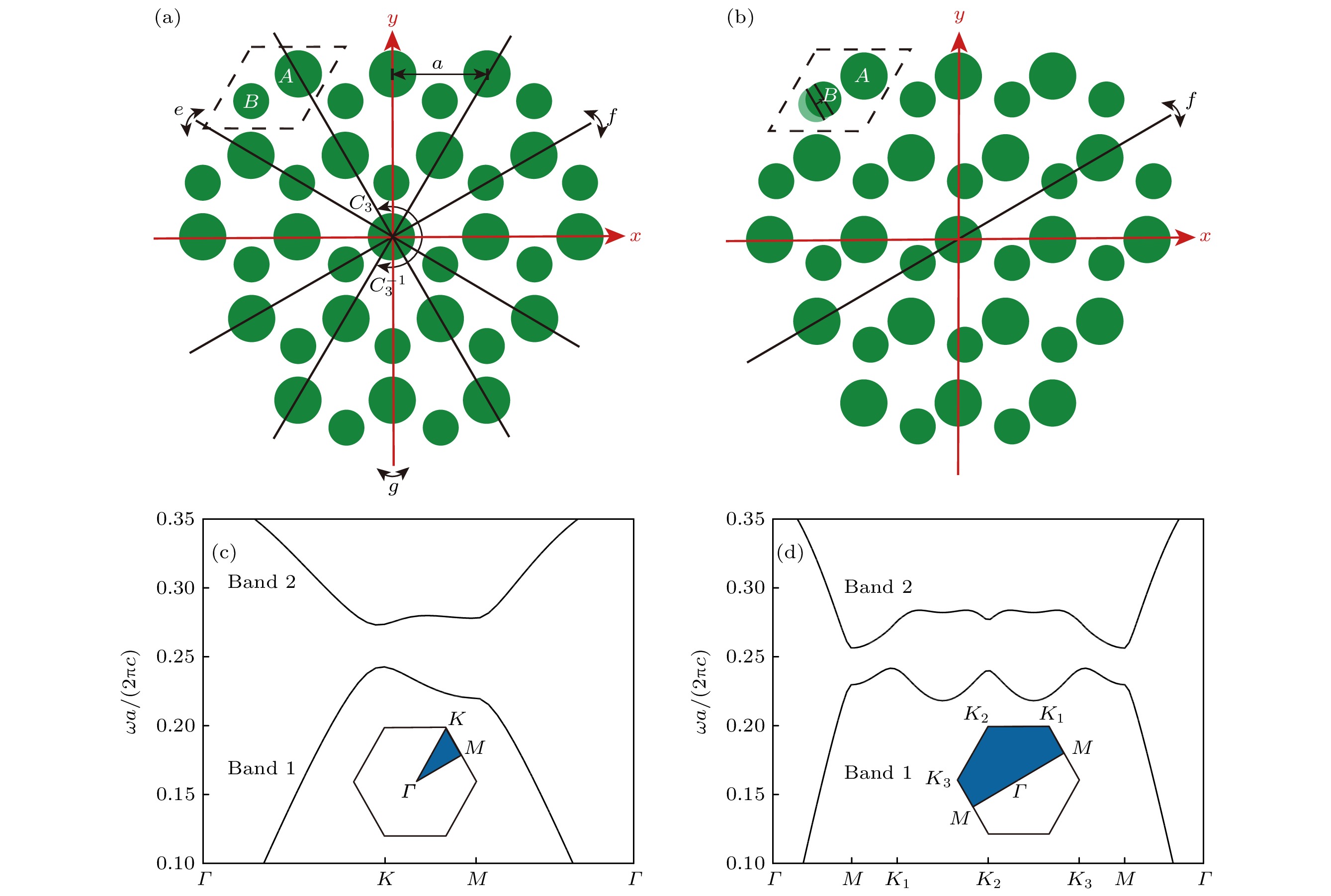
图 1 能谷光子晶体结构及能带 (a) C3对称性能谷光子晶体结构示意图, 该结构由具有相同晶格常数的三角格子交错构成, 一个原胞包含A, B两个硅柱子(虚线菱形), 空白部分为空气. A柱子直径为0.5a, B柱子直径为0.38a, 所有柱子的相对介电常数为11.7, 相对磁导率为1. 图中标注了该结构具有的对称轴和对称操作, 均用黑色实线和箭头表示. (b)低对称性能谷光子晶体结构示意图, 在C3对称性光子晶体原胞的基础上将柱子B沿着菱形对角线方向向柱子A平移0.08a, 其他条件均保持不变. (c) C3对称性能谷光子晶体体能带, 图中画出了横磁模式的两条频率最低的体能带, 并标注了第一布里渊区以及简约布里渊区(Γ-K-M构成的三角形区域, 蓝色填充区域). (d) 低对称性能谷光子晶体体能带, Γ-M-K1-K2-K3-M构成简约布里渊区(蓝色填充区域)
Fig. 1. Schematic structure and bulk band of valley photonic crystals: (a) Schematic of C3 symmetry valley photonic crystal and its symmetry analysis, the structure is composed of two interlaced triangular lattices with the same lattice constant, a unit cell contains two silicon rods A and B (dashed rhombus), and the background is air. The diameter of A rod is 0.5a and the diameter of B rod is 0.38a where a is the lattice constant, the dielectric constant of all rods is 11.7 and the permeability is 1. The symmetries are labelled in the figure and are represented by black solid lines and arrows. (b) Schematic of low-symmetry valley photonic crystal and symmetry analysis, we translate rod B along the diagonal of the rhombus towards rod A with a distance of 0.08a. (c) Bulk band of C3-symmetry valley photonic crystal, two lowest bulk bands of TM mode are shown. The first and irreducible Brillouin zones (the triangle region composed of Γ-K-M) are also labelled. (d) Bulk band of low symmetry valley photonic crystal, and the region composed of Γ-M-K1-K2-K3-M is the irreducible Brillouin zone (blue filled area).
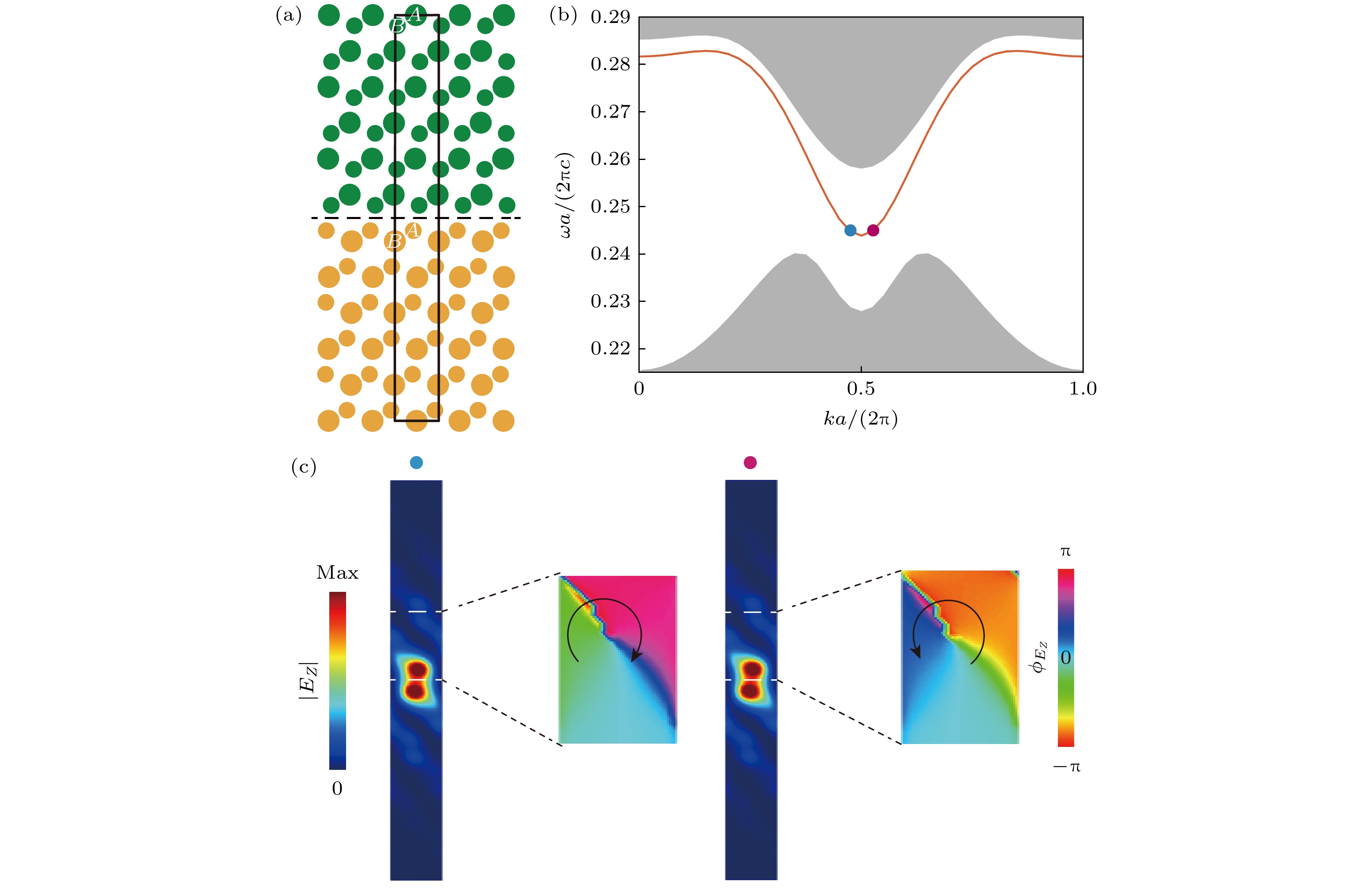
图 2 低对称性能谷光子晶体的边界态 (a)边界示意图, 由直径为0.5a的A柱与直径为0.38a的B柱构成的能谷光子晶体(绿色)和直径为0.38a的A柱与直径为0.5a的B柱构成的能谷光子晶体(黄色)拼接构建了边界; (b) 边界态色散曲线, 其中灰色填充区域对应体态, 橙色曲线对应边界态, 两个圆点标记0.245c/a频率下的两个边界态; (c) 两个边界态的电场强度分布图和电场相位分布图, 黑色箭头表示相位递减方向
Fig. 2. Edge states of low-symmetry valley photonic crystal: (a) Schematic of boundary which is built between one valley photonic crystal (green) and the other valley photonic crystal (yellow); (b) the band dispersion of edge states, grey area represents bulk states and orange curve represents edge states, two edge states at 0.245c/a are represented by two dots; (c) electric field intensity distribution and phase distribution of two edge states at 0.245c/a, the black arrow indicates the direction of the phase vortex.
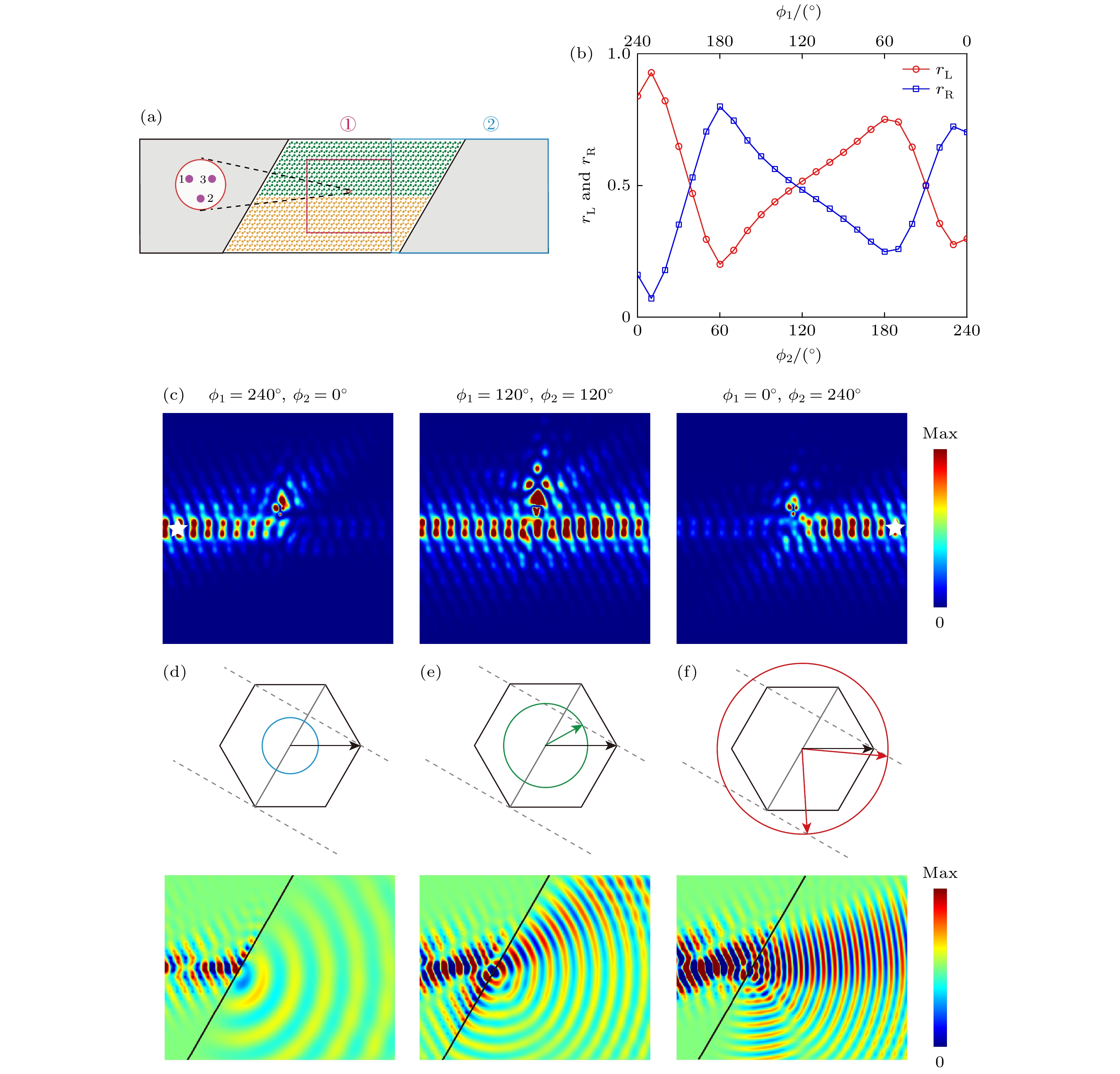
图 3 低对称性能谷光子晶体边界态的单向激发及外耦合 (a) 边界态单向激发示意图, 灰色区域为介质背景, 3个单极子置于波导中间作为激发源, 工作频率为0.245c/a, 红色方框表示单向激发的研究区域(用①标注), 蓝色方框表示外耦合的研究区域(用②标注); (b) 改变单极子1和2的相位, 保持单极子3相位不变, 得到激发源左右两侧的电场比值; (c) 单极子相位变化时激发源左右两侧的电场强度分布图; (d)—(f) 3种边界态外耦合情况, 第1行为波矢空间分析图, 灰色实线表示边界, 灰色虚线表示垂直于边界的方向, 箭头表示波矢方向. 第2行为对应的场分布图, 黑色实线表示边界
Fig. 3. Unidirectional excitation and external coupling of edge states of low-symmetry valley photonic crystal: (a) Schematic of unidirectional excitation of edge states. The gray area is the dielectric layer. Three input monopoles are placed in the middle as the excitation source and the working frequency is 0.245c/a, the red box represents the study area of unidirectional excitation (labeled with ①), the blue box represents the study area of external coupling (labeled with ②); (b) ratio of electric field at the left and right sides of the excitation source when the phase of monopole 3 is kept unchanged, but the phases of monopoles 1 and 2 are changed; (c) electric field intensity distribution for different input sources; (d)–(f) three cases of external coupling of edge state, wave vector space analysis is placed in the first line, the gray solid line represents the boundary and the gray dashed line represents the direction which is perpendicular to the boundary, the arrow represents the direction of wave vector, corresponding field distribution is placed in the second line. The black solid line represents the boundary.
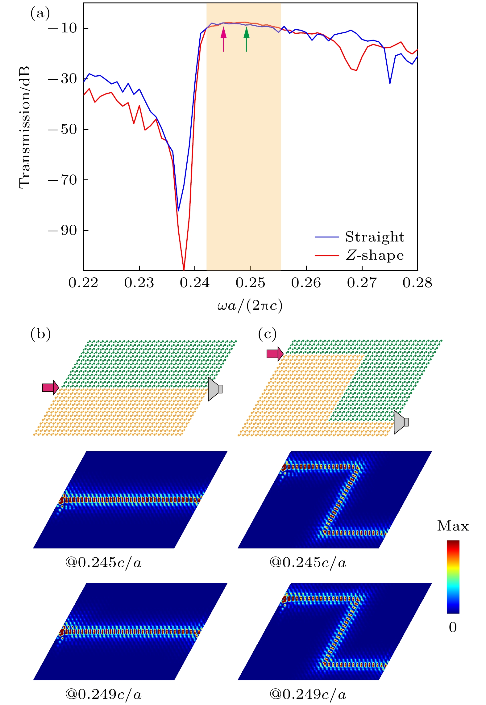
图 4 低对称性能谷光子晶体边界态的抗散射传输 (a) 直波导与Z形弯曲波导的透射谱(橙色区域表示体态禁带范围); (b)直波导结构示意图以及0.245c/a和0.249c/a频率下的电场强度分布图, 其中箭头表示发射端, 喇叭表示接受端; (c) Z形弯曲波导结构示意图以及0.245c/a和0.249c/a频率下的电场强度分布图
Fig. 4. Robust transmission of edge states of low-symmetry valley photonic crystal: (a) Transmission spectra for the Z-shaped bend waveguide and the straight waveguide (orange region represents the range of band gap); (b) schematic of straight waveguide and electric field intensity distribution of straight waveguide at 0.245c/a and 0.249c/a, the source is represented by arrow and the receiver is represented by horn; (c) schematic of Z-shaped bend waveguide and electric field intensity distribution of Z-shaped bend waveguide at 0.245c/a and 0.249c/a.
-
[1] Khanikaev A B, Shvets G 2017 Nat. Photonics 11 763
 Google Scholar
[2] Ozawa T, Price H M, Amo A, Goldman N, Hafezi M, Lu L, Rechtsman M C, Schuster D, Simon J, Zilberberg O, Carusotto I 2019 Rev. Mod. Phys. 91 015006
 Google Scholar
[3] Kim M, Jacob Z, Rho J 2020 Light-Sci. Appl. 9 130
 Google Scholar
[4] Bisharat D J, Davis R J, Zhou Y, Bandaru P R, Sievenpiper D F 2021 IEEE Antennas Propag. Mag. 63 112
 Google Scholar
[5] Xiao M, Zhang Z Q, Chan C T 2014 Phys. Rev. X 4 021017
[6] St-Jean P, Goblot V, Galopin E, Lemaître A, Ozawa T, Le Gratiet L, Sagnes I, Bloch J, Amo A 2017 Nat. Photonics 11 651
 Google Scholar
[7] Yang Y H, Gao Z, Xue H R, Zhang L, He M J, Yang Z J, Singh R J, Chong Y D, Zhang B L, Chen H S 2019 Nature 565 622
 Google Scholar
[8] Haldane F D M, Raghu S 2008 Phys. Rev. Lett. 100 013904
 Google Scholar
[9] Wang Z, Chong Y D, Joannopoulos J D, Soljacic M 2009 Nature 461 772
 Google Scholar
[10] Fang K J, Yu Z F, Fan S H 2012 Nat. Photonics 6 782
 Google Scholar
[11] Khanikaev A B, Mousavi S H, Tse W K, Kargarian M, MacDonald A H, Shvets G 2013 Nat. Mater. 12 233
 Google Scholar
[12] Lai K, Ma T, Bo X, Anlage S, Shvets G 2016 Sci. Rep. 6 28453
 Google Scholar
[13] Cheng X J, Jouvaud C, Ni X, Hossein Mousavi S, Genack A Z, Khanikaev A B 2016 Nat. Mater. 15 542
 Google Scholar
[14] Jalali Mehrabad M, Foster A P, Dost R, Clarke E, Patil P K, Farrer I, Heffernan J, Skolnick M S, Wilson L R 2020 Appl. Phys. Lett. 116 061102
 Google Scholar
[15] Liu J W, Shi F L, He X T, Tang G J, Chen W J, Chen X D, Dong J W 2021 Adv. Phys. X 6 1905546
[16] Xue H R, Yang Y H, Zhang B L 2021 Adv. Photon. Res. 2 2100013
 Google Scholar
[17] Ma T, Shvets G 2016 New J. Phys. 18 025012
 Google Scholar
[18] Chen X D, Zhao F L, Chen M, Dong J W 2017 Phys. Rev. B 96 020202
 Google Scholar
[19] Ye L P, Yang Y P, Hang Z H, Qiu C Y, Liu Z Y 2017 Appl. Phys. Lett. 111 251107
 Google Scholar
[20] Gao Z, Yang Z J, Gao F, Xue H R, Yang Y H, Dong J W, Zhang B L 2017 Phys. Rev. B 96 201402
 Google Scholar
[21] Wu X X, Meng Y, Tian J X, Huang Y Z, Xiang H, Han D Z, Wen W J 2017 Nat. Commun. 8 1304
 Google Scholar
[22] Noh J, Huang S, Chen K P, Rechtsman M C 2018 Phys. Rev. Lett. 120 063902
 Google Scholar
[23] Dubrovkin A M, Chattopadhyay U, Qiang B, Buchnev O, Wang Q J, Chong Y D, Zheludev N I 2020 Appl. Phys. Lett. 116 191105
 Google Scholar
[24] Chen Q L, Zhang L, He M J, Wang Z J, Lin X, Gao F, Yang Y H, Zhang B L, Chen H S 2019 Adv. Opt. Mater. 7 1900036
 Google Scholar
[25] Wong S, Saba M, Hess O, Oh S S 2020 Phys. Rev. Res. 2 012011
 Google Scholar
[26] Gao F, Xue H R, Yang Z J, Lai K, Yu Y, Lin X, Chong Y D, Shvets G, Zhang B L 2018 Nat. Phys. 14 140
[27] He X T, Liang E T, Yuan J J, Qiu H Y, Chen X D, Zhao F L, Dong J W 2019 Nat. Commun. 10 872
 Google Scholar
[28] Shalaev M I, Walasik W, Tsukernik A, Xu Y, Litchinitser N M 2019 Nat. Nanotechnol. 14 31
 Google Scholar
[29] Zeng Y Q, Chattopadhyay U, Zhu B F, Qiang B, Li J H, Jin Y H, Li L H, Davies A G, Linfield E H, Zhang B L, Chong Y D, Wang Q J 2020 Nature 578 246
 Google Scholar
[30] Barik S, Karasahin A, Mittal S, Waks E, Hafezi M 2020 Phys. Rev. B 101 205303
 Google Scholar
计量
- 文章访问数: 7553
- PDF下载量: 324
- 被引次数: 0


 下载:
下载:


