


-
In this paper, the resistive switching characteristics of Ag/BiFeO3/Fe2O3/ITO multilayer film deposited on ITO by magnetron sputtering are investigated. The Ag/BiFeO3/Fe2O3/ITO devices all exhibit superior resistive switching behaviors due to the formation of Ag conducting filaments. The resistive switching ratio of the device is close to 10 for the sample with 100 nm-thick Fe2O3 film. The current value of the device increases sharply at 0.56 V when the voltage is swept forward, and the device switches from LRS back to HRS at –0.3 V when a voltage of opposite polarity is applied. The I-V curves of the device are fitted in double logarithmic coordinates. It is found that the device is controlled by an Ohmic conduction model in the low resistance state and by two conduction models in the high resistance state: Ohmic conduction in the low bias region, and the SCLC conduction model at higher voltages. Such a resistive switching characteristic with very low switching voltage and a high resistance ratio is particularly important for the application of resistive stochastic storage. In addition, all samples show an obvious negative differential resistance effect, which is caused by Joule heating. The Ag/BiFeO3/Fe2O3/ITO device show both resistive switching characteristics and a negative differential resistance effect, which have important applications.
[1] Weitz R T, Walter A, Engl R, Sezi R, Dehm C 2006 Nano Lett. 6 2810
 Google Scholar
[2] Li X L, Jia J, Li Y C, Bai Y H, Li J, Shi Y N, Wang L F, Xu X H 2016 Sci. Rep. 6 31934
Google Scholar
[3] Bibes M, Barthélémy A 2008 Nat. Mater. 7 425
Google Scholar
[4] Miyake M, Scott J F, Lou X J, Morrison F D, Nonaka T, Motoyama S, Tatsuta T, Tsuji O 2008 J. Appl. Phys. 104 064112
Google Scholar
[5] Jensen W B 1997 J. Chem. Edu. 74 1063
Google Scholar
[6] Neale R G, Nelson D L, Moore G E 1970 Electronics 43 56
[7] Jeong D S, Thomas R, Katiyar R S, Scott J F, Kohlstedt H, Petraru A, Hwang C S 2012 Rep. Prog. Phys. 75 076502
Google Scholar
[8] Jeong D S, Choi B J, Hwang C S 2006 J. Appl. Phys. 100 113724
Google Scholar
[9] Yu S M, Guan X M, Wong H S P 2011 Appl. Phys. Lett. 99 063507
Google Scholar
[10] Hui F, Grustan-Gutierrez E, Long S B, Liu Q, Ott A K, Ferrari A C, Lanza M 2017 Adv. Electron. Mater. 3 1600195
Google Scholar
[11] Waser R 2012 J. Nanosci. Nanotechnol. 12 7628
Google Scholar
[12] Kim D C, Seo S, Ahn S E, Suh D S, Lee M J, Park B H, Yoo I K, Baek I G, Kim H J, Yim E K, Lee J E, Park S O, Kim H S, Chung U I, Moon J T, Ryu B I 2006 Appl. Phys. Lett. 88 202102
Google Scholar
[13] Mahapatra R, Maji S, Horsfall A B, Wright N G 2015 Microelectron. Eng. 138 118
Google Scholar
[14] Lee J S, Lee S, Noh T W 2015 App. Phys. Rev. 2 031303
Google Scholar
[15] Yoo H G, Kim S, Lee K J 2014 RSC Adv. 4 20017
Google Scholar
[16] Zhang W B, Wang C, Liu G, Wang J, Chen Y, Li R W 2014 Chem. Commun. 50 11496
Google Scholar
[17] He C T, Lu Y, Li X L, Chen P 2022 Acta Phys. Sin. 71 086102 [何朝滔, 卢羽, 李秀林, 陈鹏 2022 物理学报 71 086102]
Google Scholar
He C T, Lu Y, Li X L, Chen P 2022 Acta Phys. Sin. 71 086102
Google Scholar
[18] Zhang X W, He C T, Li X L, Qiu X Y, Zhang Y, Chen P 2022 Acta Phys. Sin. 71 187303 [张兴文, 何朝滔, 李秀林, 邱晓燕, 张耘, 陈鹏 2022 物理学报 71 187303]
Google Scholar
Zhang X W, He C T, Li X L, Qiu X Y, Zhang Y, Chen P 2022 Acta Phys. Sin. 71 187303
Google Scholar
[19] Guo T, Sun B, Zhou Y, Zhao H B, Lei M, Zhao Y 2018 PCCP 20 20635
Google Scholar
[20] Prakash C, Yadav A K, Dixit A 2023 Phys. Chem. Chem. Phys. 25 19868
Google Scholar
[21] Zhang K J, Ren K, Qin X Z, Zhu S H, Yang F, Zhao Y, Zhang Y 2021 IEEE Trans. Electron Dev. 68 3807
Google Scholar
[22] Kumar S, Strachan J P, Williams R S 2017 Nature 548 318
Google Scholar
[23] Kumar S, Williams R S, Wang Z 2020 Nature 585 518
Google Scholar
[24] Zhou G D, Gu D S, Ye J, Sun B, Shi H, Ran H, Ji'e M, Hu X, Wang L, Duan S, Ling H 2025 Adv. Mater. 37 e08107
Google Scholar
[25] Zhou G D, Duan S K, Li P, Sun B, Wu B, Yao Y Q, Yang X D, Han J J, Wu J G, Wang G, Liao L P, Lin C Y, Hu W, Xu C Y, Liu D B, Chen T, Chen L J, Zhou A K, Song Q L 2018 Adv. Electron. Mater. 4 1700567
Google Scholar
[26] Shuai Y, Zhou S Q, Bürger D, Helm M, Schmidt H 2011 J. Appl. Phys. 109 124117
Google Scholar
[27] Zheng P P, Sun B, Chen Y Z, Elshekh H, Yu T, Mao S S, Zhu S H, Wang H Y, Zhao Y, Yu Z 2019 Appl. Mater. Today 14 21
Google Scholar
[28] Lu Y, Tang Y Y, Li X L, He C T, Chen P 2022 App. Phys. A-Mater. 128 229
Google Scholar
[29] Tang M, Sun B, Huang J, Gao J, Li C M 2016 RSC Adv. 6 25028
Google Scholar
-

图 1 (a) Ag/BiFeO3/Fe2O3/ITO的结构图; (b) Fe2O3层厚度约为100 nm时器件的SEM截面
Fig. 1. (a) Schematic diagram of the Ag/BiFeO3/Fe2O3/ITO structure; (b) cross-sectional SEM image of the device with Fe2O3 layer thickness of approximately 100 nm.

图 2 (a) Fe2O3层厚为100 nm的BFO/Fe2O3/ITO的I-V曲线; (b) 对应于(a)周期的半对数尺度I-V曲线; (c) Fe2O3层厚为200 nm器件的BFO/Fe2O3/ITO的I-V曲线; (d) 对应于(c)周期的半对数尺度I-V曲线; (e) Fe2O3层厚为300 nm器件中BFO/Fe2O3/ITO的I-V曲线; (f) 对应于(e)周期的半对数尺度I-V曲线
Fig. 2. (a) I-V characteristics of BFO/Fe2O3/ITO with 100 nm-thick Fe2O3; (b) semi-log scale I-V curve corresponding to (a); (c) I-V characteristics of BFO/Fe2O3/ITO device with 200 nm-thick Fe2O3; (d) semi-log scale I-V curve corresponding to (c); (e) I-V characteristics of BFO/Fe2O3/ITO in the device with 300 nm-thick Fe2O3; (f) semi-log scale I-V curve corresponding to (e).

图 3 正扫描电压下BFO/Fe2O3/ITO的I-V双对数拟合图 (a) Fe2O3层的厚度约为100 nm; (b) Fe2O3层的厚度约为200 nm; (c) Fe2O3层的厚度约为300 nm
Fig. 3. Double-logarithmic fitting plots of I-V characteristics for BFO/Fe2O3/ITO under forward voltage scanning, with Fe2O3 layer thicknesses of (a) ~100 nm, (b) ~200 nm, and (c) ~300 nm.

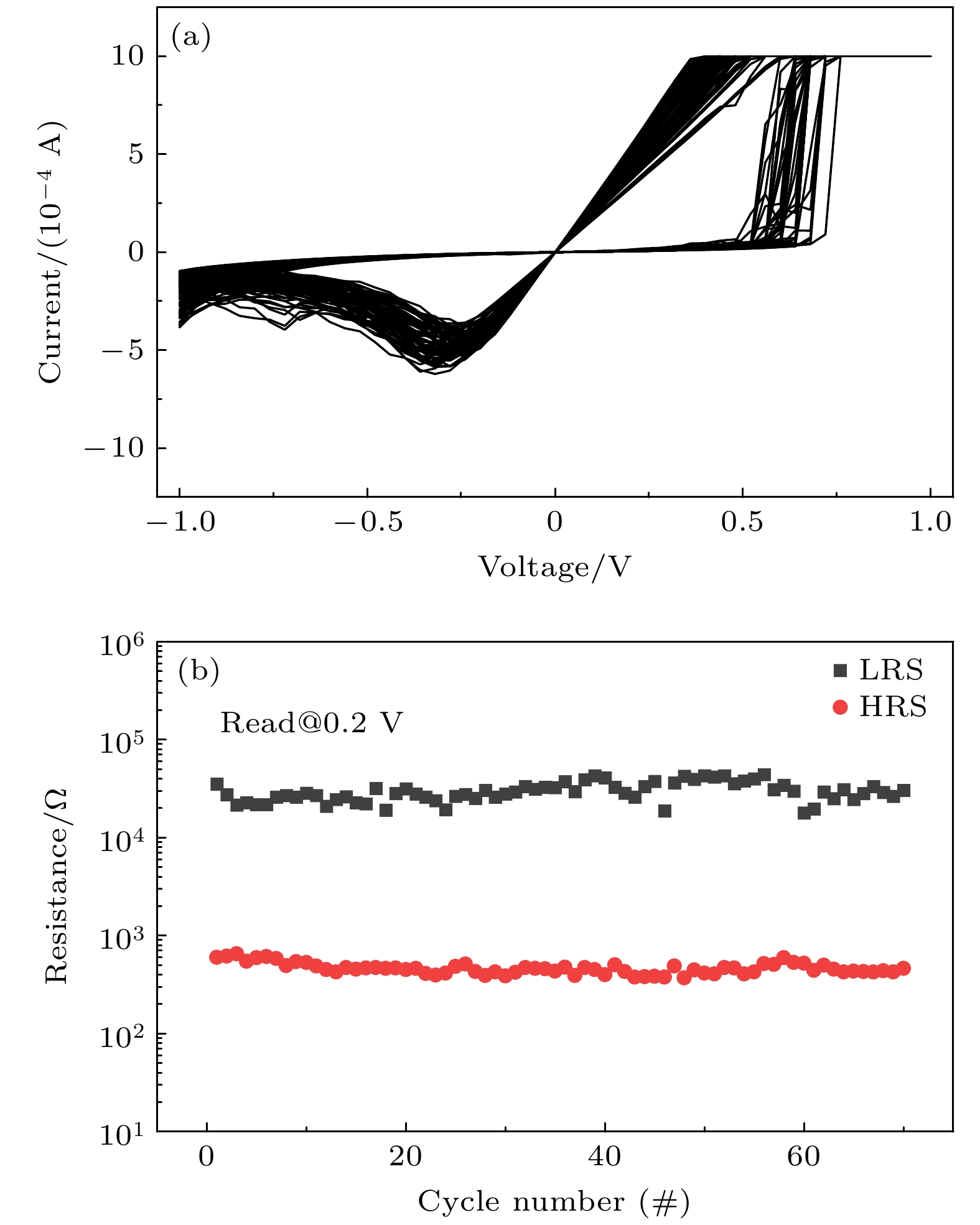
图 4 Fe2O3层厚约为100 nm的BFO/Fe2O3/ITO器件表现出优异的RS行为和稳定的NDR效应, 具有RRAM器件的潜力, 设备的稳定性是衡量设备性能的标准之一
Fig. 4. The BFO/Fe2O3/ITO device with ~100 nm-thick Fe2O3 layer demonstrates excellent resistive switching (RS) behavior and stable negative differential resistance (NDR) effect, indicating potential for RRAM applications. Device stability serves as a key performance metric.
-
[1] Weitz R T, Walter A, Engl R, Sezi R, Dehm C 2006 Nano Lett. 6 2810
Google Scholar
[2] Li X L, Jia J, Li Y C, Bai Y H, Li J, Shi Y N, Wang L F, Xu X H 2016 Sci. Rep. 6 31934
Google Scholar
[3] Bibes M, Barthélémy A 2008 Nat. Mater. 7 425
Google Scholar
[4] Miyake M, Scott J F, Lou X J, Morrison F D, Nonaka T, Motoyama S, Tatsuta T, Tsuji O 2008 J. Appl. Phys. 104 064112
Google Scholar
[5] Jensen W B 1997 J. Chem. Edu. 74 1063
Google Scholar
[6] Neale R G, Nelson D L, Moore G E 1970 Electronics 43 56
[7] Jeong D S, Thomas R, Katiyar R S, Scott J F, Kohlstedt H, Petraru A, Hwang C S 2012 Rep. Prog. Phys. 75 076502
Google Scholar
[8] Jeong D S, Choi B J, Hwang C S 2006 J. Appl. Phys. 100 113724
Google Scholar
[9] Yu S M, Guan X M, Wong H S P 2011 Appl. Phys. Lett. 99 063507
Google Scholar
[10] Hui F, Grustan-Gutierrez E, Long S B, Liu Q, Ott A K, Ferrari A C, Lanza M 2017 Adv. Electron. Mater. 3 1600195
Google Scholar
[11] Waser R 2012 J. Nanosci. Nanotechnol. 12 7628
Google Scholar
[12] Kim D C, Seo S, Ahn S E, Suh D S, Lee M J, Park B H, Yoo I K, Baek I G, Kim H J, Yim E K, Lee J E, Park S O, Kim H S, Chung U I, Moon J T, Ryu B I 2006 Appl. Phys. Lett. 88 202102
Google Scholar
[13] Mahapatra R, Maji S, Horsfall A B, Wright N G 2015 Microelectron. Eng. 138 118
Google Scholar
[14] Lee J S, Lee S, Noh T W 2015 App. Phys. Rev. 2 031303
Google Scholar
[15] Yoo H G, Kim S, Lee K J 2014 RSC Adv. 4 20017
Google Scholar
[16] Zhang W B, Wang C, Liu G, Wang J, Chen Y, Li R W 2014 Chem. Commun. 50 11496
Google Scholar
[17] He C T, Lu Y, Li X L, Chen P 2022 Acta Phys. Sin. 71 086102 [何朝滔, 卢羽, 李秀林, 陈鹏 2022 物理学报 71 086102]
Google Scholar
He C T, Lu Y, Li X L, Chen P 2022 Acta Phys. Sin. 71 086102
Google Scholar
[18] Zhang X W, He C T, Li X L, Qiu X Y, Zhang Y, Chen P 2022 Acta Phys. Sin. 71 187303 [张兴文, 何朝滔, 李秀林, 邱晓燕, 张耘, 陈鹏 2022 物理学报 71 187303]
Google Scholar
Zhang X W, He C T, Li X L, Qiu X Y, Zhang Y, Chen P 2022 Acta Phys. Sin. 71 187303
Google Scholar
[19] Guo T, Sun B, Zhou Y, Zhao H B, Lei M, Zhao Y 2018 PCCP 20 20635
Google Scholar
[20] Prakash C, Yadav A K, Dixit A 2023 Phys. Chem. Chem. Phys. 25 19868
Google Scholar
[21] Zhang K J, Ren K, Qin X Z, Zhu S H, Yang F, Zhao Y, Zhang Y 2021 IEEE Trans. Electron Dev. 68 3807
Google Scholar
[22] Kumar S, Strachan J P, Williams R S 2017 Nature 548 318
Google Scholar
[23] Kumar S, Williams R S, Wang Z 2020 Nature 585 518
Google Scholar
[24] Zhou G D, Gu D S, Ye J, Sun B, Shi H, Ran H, Ji'e M, Hu X, Wang L, Duan S, Ling H 2025 Adv. Mater. 37 e08107
Google Scholar
[25] Zhou G D, Duan S K, Li P, Sun B, Wu B, Yao Y Q, Yang X D, Han J J, Wu J G, Wang G, Liao L P, Lin C Y, Hu W, Xu C Y, Liu D B, Chen T, Chen L J, Zhou A K, Song Q L 2018 Adv. Electron. Mater. 4 1700567
Google Scholar
[26] Shuai Y, Zhou S Q, Bürger D, Helm M, Schmidt H 2011 J. Appl. Phys. 109 124117
Google Scholar
[27] Zheng P P, Sun B, Chen Y Z, Elshekh H, Yu T, Mao S S, Zhu S H, Wang H Y, Zhao Y, Yu Z 2019 Appl. Mater. Today 14 21
Google Scholar
[28] Lu Y, Tang Y Y, Li X L, He C T, Chen P 2022 App. Phys. A-Mater. 128 229
Google Scholar
[29] Tang M, Sun B, Huang J, Gao J, Li C M 2016 RSC Adv. 6 25028
Google Scholar

 下载:
下载:
计量
- 文章访问数: 808
- PDF下载量: 19
- 被引次数: 0
