


-
超导量子处理器芯片的制造工艺面临特殊的金属污染挑战, 其材料体系和工艺特性与传统半导体芯片存在显著差异. 本研究系统分析了量子芯片中金属污染的来源、扩散机制及防控策略, 重点探讨了超导材料(如Ta, Nb, Al, TiN等)在蓝宝石和硅衬底上的体扩散与表面迁移行为. 研究发现, 蓝宝石衬底因其致密晶格结构表现出优异的抗扩散性能, 而硅衬底需重点关注Au, In, Sn等易迁移金属的污染风险. 通过实验验证, Ti/Au结构的凸点下金属化层在硅衬底上易发生Au穿透扩散, 且增加Ti层厚度无法显著改善阻挡效果. 量子芯片的低温工艺(<250 ℃)和超低温工作环境(mK级)有效抑制了金属扩散, 但暴露的金属表面和材料多样性仍带来独特挑战. 研究建议建立量子芯片专属的金属污染防控体系, 并提出了后续在新型材料评估、表面态调控及长期可靠性研究等方向的发展路径. 本文为超导量子芯片的工艺优化和性能提升提供了重要理论支撑和技术指导.
The manufacturing process of superconducting quantum processor chips faces special challenges of metal contamination, and their material system and process characteristics are significantly different from those of traditional semiconductor chips. This study focuses on the issue of metal contamination in the fabrication process of quantum chips, systematically analyzing the sources, diffusion mechanisms, and prevention strategies of metal contamination in quantum chips, where the bulk diffusion and surface migration behaviors of superconducting materials (such as Ta, Nb, Al, TiN) on sapphire and silicon substrates are particularly emphasized, aiming to provide theoretical basis and technical references for process optimization and to promote the industrialization process of quantum computing technology. The metal contamination in the fabrication of quantum chips is mainly caused by the metal film materials used in the process, the external environment, or the unintended metal impurity atoms introduced in the manufacturing process. Among them, some quantum chip components directly use superconducting metal materials. Unlike semiconductor chips, they cannot achieve front and back stage isolation, resulting in the continuous presence of metal surface migration channels, and the exposed metal structures on the chip surface. Metal contamination often leads to two basic failure problems: short circuits and leakage currents. These problems mainly result from the bulk diffusion of metal impurities in the dielectric layer and the migration behavior on the sample surface. The diffusion and migration rates of metals are affected by temperature, interface reactions, defects, and grain boundaries. The results show that the sapphire substrate, due to its dense lattice structure, exhibits excellent anti-diffusion performance, reducing the risk of contamination and providing a stable interface environment for superconducting quantum chips. For silicon substrates, special attention must be paid to the contamination risks from high-mobility metals such as Au, In, and Sn. Experimental verification shows that Ti/Au under bump metallization structures on silicon substrates are prone to Au penetration diffusion, and increasing Ti thickness does not significantly improve the blocking effect. The low-temperature process (< 250 ℃) and ultra-low-temperature operating environment (mK level) of quantum chips effectively suppress metal diffusion, but the exposed metal surfaces and material diversity still pose unique challenges. The study recommends establishing a dedicated metal contamination prevention system for quantum chips and proposes future research directions, including the evaluations of novel materials, surface state regulation, and long-term reliability studies. This work provides important theoretical support and technical guidance for optimizing the process and enhancing the performance of superconducting quantum chips. -
Keywords:
- superconducting quantum processor chip /
- process line metal contamination /
- bulk diffusion /
- surface migration
-
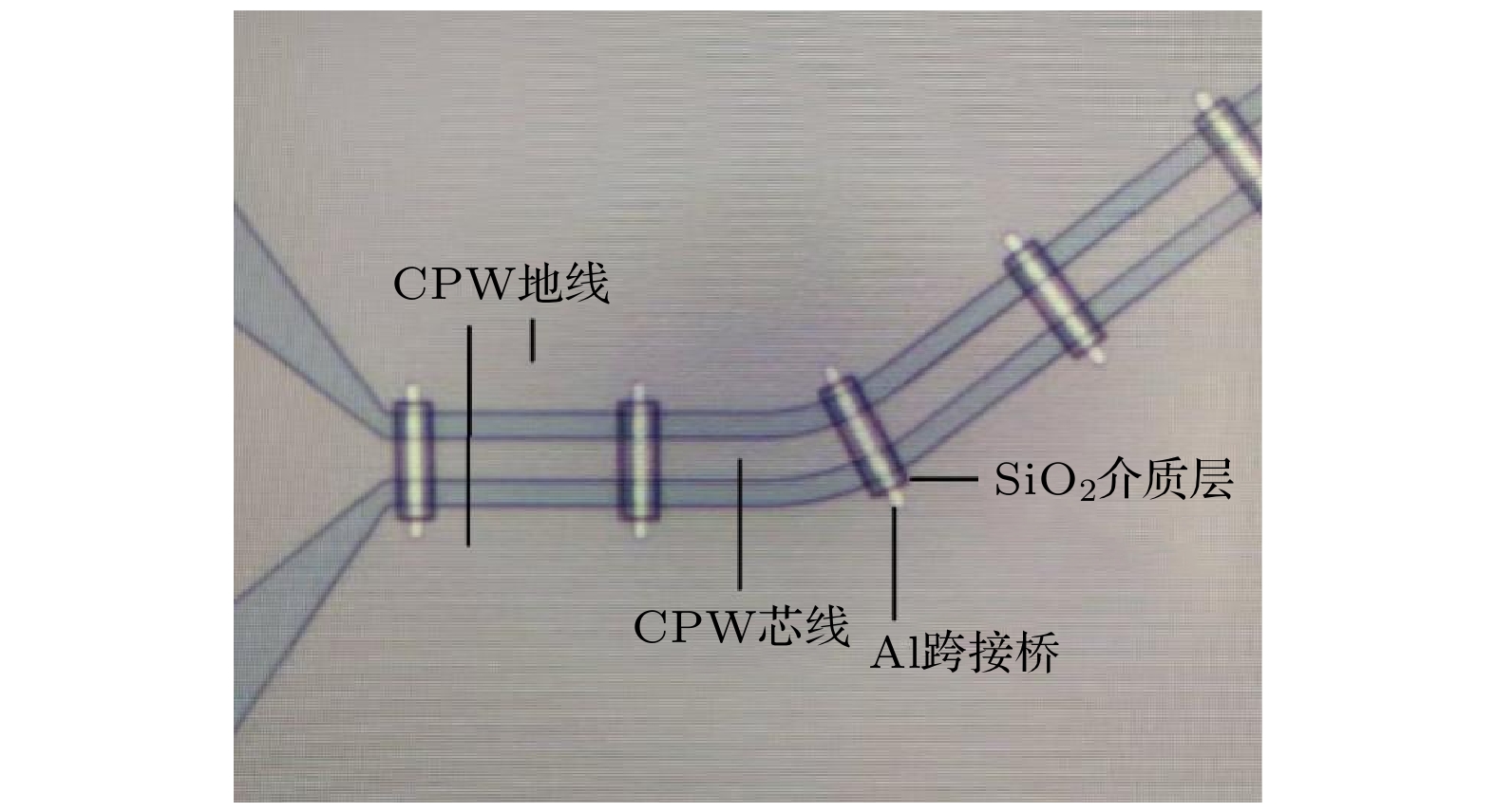
图 2 用于量子芯片的CPW传输线及其地线互连的铝质跨接桥结构
Fig. 2. Aluminum crossover bridge structure for CPW transmission line and ground interconnects in quantum chips.
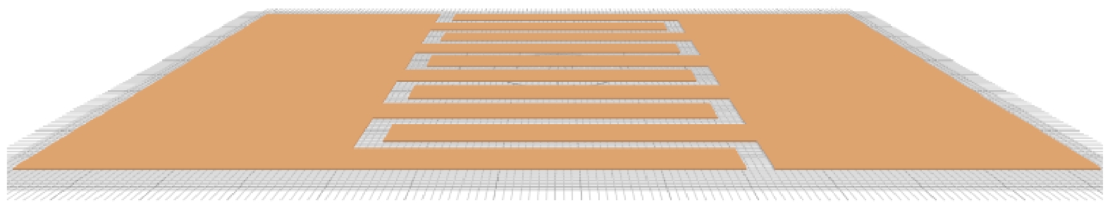
图 3 梳状电极UBM结构的线间电阻测试示意图
Fig. 3. Schematic of interline resistance test structure for comb-shaped UBM electrodes.
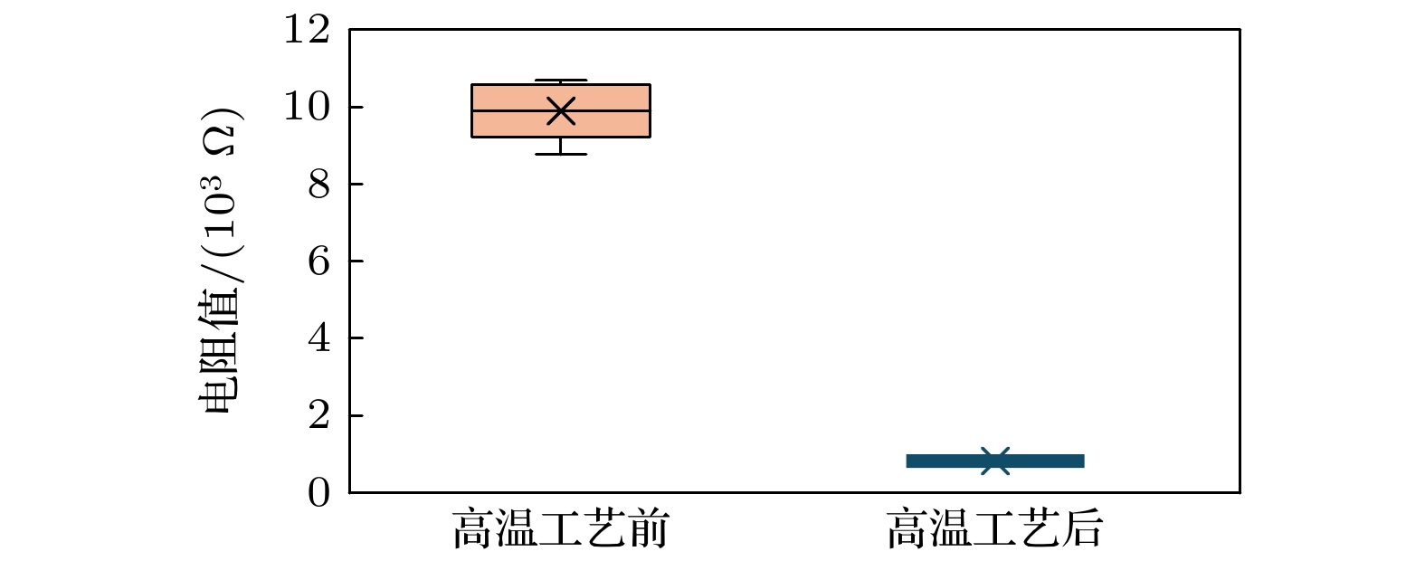
图 4 高温处理(245 ℃/5 min)前后UBM线间电阻变化对比
Fig. 4. Comparison of UBM interline resistance before and after thermal treatment (245 ℃/5 min).
表 1 半导体芯片与超导量子芯片的工艺比较
Table 1. Comparison of process characteristics between conventional semiconductor chips and superconducting quantum chips.
半导体芯片 超导量子芯片 器件 CMOS场效应晶体管等 约瑟夫森结的Transmon结构等 材料 衬底 Si, InP, SiC等 蓝宝石、高阻Si等 前道工艺 半导体掺杂等 超导金属、少量介质材料等 工艺 离子注入、热工艺等 有机清洗工艺、剥离工艺等 环境 温度 –40—150 ℃ 毫开尔文(mK)级低温 湿度 常规环境30%—70% RH或更宽泛 真空环境 电磁 常规环境
(除空间应用等特殊场景外)电磁屏蔽  下载: 导出CSV
-
[1] Acharya R, Abanin D A, Aghababaie-Beni L, Aleiner I, Andersen T I, Ansmann M, Arute F, Arya K, Asfaw A, Astrakhantsev N, et al. 2024 Nature 638 920
[2] Gao D X, Fan D J, Zha C, Bei J H, Cai G Q, Cai J B, Cao S R, Chen F S, Chen J, Chen K, et al. 2025 Phys. Rev. Lett. 134 090601
 Google Scholar
[3] Van Damme J, Massar S, Acharya R, Ivanov T, Perez Lozano D, Canvel Y, Demarets M, Vangoidsenhoven D, Hermans Y, Lai J G, Vadiraj A M, Mongillo M, Wan D, De Boeck J, Potočnik A, De Greve K 2024 Nature 634 74
Google Scholar
[4] Dieter K S 2005 Semiconductor Material and Device Characterization (Hoboken: Wiley IEEE Press) p127
[5] Weber E R 1983 Appl. Phys. A 30 1
Google Scholar
[6] 夸克M, 瑟达 J著(韩郑生译)2015 半导体制造技术(北京: 电子工业出版社)
Quirk M, Serda J (translated by Han Z S) 2015 Semiconductor Manufacturing Technology (Beijing: Publishing House of Electronics Industry
[7] Xiao H 2012 Introduction to Semiconductor Manufacturing Technology (Bellingham: SPIE Press
[8] Mehrer H 2007 Diffusion in Solids: Fundamentals, Methods, Materials, Diffusion-Controlled Processes (Heidelberg: Springer Verlag
[9] Seshan K 2012 Handbook of Thin Film Deposition: Techniques, Processes, and Technologies (Amsterdam: Elsevier
[10] Gas P, d'Heurle F M 1993 Appl. Surf. Sci. 73 153
Google Scholar
[11] Nicolet M A 1978 Thin Solid Films 52 415
Google Scholar
[12] Gösele U, Frank W, Seeger A 1980 Appl. Phys. 23 361
Google Scholar
[13] Nakashima K, Iwami M, Hiraki A 1975 Thin Solid Films 25 423
Google Scholar
[14] Murarka S P 2005 Diffusion Processes in Advanced Technological Materials (Amsterdam: Elsevier) pp239-281
[15] Saiz E, Cannon R M, Tomsia A P 1999 Acta Mater. 47 4209
Google Scholar
[16] Matthews T S, Sawyer C, Ogletree D F, Liliental-Weber Z, Chrzan D C, Wu J 2012 Phys. Rev. Lett. 108 096102
Google Scholar
[17] Prabriputaloong K, Piggott M R 1973 J. Am. Ceram. Soc. 56 177
Google Scholar
[18] Seebauer E G, Allen C E 1995 Prog. Surf. Sci. 49 265
Google Scholar
[19] Kirby K W 2008 M. S. Thesis(State College: The Pennsylvania State University
[20] Wu N J, Yasunaga H, Natori A 1992 Appl. Surf. Sci. 260 75
Google Scholar
[21] 李智瑞 2012 硕士学位论文 (北京: 北京化工大学)
Li Z R 2012 M. S. Thesis(Beijing: Beijing University of Chemical Technology
[22] 陆裕东, 何小琦, 恩云飞, 王歆, 庄志强 2010 物理学报 59 3438
Google Scholar
Lu Y D, He X Q, En Y F, Wang X, Zhuang Z Q 2010 Acta Phys. Sin. 59 3438
Google Scholar

 下载:
下载:
计量
- 文章访问数: 15
- PDF下载量: 0
- 被引次数: 0
