Search

Article

x

留言板

尊敬的读者、作者、审稿人, 关于本刊的投稿、审稿、编辑和出版的任何问题, 您可以本页添加留言。我们将尽快给您答复。谢谢您的支持!

姓名
邮箱
手机号码
标题
留言内容
验证码

Memory capacitance behavior at single resistance state in memristor and multi-state characteristic

Liu Ru-Xin Dong Rui-Xin Yan Xun-Ling Xiao Xia

Liu Ru-Xin, Dong Rui-Xin, Yan Xun-Ling, Xiao Xia. Memory capacitance behavior at single resistance state in memristor and multi-state characteristic. Acta Phys. Sin., 2019, 68(6): 068502. doi: 10.7498/aps.68.20181836
Citation:

Memory capacitance behavior at single resistance state in memristor and multi-state characteristic

Liu Ru-Xin, Dong Rui-Xin, Yan Xun-Ling, Xiao Xia
PDF
HTML
Get Citation
  • With the advent of the information age, big data put forward higher requirements for capacity of storage devices. Compared with the method of reducing the size of the device to enhance the integration level, the high density storage of increasing the memory state of the single device will be very beneficial to solving the problem. In this work, we propose an idea of two-parameter and multi-state memory device involved in both resistance and capacitance operation levels. At first, a new donor-acceptor (D-A)-type copolymer is designed and synthesized. Then, the memory device of Al/copolymer/ITO structure is fabricated, and the current-voltage (I-V) and capacitance-voltage (C-V) curves are measured by a KEITHLEY 4200 semiconductor characterization system. The device not only displays the obvious memory resistance characteristics, but also has the memory capacitance behavior in single resistance state, which results in two resistance states and four capacitance states, so that the device has the capability of two-parameter and multi-state memory. In addition, the device shows more capacitance states after the switching behavior has been modulated by the voltage amplitude, which provides an effective method to control the memory states. In order to study the conductive mechanism of the device, we test the relationship between resistance and temperature. It is found that the resistance decreases with the increase of temperature, indicating that the device has the obvious semiconductor properties. Furthermore, the fitting results of I-V data show that the mechanism of resistance switching is in good consistence with the classical trap-controlled space charge limited current theory. The capacitance switching in single resistance state is closely related to the polarization characteristic of D-A structure in the copolymer film. The polarization force microscopy phase image shows that the copolymer film has obvious polarization and depolarization characteristics under the external electric field. Based on the polarization characteristics of copolymer, the correlation between memory resistance and memory capacitance is established by introducing a polarization operator of molecules, and the matrix model describing the two-parameter and multi-state memory characteristics is given. The above results show that the multi-state memory characteristics will store more information than 2-bits mode in a single cell, which will provide a reference for improving the storage density of information.
      PACS:
      85.35.–p
      85.25.Hv(Superconducting logic elements and memory devices; microelectronic circuits)
      73.61.Ph(Polymers; organic compounds)
      77.22.Ej(Polarization and depolarization)
      Corresponding author: Dong Rui-Xin, ruixindong@163.com
    • Funds: Project supported by the National Natural Science Foundation of China (Grant No. 61574071) and the Special Construction Project Fund for Taishan Scholars of Shandong Province, China.

    忆阻器(memristor)由美国加州大学的Chua教授[1]根据电路理论的完备性提出, 惠普实验室[2]于2008年制备出第一个忆阻器件, 开创了忆阻器研究的先河. 由于忆阻器在非易失性存储[3-5]和神经突触模拟[6-8]方面均有潜在的应用价值, 所以国内外开展了许多相关的研究报道. 随着忆阻器的迅速发展, Ventra等[9]又从理论上定义了另外一种类型的记忆器件—忆容器(memcapacitor). 忆容器即具有记忆特性的电容开关器件, 因为其与忆阻器具有类似的记忆开关特性, 同时又能拓展器件的记忆参量, 因此忆容器也得到广泛研究[10,11]. Haik等[12]和Albamartin等[13]分别基于金属纳米颗粒和碳纳米管制备了记忆器件, 实现了电容的记忆开关特性, 这类电容记忆特性源于外界电场对嵌在两有机物层中的纳米结构的充放电效应. 值得注意的是, 2013年Yan和Liu[14]在多层金属氧化物器件中发现了电阻和电容开关的共存现象, 这种共存开关来源于Nb:SrTiO3/Au连接处的界面势垒效应. 随后, Salaoru等[15]实现了对电阻和电容共存开关的脉冲调控. 2016年, Park等[16]通过在有机物聚甲基丙烯酸甲酯(PMMA)层中嵌入石墨烯观察到了多级电阻和电容的共存开关现象, 此器件中石墨烯作为电荷的捕获与释放层, 重叠的PMMA/石墨烯结构使得器件具有多级电容状态. 上述研究使电阻和电容两个参量在同一个器件中得到了结合, 增加了存储参量. 但它们的共同特点是电阻和电容的开关具有同步性, 导致一种电阻状态仅对应一种电容状态, 限制了记忆状态的增加. 如果在同种电阻状态(高或低电阻态)下出现电容的开关行为, 器件的记忆状态将得到大幅度增加, 对于非易失性多态存储具有重要的意义.

    本文制备了具有Al/共聚物/ITO结构的有机记忆器件, 测试了其记忆电阻(忆阻)特性, 同时还研究了单个电阻状态下的记忆电容(忆容)行为, 发现器件存在两种电阻状态和与之对应的四种电容状态. 在此基础上对器件进行了电压幅值的调制, 器件展现了良好的电学可调控性能.

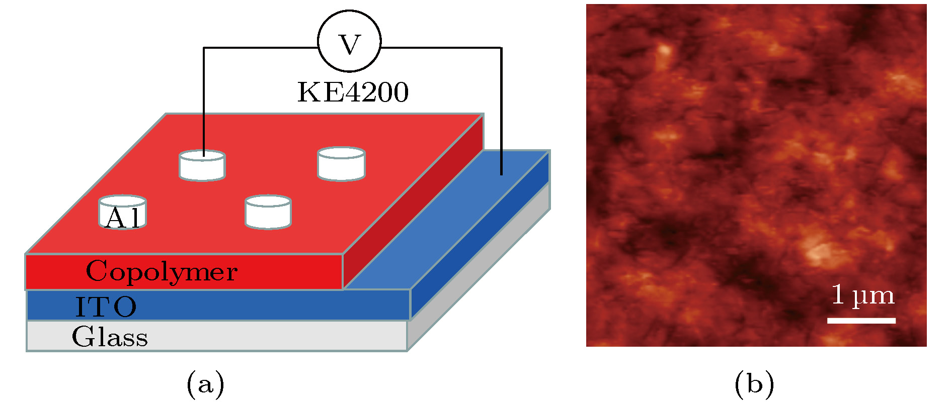
    器件的功能层为共聚物分子材料, 共聚物是利用具有强吸电子能力的苯并噻二唑单体作为电子受体、苯并二噻吩和咔唑作为供体合成的供体-受体类型的有机半导体材料. 首先, 将共聚物溶解在三氯甲烷溶剂中, 溶液的浓度为0.1 mg/mL. 溶液在室温下搅拌30 min后旋涂在清洗过的底电极ITO玻璃衬底上. 最后利用热蒸镀方法把直径为1.5 mm的点状铝电极沉积在共聚物薄膜上, 蒸镀真空度为5 × 10⁻⁴ Pa. 器件结构如图1(a)所示.

    图 1  (a)器件Al/共聚物/ITO的结构示意图; (b)薄膜表面的AFM图像, 扫描面积为5 ${\text{μ}} {\rm{m}}$ × 5 ${\text{μ}} {\rm{m}}$
    Fig. 1.  (a) Schematic of device with the Al/copolymer/ITO configuration; (b) AFM image of the copolymer film, with a scanning area of 5 ${\text{μ}} {\rm{m}}$ × 5 ${\text{μ}} {\rm{m}}$

    共聚物薄膜的表面形貌利用原子力显微镜(AFM; Solver-P47, NT-MDT)进行表征, 如图1(b)所示, 扫描范围为5 ${\text{μ}} {\rm{m}}$ × 5 ${\text{μ}} {\rm{m}}$. 分析得出: 薄膜表面的均方根粗糙度是5.6 nm, 说明有机薄膜层有较好的平整度, 保证了器件具有良好的稳定性. 共聚物薄膜的厚度利用台阶仪(Alpha-Step D-100, KLA-Tencor)测量, 膜厚为30 nm. 器件的电流-电压(I-V)和电容-电压(C-V)曲线通过半导体特性分析仪(4200-SCS, KEITHLEY)测量, 测量过程中ITO接地, 偏压施加到铝电极上. 共聚物薄膜的极化特性通过压电力显微镜(PFM; Dimension Icon, Bruker)进行测量, 测量过程中ITO接地, 偏压施加到薄膜上.

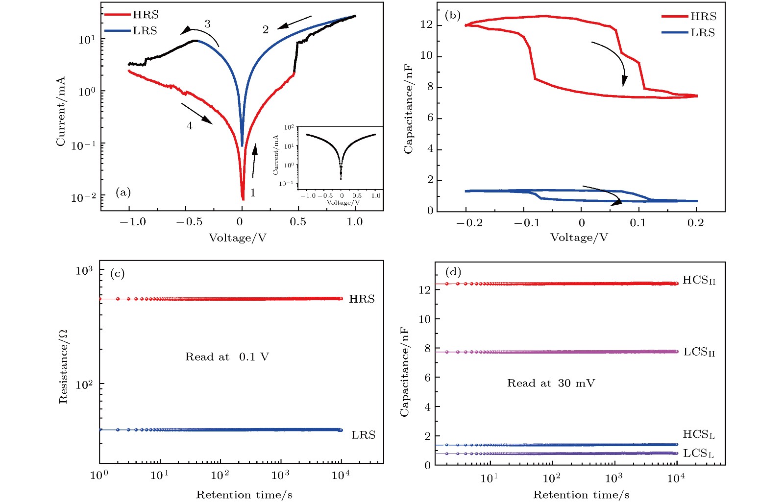
    图2(a)为器件Al/共聚物/ITO的I-V曲线, 电压的扫描范围是0 → 1 → –1 → 0 V, 从图中可以看出器件具有明显的忆阻行为. 最初, 器件处在高电阻状态(HRS), 并且在0 → 0.45 V内保持在HRS. 当电压超过0.45 V后, 随着电压的增大电流急剧增加, 0.45 V称为电阻的关闭电压($V_{\rm{OFF}}^R$). 器件在1 V处到达低电阻状态(LRS), 并且在1 → 0 → –0.5 V内保持在LRS. 当电压沿负方向继续增大时, 电流减小, 出现负微分电阻行为, –0.5 V称为电阻的开启电压($V_{\rm{ON}}^R$). 可以看出器件具有较小的开关电压, 有利于降低功耗. 当电压扫描到–1 V时, 器件回到最初的HRS. 在–0.1 V处读取的高、低电阻分别是550 和40 $\Omega $, 高-低电阻比约为14. 作为对比, 实验也对无共聚物层的Al/ITO器件进行了I-V曲线(图2(a)插图所示)测量, 没有发现电阻的开关现象, 说明电阻开关是由于嵌入到两电极中的有机层引起的.

    图 2  (a)器件Al/共聚物/ITO与Al/ITO(内插图)的I-V特性曲线, 红色和蓝色分别代表器件处在HRS和LRS; (b)器件Al/共聚物/ITO的C-V曲线, 红色和蓝色分别对应HRS和LRS下的C-V曲线; 扫描方向如图中箭头所示; 器件电阻(c)和电容(d)的时间保持特性
    Fig. 2.  (a) The I-V curves of Al/copolymer/ITO device. Inset is the Al/ ITO device. Red and blue curves represent HRS and LRS, respectively. (b) C-V curves of Al/copolymer/ITO device. Red and blue curves correspond to the C-V characteristics in HRS and LRS, respectively. The arrows show direction of voltage sweep. The retention time characteristics of resistance (c) and capacitance (d)

    为了研究单电阻状态下的忆容特性, 对器件的C-V曲线进行了测量(图2(b)所示), 扫描电压范围是–0.2 → +0.2 → –0.2 V, 电容的读取采用幅值30 mV、频率100 kHz的交流电压. 需要特别指出的是, ±0.2 V低于电阻的开关电压保证了电容测量是在同一种电阻状态下进行的.

    图2(b)的红线为HRS下的C-V特性曲线, 器件展现出顺时针的电容滞回特性. 起初, –0.2 V的扫描电压使器件处于高电容状态(HCS), 并且在–0.20 → 0.06 V区域内保持在HCS; 随着电压的增大电容不断减小, 在0.2 V处器件达到低电容状态(LCS), 并且一直保持在LCS, 直到–0.08 V; 当电压超过–0.08 V后, 器件的电容随着电压的升高不断增大, 在–0.2 V处器件又回到了HCS, 因此–0.08 和0.06 V分别称为器件电容的开启、关闭电压($V_{{\rm{ON}}}^C$$V_{{\rm{OFF}}}^C$). HRS下的高电容态(HCSH)和低电容态(LCSH)的电容分别是12.33和7.70 nF, 二者都是零偏压下读取的. 图2(b)中的蓝线为器件处于LRS下的C-V特性曲线, 与HRS下的C-V曲线具有类似的变化规律, 不同的是LRS下的高电容态(HCSL)和低电容态(LCSL)的电容值分别是1.36和0.71 nF.

    为了评估器件的稳定性, 测试了两种电阻和四种电容状态的时间保持特性, 结果如图2(c)图2(d)所示. 可以看出, 在104 s时间范围内, 器件的电阻和电容状态基本保持不变. 并且从数据的变化趋势看, 可保持时间会更长, 意味着器件具有良好的时间保持特性, 同时也说明电阻和电容的多态行为具有非挥发性.

    与文献[1416]的结果相比, 本文中的电容开关发生在同种电阻状态下, 器件存在两种电阻态(HRS和LRS)和与之对应的四种电容态(HCSH, LCSH, HCSL和LCSL), 意味着器件可以实现电阻和电容的双参量记忆特性. 如果把这些电阻和电容状态编码为多级存储状态, 则可以有效增加单个元件的信息存储密度.

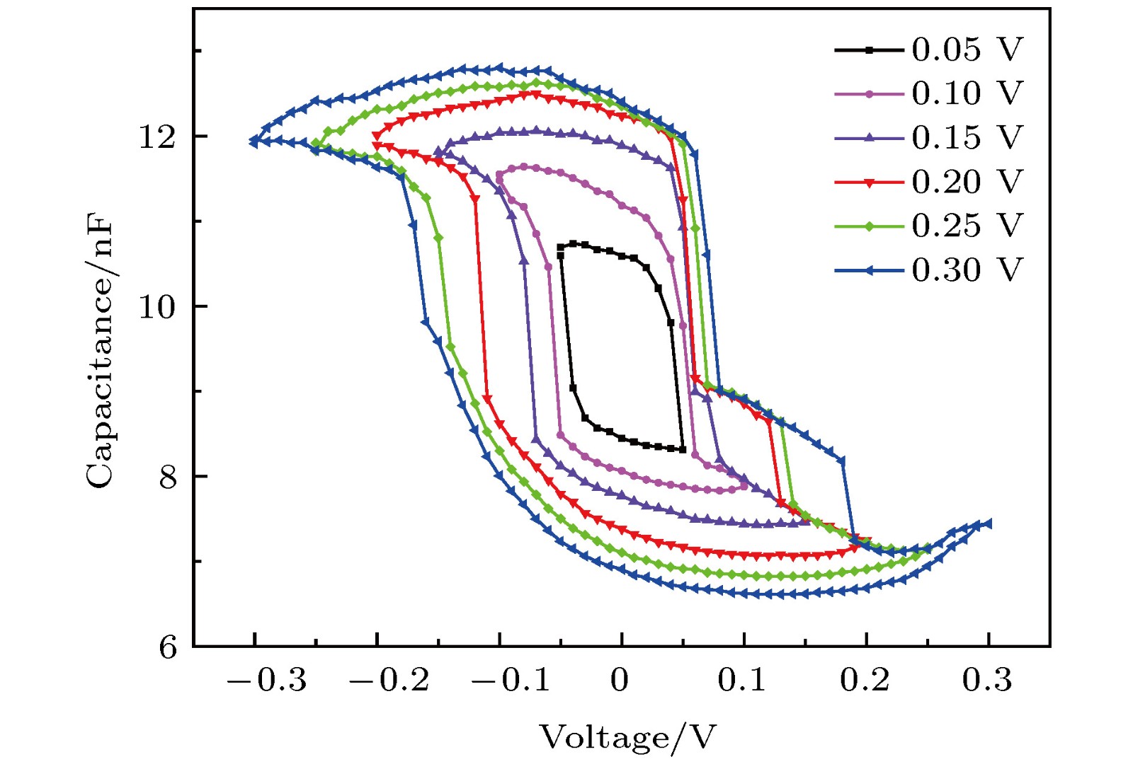
    图3给出了器件处于HRS时, 不同幅值的直流扫描电压对器件电容特性调制的结果, 电压幅值分别为0.05, 0.10, 0.15, 0.20, 0.25和0.30 V. 测量发现, 随着电压幅值的增大, 电容的开关电压随之增大, 高、低电容之间的窗口面积也越来越大(LRS下的规律类似). 这种现象归因于器件内部的极化强度随外电场的改变, 随着扫描电压的增大, 器件的极化与退极化程度也增强, 使薄膜内部发生分离和复位的正负电荷增加, 从而出现更明显的电容开关行为. 在调制过程中, 不同幅值的直流扫描电压使器件出现多种不同的电容开关行为, 从而增加了同种电阻状态下的电容状态, 意味着器件具有更多可利用的信息存储状态, 对于实现信息的高密度存储具有重要意义.

    图 3  高阻态中不同扫描电压幅值下的C-V曲线(交流读取电压为30 mV, 100 kHz)
    Fig. 3.  The C-V curves of HRS under the different sweep voltage (AC read voltage 30 mV, 100 kHz)
    3.3.1   忆阻特性的开关机理

    器件高、低电阻随温度的变化规律可以反映出器件的导电属性和开关机理, 因此对高、低电阻随温度的变化规律进行了研究, 结果如图4(a)图4(b)所示. 可以看出, 电阻与温度有很强的关联性, 两种阻态下的电阻均随温度的升高而明显减小, 显示出半导体属性[17]. 因此也排除了以下两种导电丝通道的可能: 若电阻的开关源于完全导电丝通道的形成和断裂, 那么低阻态下的电阻会存在典型的金属行为, 即电阻随着温度的升高而线性增加[18]; 若源于非完全导电通道, 那么低阻态的电阻会存在典型的电子隧穿行为, 电阻随温度的升高而微弱减小[19].

    图 4  在高(a)、低(b)阻态下器件的电阻随温度的变化; (c)正电压区域和(d)负电压区域器件的双对数I-V曲线, 图中已标出了每段的斜率
    Fig. 4.  Resistance versus temperature plots for the device in HRS (a) and LRS (b). Double-logarithmic I-V curves of the device: exerted (c) positive voltage or (d) negative voltage, and the value of the slope is marked in the figure

    为了进一步研究器件忆阻特性的开关机理, 根据图2(a)I-V数据给出了双对数曲线, 如图4(c)图4(d)所示. 图4(c)为正向电压区域的拟合结果, 器件在0 → 0.3 V内符合欧姆行为(I$\propto $V), 这是由于电压较小时注入的载流子较少, 大部分被缺陷捕获, 只有小部分载流子参与导电, 此时电流较小. 在0.3 → 0.45 V区域内, 随着电压的增大, 注入的载流子增多, 被捕获的比例减少, 更多的载流子参与导电, 电流明显增大, 符合Mott-Gurney law (I$\propto $V2). 当V > 0.45 V时, 器件中的缺陷被填满, 注入的载流子几乎都参与了导电, 薄膜具有更好的导电能力, 器件由HRS转变为LRS. 上述拟合结果与讨论说明高、低电阻状态的载流子传输行为符合空间电荷限制电流理论[20-22], 空间电荷限制电流主要由薄膜中的缺陷控制, 这些缺陷一方面源于薄膜的制备过程, 另一方面共聚物链上的化学基团也可扮演缺陷角色[23]. 在1→ 0 V区域, 由于之前的扫描过程已经完成了缺陷的填充所以器件仍处于LRS. 当给器件施加负偏压时, 在–0.5—1 V区域内, 随着偏压的增大电流反而减小, 器件出现负微分电阻效应, 如图4(d)所示. 这主要是因为在反向电场作用下缺陷中的载流子逐渐脱陷[24], 缺陷使载流子的传输受阻, 器件逐渐由LRS回到HRS. 因此, 器件的忆阻行为可视为共聚物薄膜中的缺陷对载流子的捕获和释放.

    3.3.2   忆容特性的开关机理

    为了研究忆容的开关机理, 利用PFM对共聚物薄膜进行了极化测量, 结果如图5所示. 相位图显示出三个明显的区域, 区域Ⅰ是负偏压下的极化结果, 区域Ⅱ是正偏压下的退极化结果, 对比发现薄膜在正负电场作用下发生了明显的极化与退极化. 区域Ⅲ是负偏压下再次极化的结果, 说明这种极化过程是可逆的. 正是因为共聚物薄膜具有可逆的极化与退极化特性, 使Al/共聚物/ITO器件表现出忆容开关行为.

    图 5  共聚物薄膜的PFM相位图, 其中首先对5 ${\text{μ}} {\rm{m}}$ × 5 ${\text{μ}} {\rm{m}}$区域的薄膜施加–10 V的偏压, 然后对内部的3.5 ${\text{μ}} {\rm{m}}$ × 3.5 ${\text{μ}} {\rm{m}}$区域施加+10 V的偏压, 再对中心的1.5 ${\text{μ}} {\rm{m}}$ × 1.5 ${\text{μ}} {\rm{m}}$区域施加–10 V的偏压, 最后通过15 mV的交变信号对5 ${\text{μ}} {\rm{m}}$ × 5 ${\text{μ}} {\rm{m}}$薄膜的极化程度进行测量
    Fig. 5.  The PFM phase image of the copolymer film. First, an external voltage of –10 V was applied to a square of 5 ${\text{μ}} {\rm{m}}$ × 5 ${\text{μ}} {\rm{m}}$. Secondly, +10 V was applied to a square of 3.5 ${\text{μ}} {\rm{m}}$ × 3.5 ${\text{μ}} {\rm{m}}$, and then –10 V was applied to a square of 1.5 ${\text{μ}} {\rm{m}}$ × 1.5 ${\text{μ}} {\rm{m}}$. Finally, the polarization degree of 5 ${\text{μ}} {\rm{m}}$ × 5 ${\text{μ}} {\rm{m}}$ film was measured by 15 mV alternating signal.

    共聚物薄膜之所以表现出这种极化特性是与共聚物分子的供体-受体结构密切相关的, 苯并噻二唑是强电子接收单元, 苯并二噻吩和咔唑是两个电子提供单元[25,26], 所以分子的极化和退极化过程很容易在电场作用下实现. 当外部的负电压作用在器件上时, 内部的分子基团被极化, 正负电荷发生相对位移. 这个过程类似于等量的异号电荷分布在平行板电容器的两个极板上, 对应于器件的HCS. 反之, 当反向偏压施加到器件上时, 极化的分子出现退极化现象, 发生相对位移的正负电荷又会重新复位, 和电容器两极板的等量异号电荷发生中和类似, 对应于器件的LCS.

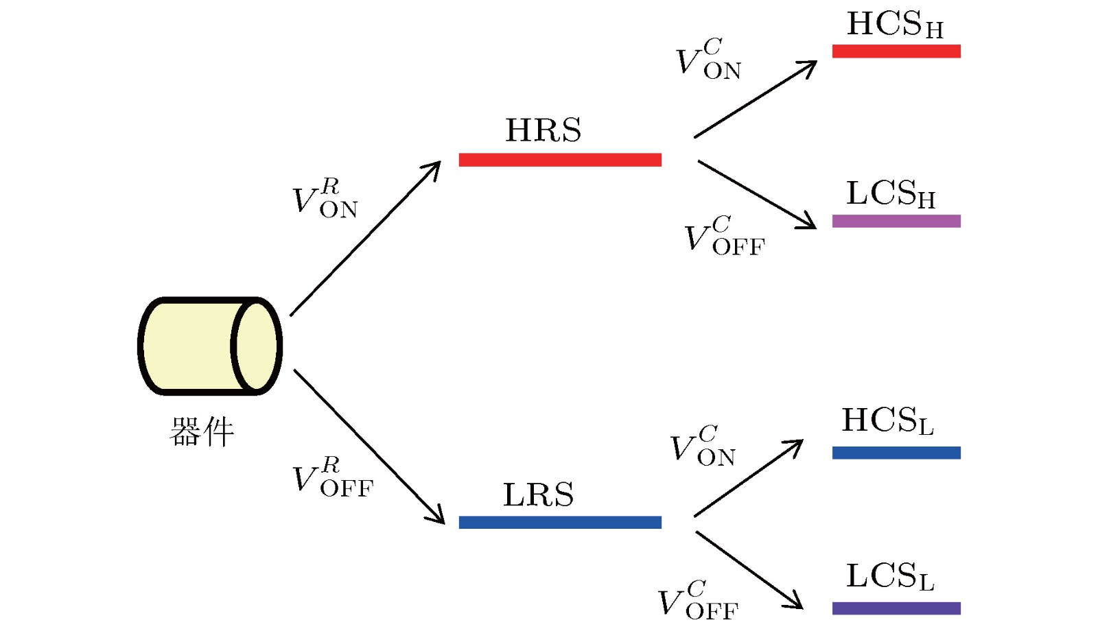
    器件单电阻态下的电容开关及其多态行为可以通过图6的模型示意图进行说明. 通过施加一个电阻的开/关电压($V_{\rm{ON}}^R/V_{\rm{OFF}}^R$), 器件会出现对应的高/低电阻状态(${\rm{HRS}}/{\rm{LRS}}$); 在确定的高(或低)电阻状态下, 再施加一个电容的开/关电压($V_{\rm{ON}}^C/V_{\rm{OFF}}^C$), 有机薄膜会发生极化/退极化行为, 使器件呈现出高/低电容状态(${\rm{HC}}{{\rm{S}}_{\rm{H}}}/{\rm{LC}}{{\rm{S}}_{\rm{H}}}$) (或${\rm{HC}}{{\rm{S}}_{\rm{L}}}/{\rm{LC}}{{\rm{S}}_{\rm{L}}}$).

    图 6  器件中电阻开关及单电阻态下的电容开关模型示意图
    Fig. 6.  Model schematic of resistance switching and capacitance switching at single resistance state in the device

    为了更好地理解忆阻和忆容的关联性以及多态特征, 本文给出一个矩阵模型来描述图2中的I-VC-V曲线中的电学特性. I-V曲线中的高、低电阻特征态分别表示为 ${{{\varPhi }}_1} = {\left(\!\! {{array}{*{20}{c}} 1 \\ 0 {array}} \!\!\right)_R}$${{{\varPhi }}_2} = {\left(\!\! {{array}{*{20}{c}} 0 \\ { - 1} {array}} \!\!\right)_R}$, $\hat R$表示电阻算符, 则电阻的测量操作表示为

    $\hat R{{{\varPhi }}_m} = {R_m}{{{\varPhi }}_m},\;\;\;m = 1,\;2.$

    (1)

    在电阻的关闭电压$V_{\rm{OFF}}^R$作用下器件从HRS向LRS转变, 与图2(a)中的电阻关的过程对应, 这个过程通过幺正变换描述为

    $\hat U_{\rm{OFF}}^R{{{\varPhi }}_1} = \left( \!\!{\begin{array}{*{20}{c}} 0&1 \\ { - 1}&0 \end{array}} \!\!\right){\left( \!\!{\begin{array}{*{20}{c}} 1 \\ 0 \end{array}} \!\!\right)_R} = {\left( \!\!{\begin{array}{*{20}{c}} 0 \\ { - 1} \end{array}} \!\!\right)_R} = {{{\varPhi }}_2}.$

    (2)

    反之, 器件在电阻的开启电压$V_{\rm{ON}}^R$作用下从LRS向HRS转变, 此过程通过(2)式的逆变换来实现

    $\hat U_{\rm{ON}}^R{{{\varPhi }}_2} = \left( {\begin{array}{*{20}{c}} 0&{ - 1} \\ 1&0 \end{array}} \right){\left( {\begin{array}{*{20}{c}} 0 \\ { - 1} \end{array}} \right)_R} = {\left( {\begin{array}{*{20}{c}} 1 \\ 0 \end{array}} \right)_R} = {{{\varPhi }}_1}, $

    (3)

    其中幺正算符$\hat U_{\rm{OFF}}^R = \hat U{_{\rm{ON}}^{R - 1}}$.

    由于供体-受体分子在外加电场作用下会发生极化与退极化, 分子处于高、低极化状态分别对应于器件的高、低电容. 设供体-受体分子的极化强度算符为$\hat P = \left( {{array}{*{20}{c}}{{P_1}} & 0\\0 & {{P_2}}{array}} \right)$, 则

    $\hat P{{{X}}_k} = {P_k}{{{X}}_k},\;\;\;k = 1,\;2,$

    (4)

    其中Pk为极化算符的本征值(极化强度), 且为开关电压的函数; ${{{X}}_1} = \left( {array}{l}1\\0{array} \right)$${{{X}}_2} = \left( {array}{l}0\\ - 1{array} \right)$分别表示分子的高、低极化态. 低极化状态的分子在电容的开启电压$V_{\rm{ON}}^C$作用下发生极化, 逐渐向高极化态转变, 对应于图2(b)C-V曲线的低→高电容的转变过程, 这个过程通过幺正变换描述为

    $\hat U_{\rm{ON}}^C{{{X}}_2} = \left( {\begin{array}{*{20}{c}} 0&{ - 1} \\ 1&0 \end{array}} \right)\left( {\begin{array}{*{20}{c}} 0 \\ { - 1} \end{array}} \right) = \left( {\begin{array}{*{20}{c}} 1 \\ 0 \end{array}} \right).$

    (5)

    反之, 分子在电容的关闭电压$V_{\rm{OFF}}^C$作用下发生退极化, 从高极化态转变为低极化态, 此过程通过(5)式中的逆变换来实现

    $\hat U_{\rm{OFF}}^C{{{X}}_1} = \left( {\begin{array}{*{20}{c}} 0&1 \\ { - 1}&0 \end{array}} \right)\left( {\begin{array}{*{20}{c}} 1 \\ 0 \end{array}} \right) = \left( {\begin{array}{*{20}{c}} 0 \\ { - 1} \end{array}} \right), $

    (6)

    其中幺正算符$\hat U_{\rm{OFF}}^C = \hat U{_{\rm{ON}}^{C- 1}}$.

    电容态由电阻和内部极化状态确定, 它们之间的关系可表示为

    $\hat C = \hat R\hat P =\left( {\begin{array}{*{20}{c}} {{R_{\rm{L}}}} & 0\\ 0 & {{R_{\rm{H}}}} \end{array}} \right) \otimes \left( {\begin{array}{*{20}{c}} {{P_1}} & 0\\ 0 & {{P_2}} \end{array}} \right),$

    (7)

    其中$\hat C$表示电容的测量算符. 电容的测量操作表示为

    $ \begin{aligned} \hat C{ \varPsi _n} = \hat R{ \varPhi _m}\hat P{X_k} = {R_m}{ \varPhi _m}{P_k}{X_k} = {C_n}{ \varPsi _n},\;\;\; \hfill \\ n = 1,\;2,\;3,\;4, \;\;\; \;\;\; \;\;\; \hfill \\ \end{aligned} $

    (8)

    这里Cn${{\varPsi} _n}$分别表示电容算符的本征值(实验测量值)与本征函数; C1, C2C3, C4分别表示LRS和HRS下的高、低电容.

    可见, 上述理论模型通过引入一个分子内部极化算符, 建立了忆阻和忆容的关联性, 较好地描述了器件的双参量多状态特征.

    本文制备了Al/共聚物/ITO 结构的有机记忆器件. 该器件展现了忆阻和忆容的共存现象, 特别是在高/低电阻状态下均发现了电容的开关行为, 使器件实现电阻和电容的双参量记忆特性的同时增加了记忆状态, 有利于增加单个元件的信息存储密度. 另外, 器件还实现了记忆电容特性的电压幅值调制, 使同种电阻状态下出现了更多的电容状态, 可更有效地提高信息的存储密度. 最后, 根据分子的结构特点, 引入内部极化算符, 建立了描述忆阻和忆容关联性的矩阵模型, 揭示了器件的双参量多状态特征.

    感谢聊城大学化学化工学院的赵金生教授在材料合成方面给予的宝贵帮助.

    [1]

    Chua L O 1971 IEEE Trans. Circuit Theory 18 507Google Scholar

    [2]

    Strukov D B, Snider G S, Stewart D R, Williams R S 2008 Nature 453 80Google Scholar

    [3]

    王媛, 董瑞新, 闫循领 2015 物理学报 64 048402Google Scholar

    Wang Y, Dong R X, Yan X L 2015 Acta Phys. Sin. 64 048402Google Scholar

    [4]

    Wang M, Cai S H, Pan C, Wang C Y, Lian X J, Zhuo Y, Xu K, Cao T J, Pan X Q, Wang B G, Liang S J, Yang J J, Wang P, Miao F 2018 Nat. Electron. 1 130Google Scholar

    [5]

    余志强, 刘敏丽, 郎建勋, 钱楷, 张昌华 2018 物理学报 67 157302Google Scholar

    Yu Z Q, Liu M L, Lang J X, Qian K, Zhang C H 2018 Acta Phys. Sin. 67 157302Google Scholar

    [6]

    Banerjee W, Liu Q, Lv H, Long S, Liu M 2017 Nanoscale 9 14442Google Scholar

    [7]

    Yan X, Wang J, Zhao M, Li X, Wang H, Zhang L, Lu C, Ren D 2018 Appl. Phys. Lett. 113 013503Google Scholar

    [8]

    Wang L Y, Wang Z Y, Zhao W, Hu B, Xie L H, Yi M D, Ling H F, Zhang C X, Chen Y, Lin J Y, Zhu J L, Huang W 2017 Adv. Electron. Mater. 3 1600244Google Scholar

    [9]

    Ventra M D, Pershin Y V, Chua L O 2009 Proc. IEEE 97 1717Google Scholar

    [10]

    Pershin Y V, Di Ventra M 2011 Adv. Phys. 60 145Google Scholar

    [11]

    Bessonov A A, Kirikova M N, Petukhov D I, Allen M, Ryhänen T, Bailey M J A 2015 Nat. Mater. 14 199Google Scholar

    [12]

    Haik M Y, Ayesh A I, Abdulrehman T, Haik Y 2014 Mater. Lett. 124 67Google Scholar

    [13]

    Albamartin M, Firmager T, Atherton J, Rosamond M C, Ashall D, Ghaferi A A, Ayesh A, Gallant A J, Mabrook M F, Petty M C, Zeze D A 2012 J. Phys. D: Appl. Phys. 45 295401Google Scholar

    [14]

    Yan Z B, Liu J M 2013 Sci. Rep. 3 2482Google Scholar

    [15]

    Salaoru I, Khiat A, Li Q, Berdan R, Prodromakis T 2013 Appl. Phys. Lett. 103 233513Google Scholar

    [16]

    Park M, Park S, Yoo K H 2016 ACS Appl. Mater. Interfaces 8 14046Google Scholar

    [17]

    Pan R B, Li J, Zhuge F, Zhu L Q, Liang L Y, Zhang H L, Gao J H, Cao H T, Fu B, Li K 2016 Appl. Phys. Lett. 108 013504Google Scholar

    [18]

    Hu L X, Fu S, Chen Y H, Cao H T, Liang L Y, Zhang H L, Gao J H, Wang J R, Zhuge F 2017 Adv. Mater. 29 1606927Google Scholar

    [19]

    Menzel S, Bottger U, Waser R 2012 J. Appl. Phys. 111 014501Google Scholar

    [20]

    Fujii T, Kawasaki M, Sawa A, Akoh H, Kawazoe Y, Tokura Y 2005 Appl. Phys. Lett. 86 012107Google Scholar

    [21]

    Ko Y, Kim Y, Baek H, Cho J 2011 ACS Nano 5 9918Google Scholar

    [22]

    Sun Y, Ai C, Lu J, Li L, Wen D, Bai X 2016 Thin Solid Films 598 293Google Scholar

    [23]

    Wang H, Meng F B, Cai Y R, Zheng L Y, Li Y G , Liu Y J , Jiang Y Y, Wang X T, Chen X D 2013 Adv. Mater. 25 5498Google Scholar

    [24]

    Mohanta K, Majee S K, Batabyal S K, Pal A J 2006 J. Phys. Chem. B 110 18231Google Scholar

    [25]

    Zhang Y, Kong L, Ju X, Zhao J 2017 Polymers 10 23Google Scholar

    [26]

    Irgashev R A, Teslenko A Y, Zhilina E F, Schepochkin A V, El'Tsov O S, Rusinov G L, Charushin V N 2014 Tetrahedron 70 4685Google Scholar

    期刊类型引用(0)

    其他类型引用(1)

  • 图 1  (a)器件Al/共聚物/ITO的结构示意图; (b)薄膜表面的AFM图像, 扫描面积为5 ${\text{μ}} {\rm{m}}$ × 5 ${\text{μ}} {\rm{m}}$

    Figure 1.  (a) Schematic of device with the Al/copolymer/ITO configuration; (b) AFM image of the copolymer film, with a scanning area of 5 ${\text{μ}} {\rm{m}}$ × 5 ${\text{μ}} {\rm{m}}$

    图 2  (a)器件Al/共聚物/ITO与Al/ITO(内插图)的I-V特性曲线, 红色和蓝色分别代表器件处在HRS和LRS; (b)器件Al/共聚物/ITO的C-V曲线, 红色和蓝色分别对应HRS和LRS下的C-V曲线; 扫描方向如图中箭头所示; 器件电阻(c)和电容(d)的时间保持特性

    Figure 2.  (a) The I-V curves of Al/copolymer/ITO device. Inset is the Al/ ITO device. Red and blue curves represent HRS and LRS, respectively. (b) C-V curves of Al/copolymer/ITO device. Red and blue curves correspond to the C-V characteristics in HRS and LRS, respectively. The arrows show direction of voltage sweep. The retention time characteristics of resistance (c) and capacitance (d)

    图 3  高阻态中不同扫描电压幅值下的C-V曲线(交流读取电压为30 mV, 100 kHz)

    Figure 3.  The C-V curves of HRS under the different sweep voltage (AC read voltage 30 mV, 100 kHz)

    图 4  在高(a)、低(b)阻态下器件的电阻随温度的变化; (c)正电压区域和(d)负电压区域器件的双对数I-V曲线, 图中已标出了每段的斜率

    Figure 4.  Resistance versus temperature plots for the device in HRS (a) and LRS (b). Double-logarithmic I-V curves of the device: exerted (c) positive voltage or (d) negative voltage, and the value of the slope is marked in the figure

    图 5  共聚物薄膜的PFM相位图, 其中首先对5 ${\text{μ}} {\rm{m}}$ × 5 ${\text{μ}} {\rm{m}}$区域的薄膜施加–10 V的偏压, 然后对内部的3.5 ${\text{μ}} {\rm{m}}$ × 3.5 ${\text{μ}} {\rm{m}}$区域施加+10 V的偏压, 再对中心的1.5 ${\text{μ}} {\rm{m}}$ × 1.5 ${\text{μ}} {\rm{m}}$区域施加–10 V的偏压, 最后通过15 mV的交变信号对5 ${\text{μ}} {\rm{m}}$ × 5 ${\text{μ}} {\rm{m}}$薄膜的极化程度进行测量

    Figure 5.  The PFM phase image of the copolymer film. First, an external voltage of –10 V was applied to a square of 5 ${\text{μ}} {\rm{m}}$ × 5 ${\text{μ}} {\rm{m}}$. Secondly, +10 V was applied to a square of 3.5 ${\text{μ}} {\rm{m}}$ × 3.5 ${\text{μ}} {\rm{m}}$, and then –10 V was applied to a square of 1.5 ${\text{μ}} {\rm{m}}$ × 1.5 ${\text{μ}} {\rm{m}}$. Finally, the polarization degree of 5 ${\text{μ}} {\rm{m}}$ × 5 ${\text{μ}} {\rm{m}}$ film was measured by 15 mV alternating signal.

    图 6  器件中电阻开关及单电阻态下的电容开关模型示意图

    Figure 6.  Model schematic of resistance switching and capacitance switching at single resistance state in the device

  • [1]

    Chua L O 1971 IEEE Trans. Circuit Theory 18 507Google Scholar

    [2]

    Strukov D B, Snider G S, Stewart D R, Williams R S 2008 Nature 453 80Google Scholar

    [3]

    王媛, 董瑞新, 闫循领 2015 物理学报 64 048402Google Scholar

    Wang Y, Dong R X, Yan X L 2015 Acta Phys. Sin. 64 048402Google Scholar

    [4]

    Wang M, Cai S H, Pan C, Wang C Y, Lian X J, Zhuo Y, Xu K, Cao T J, Pan X Q, Wang B G, Liang S J, Yang J J, Wang P, Miao F 2018 Nat. Electron. 1 130Google Scholar

    [5]

    余志强, 刘敏丽, 郎建勋, 钱楷, 张昌华 2018 物理学报 67 157302Google Scholar

    Yu Z Q, Liu M L, Lang J X, Qian K, Zhang C H 2018 Acta Phys. Sin. 67 157302Google Scholar

    [6]

    Banerjee W, Liu Q, Lv H, Long S, Liu M 2017 Nanoscale 9 14442Google Scholar

    [7]

    Yan X, Wang J, Zhao M, Li X, Wang H, Zhang L, Lu C, Ren D 2018 Appl. Phys. Lett. 113 013503Google Scholar

    [8]

    Wang L Y, Wang Z Y, Zhao W, Hu B, Xie L H, Yi M D, Ling H F, Zhang C X, Chen Y, Lin J Y, Zhu J L, Huang W 2017 Adv. Electron. Mater. 3 1600244Google Scholar

    [9]

    Ventra M D, Pershin Y V, Chua L O 2009 Proc. IEEE 97 1717Google Scholar

    [10]

    Pershin Y V, Di Ventra M 2011 Adv. Phys. 60 145Google Scholar

    [11]

    Bessonov A A, Kirikova M N, Petukhov D I, Allen M, Ryhänen T, Bailey M J A 2015 Nat. Mater. 14 199Google Scholar

    [12]

    Haik M Y, Ayesh A I, Abdulrehman T, Haik Y 2014 Mater. Lett. 124 67Google Scholar

    [13]

    Albamartin M, Firmager T, Atherton J, Rosamond M C, Ashall D, Ghaferi A A, Ayesh A, Gallant A J, Mabrook M F, Petty M C, Zeze D A 2012 J. Phys. D: Appl. Phys. 45 295401Google Scholar

    [14]

    Yan Z B, Liu J M 2013 Sci. Rep. 3 2482Google Scholar

    [15]

    Salaoru I, Khiat A, Li Q, Berdan R, Prodromakis T 2013 Appl. Phys. Lett. 103 233513Google Scholar

    [16]

    Park M, Park S, Yoo K H 2016 ACS Appl. Mater. Interfaces 8 14046Google Scholar

    [17]

    Pan R B, Li J, Zhuge F, Zhu L Q, Liang L Y, Zhang H L, Gao J H, Cao H T, Fu B, Li K 2016 Appl. Phys. Lett. 108 013504Google Scholar

    [18]

    Hu L X, Fu S, Chen Y H, Cao H T, Liang L Y, Zhang H L, Gao J H, Wang J R, Zhuge F 2017 Adv. Mater. 29 1606927Google Scholar

    [19]

    Menzel S, Bottger U, Waser R 2012 J. Appl. Phys. 111 014501Google Scholar

    [20]

    Fujii T, Kawasaki M, Sawa A, Akoh H, Kawazoe Y, Tokura Y 2005 Appl. Phys. Lett. 86 012107Google Scholar

    [21]

    Ko Y, Kim Y, Baek H, Cho J 2011 ACS Nano 5 9918Google Scholar

    [22]

    Sun Y, Ai C, Lu J, Li L, Wen D, Bai X 2016 Thin Solid Films 598 293Google Scholar

    [23]

    Wang H, Meng F B, Cai Y R, Zheng L Y, Li Y G , Liu Y J , Jiang Y Y, Wang X T, Chen X D 2013 Adv. Mater. 25 5498Google Scholar

    [24]

    Mohanta K, Majee S K, Batabyal S K, Pal A J 2006 J. Phys. Chem. B 110 18231Google Scholar

    [25]

    Zhang Y, Kong L, Ju X, Zhao J 2017 Polymers 10 23Google Scholar

    [26]

    Irgashev R A, Teslenko A Y, Zhilina E F, Schepochkin A V, El'Tsov O S, Rusinov G L, Charushin V N 2014 Tetrahedron 70 4685Google Scholar

  • [1] Wang Si-Yuan, Liang Tian-Shou, Shi Peng-Peng. Mechanism of strain-induced magnetic properties changes for metal magnetic memory technology on atomic scale. Acta Physica Sinica, 2022, 71(19): 197502. doi: 10.7498/aps.71.20220745
    [2] Dang Jun-Po, Jiang Xiu-Juan, Tang Zhen-Hua. Technique of TiNi-based shape memory alloy thin film coating on optical fibers. Acta Physica Sinica, 2022, 71(3): 030701. doi: 10.7498/aps.71.20211437
    [3] Xu Peng-Fei, Gong Xu-Lu, Li Yi-Wei, Jin Yan-Fei. Stochastic resonance in periodic potential system with memory damping function. Acta Physica Sinica, 2022, 71(8): 080501. doi: 10.7498/aps.71.20211732
    [4] Shi Peng-Peng, Hao Shuai. Analytical solution of magneto-mechanical magnetic dipole model for metal magnetic memory method. Acta Physica Sinica, 2021, 70(3): 034101. doi: 10.7498/aps.70.20200937
    [5] Study on technique of TiNi-based shape memory alloy thin film coating on optical fibers. Acta Physica Sinica, 2021, (): . doi: 10.7498/aps.70.20211437
    [6] Yue Xiao-Le, Xiang Yi-Lin, Zhang Ying. Global analysis of crises in shape memory thin plate system. Acta Physica Sinica, 2019, 68(18): 180501. doi: 10.7498/aps.68.20190155
    [7] Shao Nan,  Zhang Sheng-Bing,  Shao Shu-Yuan. Mathematical model of memristor with sensory memory. Acta Physica Sinica, 2019, 68(1): 018501. doi: 10.7498/aps.68.20181577
    [8] Li Zhi-Jun, Zeng Yi-Cheng, Tan Zhi-Ping. A universal emulator of mem-elements. Acta Physica Sinica, 2014, 63(9): 098501. doi: 10.7498/aps.63.098501
    [9] Liu Hong-Tao, Sun Guang-Ai, Wang Yan-Dong, Chen Bo, Wang Xiao-Lin. Shock-induced transformation behavior in NiTi shape memory alloy. Acta Physica Sinica, 2013, 62(1): 018103. doi: 10.7498/aps.62.018103
    [10] Kuang Yu-Lan, Tang Guo-Ning. Eliminate spiral wave and spatiotemporal chaos by using short-term cardiac memory. Acta Physica Sinica, 2012, 61(19): 190501. doi: 10.7498/aps.61.190501
    [11] Liu Juan, Gao Jie. Long-memory ARFIMA model for DNA sequences of influenza A virus. Acta Physica Sinica, 2011, 60(4): 048702. doi: 10.7498/aps.60.048702
    [12] Jiang Xue-Fan, Luo Li-Jin, Jiang Qing, Zhong Chong-Gui, Tan Zhi-Zhong, Quan Hong-Rui. First-principle prediction of magnetic shape memory effect of Heusler alloy Mn2NiGe. Acta Physica Sinica, 2010, 59(11): 8037-8041. doi: 10.7498/aps.59.8037
    [13] Peng Jian-Hua, Yu Hong-Jie. Associative memory and segmentation in the neural system under stimulation of stochastic or chaotic perceptual singals. Acta Physica Sinica, 2007, 56(8): 4353-4360. doi: 10.7498/aps.56.4353
    [14] Sun Wei, Wang Qing-Zhou, Han Fu-Sheng. The internal friction related to dislocation peak in a graphite particulate CuAlMn shape memory alloy composite. Acta Physica Sinica, 2007, 56(2): 1020-1026. doi: 10.7498/aps.56.1020
    [15] Gong Chang-Wei, Wang Yi-Nong, Yang Da-Zhi. Ab initio study of the martensitic transformation of NiTi shape memory alloys. Acta Physica Sinica, 2006, 55(6): 2877-2881. doi: 10.7498/aps.55.2877
    [16] Yu Shu-Yun, Liu He-Yan, Qu Jing-Ping, Li Yang-Xian, Liu Zhu-Hong, Chen Jing-Lan, Dai Xue-Fang, Wu Guang-Heng. Effect of Mn doping on properties of NiFeGa ferromagnetic shape memory alloys. Acta Physica Sinica, 2006, 55(6): 3022-3025. doi: 10.7498/aps.55.3022
    [17] Dong Lin-Rong. Interacting herding model: memory and oblivion. Acta Physica Sinica, 2006, 55(8): 4046-4050. doi: 10.7498/aps.55.4046
    [18] Wei Xiang-Jun, Xu Qing, Wang Tian-Min, Jia Quan-Jie, Wang Huan-Hua, Feng Song-Lin. Microstructure of TiNi shape memory alloy films made of sputter-deposited Ni/Ti multilayers. Acta Physica Sinica, 2006, 55(3): 1508-1511. doi: 10.7498/aps.55.1508
    [19] Zheng Hong-Xing, Liu Jian, Xia Ming-Xu, Li Jian-Guo. Intermartensitic transformation of Ni-Fe-Ga magnetic shape memory alloys. Acta Physica Sinica, 2005, 54(4): 1719-1721. doi: 10.7498/aps.54.1719
    [20] YI HU-CHUN, ZHU MIN, YANG DA-ZHI. GROUP THEORETICAL DETERMINATION OF TWIN BOUNDARIES IN R-PHASE AND MARTENSITE OF Ni-Ti SHAPE MEMORY ALLOY. Acta Physica Sinica, 1988, 37(8): 1376-1380. doi: 10.7498/aps.37.1376
  • 期刊类型引用(0)

    其他类型引用(1)

Metrics
  • Abstract views:  8973
  • PDF Downloads:  139
  • Cited By: 1
Publishing process
  • Received Date:  11 October 2018
  • Accepted Date:  15 January 2019
  • Available Online:  01 March 2019
  • Published Online:  20 March 2019

/

返回文章
返回