-
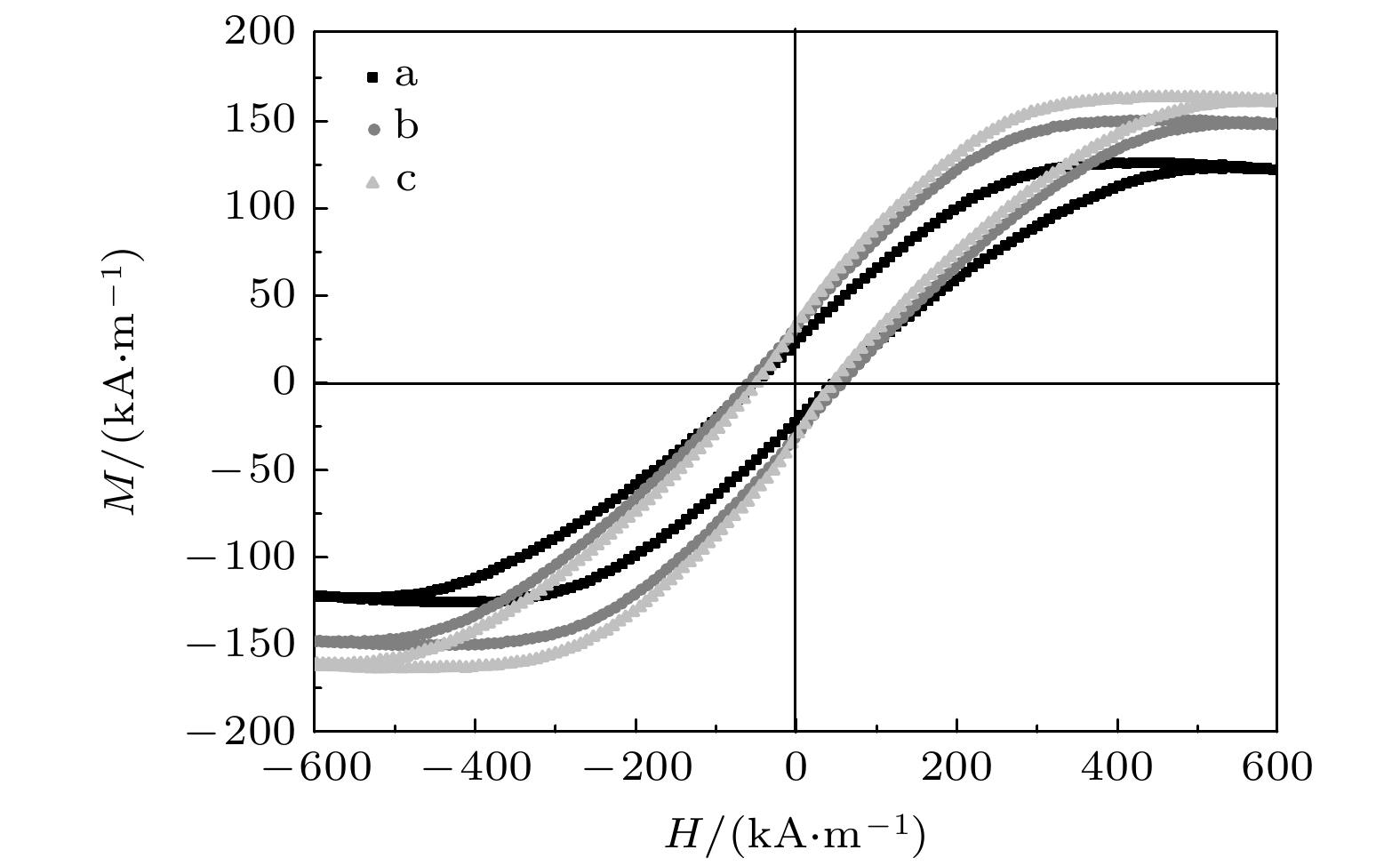
The multi-energy composite field micro-electrodeposition processing technology is used to prepare colorful structural coloration magnetic Al2O3-Co composite films each with a gradual microstructure. Under the action of the deposition electric field and the deflection electric field perpendicular to it, the microstructure, optical properties and magnetic properties of the composite films show gradual characteristics along the direction of the deflection electric field. By establishing an equivalent model of the microstructure, the mechanism of the microstructure change of the composite film is theoretically analyzed. Through software simulation, the distribution of Co ion deposition current density along the direction of the deflection electric field is quantitatively analyzed. The simulation results are consistent with the theoretical and experimental results. Through this study, we find that the micro-electrodeposition processing technology with using multi-energy field composite can control the micro-domain structure of the composite film from a microscopic point of view, and achieve the fine control of the magnetic and optical properties of the film micro-domain.
[1] Domagalski J T, Xifre-Perez E, Tabrizi M A, Ferre-Borrull J, Marsal L F 2021 J. Colloid Interface Sci. 584 15
[2] 程自强, 石海泉, 余萍, 刘志敏 2018 物理学报 67 197302
 Google Scholar
Cheng Z Q, Shi H Q, Yu P, Liu Z M 2018 Acta Phys. Sin. 67 197302
 Google Scholar
[3] Zhang K X, Yao C B, Wen X, Li Q H, Sun W J 2018 RSC Adv. 46 8
[4] Nie M, Sun H, Gao Z D, Li Q, Xue Z H, Luo J, Liao J M 2020 Electrochem. Commun. 115 106719
 Google Scholar
[5] Gu J J, Yang S M, Dong M Y, Qi Y K 2017 J. Alloys Compd. 728 25
[6] Yang S M, Han W, Li H T, Qi Y K, Gu J J 2015 J. Electrochem. Soc. 162 E123
 Google Scholar
[7] 梁玲玲, 赵艳, 冯超 2020 物理学报 69 065201
 Google Scholar
Liang L L, Zhao Y, Feng C 2020 Acta Phys. Sin. 69 065201
 Google Scholar
[8] Yue Y, Coburn K, Reed B, Liang H 2018 J. Appl. Electrochem. 48 3
[9] Ali H O 2017 Int. J. Surf. Eng. Coat. 95 6
[10] Mahmoud A T, Josep F B, Lluis F M 2020 Microchim. Acta 187 230
 Google Scholar
[11] Sergey E, Kushnir, Kirill S, Napolskii 2018 Mater. Des. 144 15
[12] Pankaj K, Josep F B, Lluis F M 2020 Adv. Mater. Interfaces 7 22
[13] Kirill S N, Alexey A N, Sergey E K 2020 Opt. Mater. 109 110317
 Google Scholar
[14] Mahmoud A T, Josep F B, Lluis F M 2020 Sci. Rep. 10 2356
 Google Scholar
[15] Mo R J, He L, Yan X M, Su T T, Zhou C X, Wang Z, Hong P Z 2018 Electrochem. Commun. 95 9
 Google Scholar
[16] Liudmyla R, Kateryna K, Volodymyr O, Menglei C 2021 Ukr. Chem. Journ. 86 5
[17] Li X C, Zhang T C, Gao P C 2018 Langmuir 34 49
[18] Liu S X, Tian J L, Zhang W 2021 Nanotechnology 32 222001
 Google Scholar
[19] Kapoor S, Ahmad H, Julien C M, Islam S S 2020 Appl. Surf. Sci. 512 145654
 Google Scholar
[20] Sistani M, Staudinger P, Greil J, Holzbauer M, Detz H, Bertagnolli E, Lugstein A 2017 Nano Lett. 17 8
 Google Scholar
[21] Fang J, Chen S, Vandenberghe W G, Fischetti M V 2017 IEEE Trans. Electron Devices 64 2758
 Google Scholar
[22] 杨淑敏, 韩伟, 顾建军, 李海涛, 岂云开 2015 物理学报 64 076102
 Google Scholar
Yang S M, Han W, Gu J J, Li H T, Qi Y K 2015 Acta Phys. Sin. 64 076102
 Google Scholar
[23] Ruiz-Clavijo A, Caballero-Calero O, Martín-González M 2021 Nanoscale 13 4
-
图 2 氧化铝薄膜和Al2O3-Co复合薄膜数码照片及XRD图谱 (a) 氧化电压20 V, 氧化时间11 min条件下制备的氧化铝薄膜数码照片; (b) 沉积电压12 V, 沉积时间60 s, 偏转电场120 V/m条件下制备的Al2O3-Co复合薄膜数码照片; (c) 图2(b) 所示薄膜的XRD图谱
Figure 2. Digital photos of alumina film and Al2O3-Co composite film and XRD diffraction pattern: (a) Digital photo of alumina film oxidized with a voltage of 20 V for 11 min; (b) digital photo of Al2O3-Co composite film deposited with a voltage of 12 V for 60 s and deflection field of 120 V/m; (c) XRD diffraction pattern of Al2O3-Co composite film shown in Fig. 2(b).
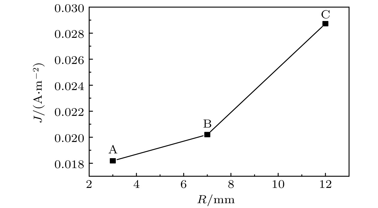
图 6 Al2O3-Co复合薄膜沿径向电流密度分布曲线
Figure 6. The curve of deposition current density along the radial of Al2O3-Co composite film shown in Fig.2 (b).
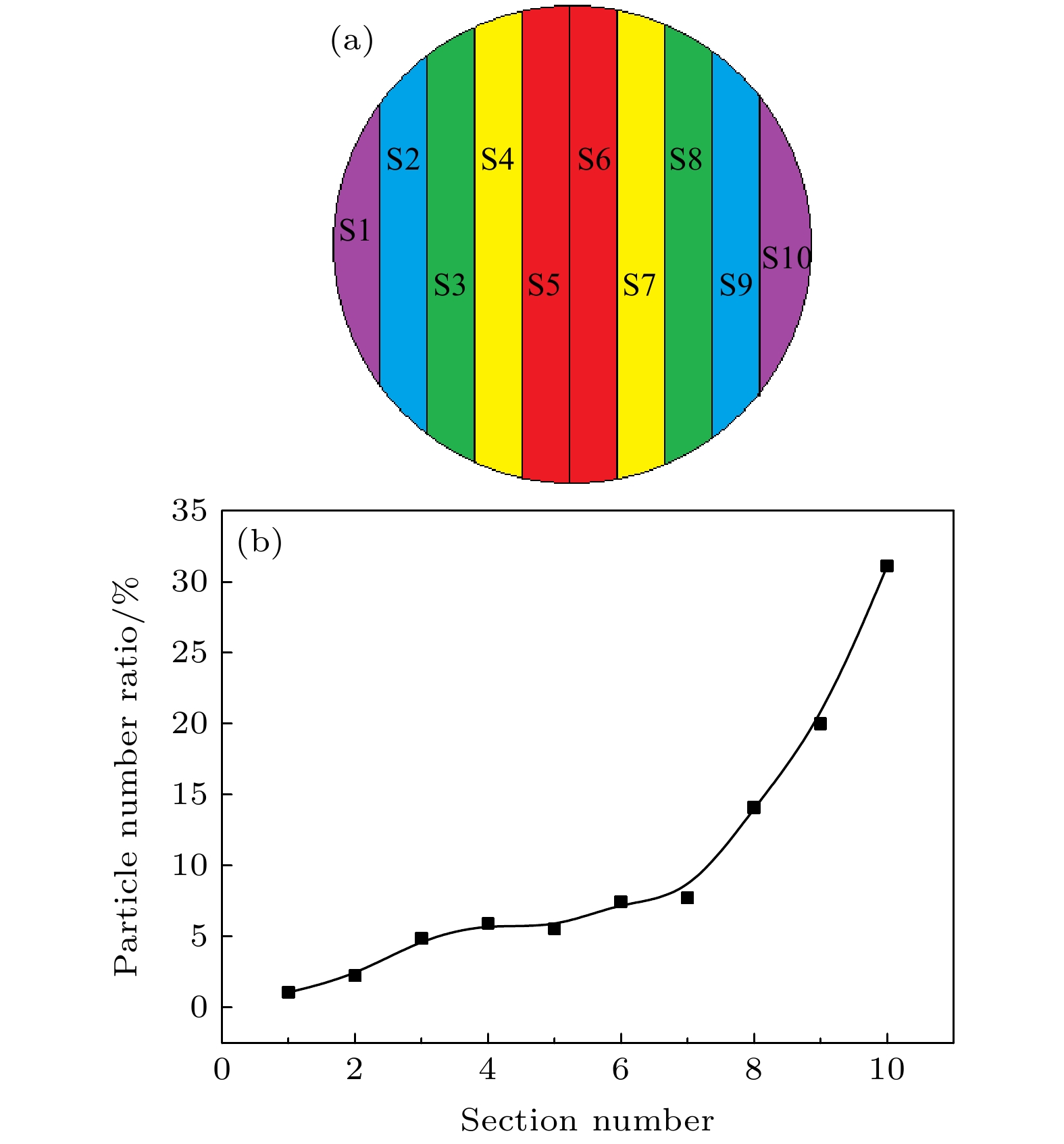
图 7 Al2O3-Co复合薄膜区域划分示意图和单位面积沉积率曲线 (a) Al2O3-Co复合薄膜沿径向不同区域划分示意图; (b) 不同划分区域单位面积沉积率曲线
Figure 7. Partition diagram and curve of per unit area deposition rate of Al2O3-Co composite film: (a) Diagram of different regions along the radial direction of Al2O3-Co composite film shown in Fig.2 (b); (b) the curve of deposition rate per unit area via divided regions.
图 10 Al2O3-Co复合薄膜数码照片 (a) 氧化电压20 V氧化时间14 min, 沉积电压12 V, 偏转电场120 V/m, 沉积时间分别为30, 40, 50, 60 s; (b) 氧化电压20 V氧化时间分别为12, 13, 14和15 min, 沉积电压12 V, 沉积时间为60 s, 偏转电场120 V/m
Figure 10. Digital photos of Al2O3-Co composite films: (a) The films were oxidized with a voltage of 20 V for 14 min. Then they were deposited with a voltage of 12 V for 30, 40, 50, 60 s and deflection field of 120 V/m; (b) the films were oxidized with a voltage of 20 V for 12, 13, 14 and 15 min. Then they were deposited with a voltage of 12 V for 60 s and deflection field of 120 V/m.
图 11 Al2O3-Co复合薄膜数码照片 (a) 氧化电压20 V氧化时间14 min, 沉积电压为11, 12, 13 V, 沉积时间为60 s, 偏转电场120 V/m; (b) 氧化电压20 V氧化时间为14 min, 沉积电压12 V, 沉积时间为60 s, 偏转电场分别为100, 120 and 140 V/m
Figure 11. Digital photos of Al2O3-Co composite films: (a) The films were oxidized with a voltage of 20 V for 14 min. Then they were deposited with voltage 11, 12, 13 V for 60 s and deflection field of 120 V/m; (b) the films were oxidized with a voltage of 20 V for 14 min. Then they were deposited with a voltage 12 V for 60 s and deflection field of 100, 120 and 140 V/m.
区域 A B C 氧化铝模板厚度/nm 290 290 290 氧化铝-Co复合薄膜厚度/nm 305 295 290 结构
模型Co层厚度/nm 15 5 0 Co纳米线密度/(%) 30 60 100 孔洞底部Co纳
米线长度/nm160 160 160 孔洞顶部Co纳
米线长度/nm25 15 0 等效
结构
模型Co层等效厚度/nm 14 5 0 Co纳米线长度/nm 66 102 160 未填充纳米
孔洞长度/nm225 188 130 干涉级别 2 1 1 反射波长/nm 392 632 629 对应颜色 红紫色 橙黄色 橙红色 平均折射率 n(air-Al2O3)=1.55
n(Co)=2.09
n(Co-Al2O3)=1.69表 2 复合薄膜区域划分面积和20 us末各区域粒子数统计表
Table 2. Partition areas of the film and particle statistics at the end of 20 μs.
区域 S1 S2 S3 S4 S5 S6 S7 S8 S9 S10 面积/mm2 6.3 11.1 13.5 14.8 15.5 15.5 14.8 13.5 11.1 6.3 粒子数/个 3 11 29 39 38 53 49 84 98 87 -
[1] Domagalski J T, Xifre-Perez E, Tabrizi M A, Ferre-Borrull J, Marsal L F 2021 J. Colloid Interface Sci. 584 15
[2] 程自强, 石海泉, 余萍, 刘志敏 2018 物理学报 67 197302
 Google Scholar
Cheng Z Q, Shi H Q, Yu P, Liu Z M 2018 Acta Phys. Sin. 67 197302
 Google Scholar
[3] Zhang K X, Yao C B, Wen X, Li Q H, Sun W J 2018 RSC Adv. 46 8
[4] Nie M, Sun H, Gao Z D, Li Q, Xue Z H, Luo J, Liao J M 2020 Electrochem. Commun. 115 106719
 Google Scholar
[5] Gu J J, Yang S M, Dong M Y, Qi Y K 2017 J. Alloys Compd. 728 25
[6] Yang S M, Han W, Li H T, Qi Y K, Gu J J 2015 J. Electrochem. Soc. 162 E123
 Google Scholar
[7] 梁玲玲, 赵艳, 冯超 2020 物理学报 69 065201
 Google Scholar
Liang L L, Zhao Y, Feng C 2020 Acta Phys. Sin. 69 065201
 Google Scholar
[8] Yue Y, Coburn K, Reed B, Liang H 2018 J. Appl. Electrochem. 48 3
[9] Ali H O 2017 Int. J. Surf. Eng. Coat. 95 6
[10] Mahmoud A T, Josep F B, Lluis F M 2020 Microchim. Acta 187 230
 Google Scholar
[11] Sergey E, Kushnir, Kirill S, Napolskii 2018 Mater. Des. 144 15
[12] Pankaj K, Josep F B, Lluis F M 2020 Adv. Mater. Interfaces 7 22
[13] Kirill S N, Alexey A N, Sergey E K 2020 Opt. Mater. 109 110317
 Google Scholar
[14] Mahmoud A T, Josep F B, Lluis F M 2020 Sci. Rep. 10 2356
 Google Scholar
[15] Mo R J, He L, Yan X M, Su T T, Zhou C X, Wang Z, Hong P Z 2018 Electrochem. Commun. 95 9
 Google Scholar
[16] Liudmyla R, Kateryna K, Volodymyr O, Menglei C 2021 Ukr. Chem. Journ. 86 5
[17] Li X C, Zhang T C, Gao P C 2018 Langmuir 34 49
[18] Liu S X, Tian J L, Zhang W 2021 Nanotechnology 32 222001
 Google Scholar
[19] Kapoor S, Ahmad H, Julien C M, Islam S S 2020 Appl. Surf. Sci. 512 145654
 Google Scholar
[20] Sistani M, Staudinger P, Greil J, Holzbauer M, Detz H, Bertagnolli E, Lugstein A 2017 Nano Lett. 17 8
 Google Scholar
[21] Fang J, Chen S, Vandenberghe W G, Fischetti M V 2017 IEEE Trans. Electron Devices 64 2758
 Google Scholar
[22] 杨淑敏, 韩伟, 顾建军, 李海涛, 岂云开 2015 物理学报 64 076102
 Google Scholar
Yang S M, Han W, Gu J J, Li H T, Qi Y K 2015 Acta Phys. Sin. 64 076102
 Google Scholar
[23] Ruiz-Clavijo A, Caballero-Calero O, Martín-González M 2021 Nanoscale 13 4
Catalog
Metrics
- Abstract views: 7252
- PDF Downloads: 72
- Cited By: 0


 DownLoad:

