


-
The parasitic effect inside metal oxide field effect transistor regarded as the basic structure of large scale digital circuits, has long been considered as an important factor affecting the disturbance, upset and latchup of integrated circuits in pulsed γ-ray radiation environment. To investigate the turn-on mechanism of vertical parasitic effect in NMOSFET induced by pulsed γ-ray radiation, the 40 nm, 90 nm and 180 nm NMOSFET device models are constructed by TCAD and the normal electrical characteristics are calibrated. The trend of vertical parasitic triode current gain, the turn-on conditions of vertical parasitic triode and their influence on working state of NMOSFET are obtained. The simulation results are shown below. 1) The disturbance of well potential inside NMOSFET induced by pulsed γ-ray radiation is the main reason for the turn-on of vertical parasitic triode. 2) When vertical parasitic triode is turn-on, the large secondary photocurrent will be generated inside NMOSFET which will affect the working state of the transistor. 3) The current gain of vertical parasitic triode in NMOSFET decreases with the technology node decreasing. The results provide a theoretical basis for studying the transient ionizing radiation effects of electronic devices.
-
Keywords:
- transient ionizing radiation effect /
- parasitic effect /
- rise of well potential /
- secondary photocurrent
[1] Wirth J L, Rogers S C 1964 IEEE Trans. Nucl. Sci. 11 24
 Google Scholar
[2] Enlow E W, Alexander D R 1988 IEEE Trans. Nucl. Sci. 35 1467
Google Scholar
[3] Fjeldly T A, Deng Y Q, Shur M S, Hjalmarson H P, Muyshondt A, Ytterdal T 2001 IEEE Trans. Nucl. Sci. 48 1721
Google Scholar
[4] Alexander D R 2003 IEEE Trans. Nucl. Sci. 50 565
Google Scholar
[5] 赖祖武 1998 抗辐射电子学(北京: 国防工业出版社) 第288—300页
Lai Z W 1998 Radiation Electronics (Beijing: Defense Industry Press) pp288–300 (in Chinese)
[6] Lewis C 1995 Transient Radiation Effects on Electronics (Alexandria: Defense Nuclear Agency) pp200–245
[7] 马强, 林东生, 范如玉, 陈伟, 杨善潮, 龚建成, 王桂珍, 齐超 2010 原子能科学技术 44 545
Google Scholar
Ma Q, Lin D S, Fan R Y, Chen W, Yang S C, Gong J C, Wang G Z, Qi C 2010 Atomic Energy Science and Technology 44 545
Google Scholar
[8] Oh S C, Lee N H, Lee H H 2012 12th International Conference on Control, Automation and Systems Jeju Island, Korea, October 17–21, 2012 p1233
[9] 王桂珍, 林东生, 齐超, 白小燕, 杨善潮, 李瑞宾, 马强, 金晓明, 刘岩 2014 原子能科学技术 48 2165
Google Scholar
Wang G Z, Lin D S, Qi C, Bai X Y, Yang S C, Li R B, Ma Q, Jin X M, Liu Y 2014 Atomic Energy Science and Technology 48 2165
Google Scholar
[10] Massengill L W, Diehl-Nagle S E 1985 IEEE Trans. Nucl. Sci. 32 4026
Google Scholar
[11] Massengill L W, Diehl-Nagle S E 1986 IEEE Trans. Nucl. Sci. 33 1541
Google Scholar
[12] Li J L, Chen W, Li R B, Wang G Z, Yang S C 2019 3rd Internaltional Conference on Radiation Effects of Electronic Devices Chongqing, China, May 29–31, 2019 pp1–4
[13] Boselli G, Reddy V, Duvvury C 2005 43rd Annual International Reliability Physics Symposium San Jose, USA, April 17–21, 2005 p137
[14] Li R B, Chen W, Lin D S, Yang S C, Bai X Y, Wang G Z, Liu Y, Qi C, Ma Q 2012 Sci. Chin. Tech. Sci. 55 3242
Google Scholar
[15] Keshavarz A A, Fischer T A, Dawes W R, Hawkins C F 1988 IEEE Trans. Nucl. Sci. 35 1422
Google Scholar
[16] Olson B D, Amusan O A, Dasgupta S, Massengill L W, Witulski A F, Bhuva B L, Alles M L, Warrenm K M, Ball D R 2007 IEEE Trans. Nucl. Sci. 54 894
Google Scholar
[17] Ahlbin J R, Atkinson N M, Gadlage M J, Gaspard N J, Bhuva B L, Loveless T D, Zhang E X, Chen L, Massengill L W 2011 IEEE Trans. Nucl. Sci. 58 2585
Google Scholar
[18] 金晓明, 范如玉, 陈伟, 王桂珍, 林东生, 杨善潮, 白小燕 2010 原子能科学技术 44 1487
Google Scholar
Jin X M, Fan R Y, Chen W, Wang G Z, Lin D S, Yang S C, Bai X Y 2010 Atomic Energy Science and Technology 44 1487
Google Scholar
[19] Calienes W, Reis R, Anghel C, Vladimirescu A 2014 IEEE 57th International Midwest Symposium on Circuits and Systems Texas, USA, August 3–6, 2014 p655
[20] Wunsch T F, Hash G L, Hewlett F W, Treece R K 1991 IEEE Trans. Nucl. Sci. 38 1392
Google Scholar
[21] Dasgupta S 2007 M. S. Thesis (Nashville: Vanderbilt University)
[22] Atkinson N M 2010 M. S. Thesis (Nashville: Vanderbilt University)
[23] Li R B, Wang C H, He C H, Chen W, Li J L, Qi C, Liu Y 2020 Nucl. Instrum. Meth. B 470 32
Google Scholar
[24] Neamen D A 2007 Semiconductor Physics and Devices Basic Principles (Beijing: Publishing House of Electronics Industry) pp284–285
-
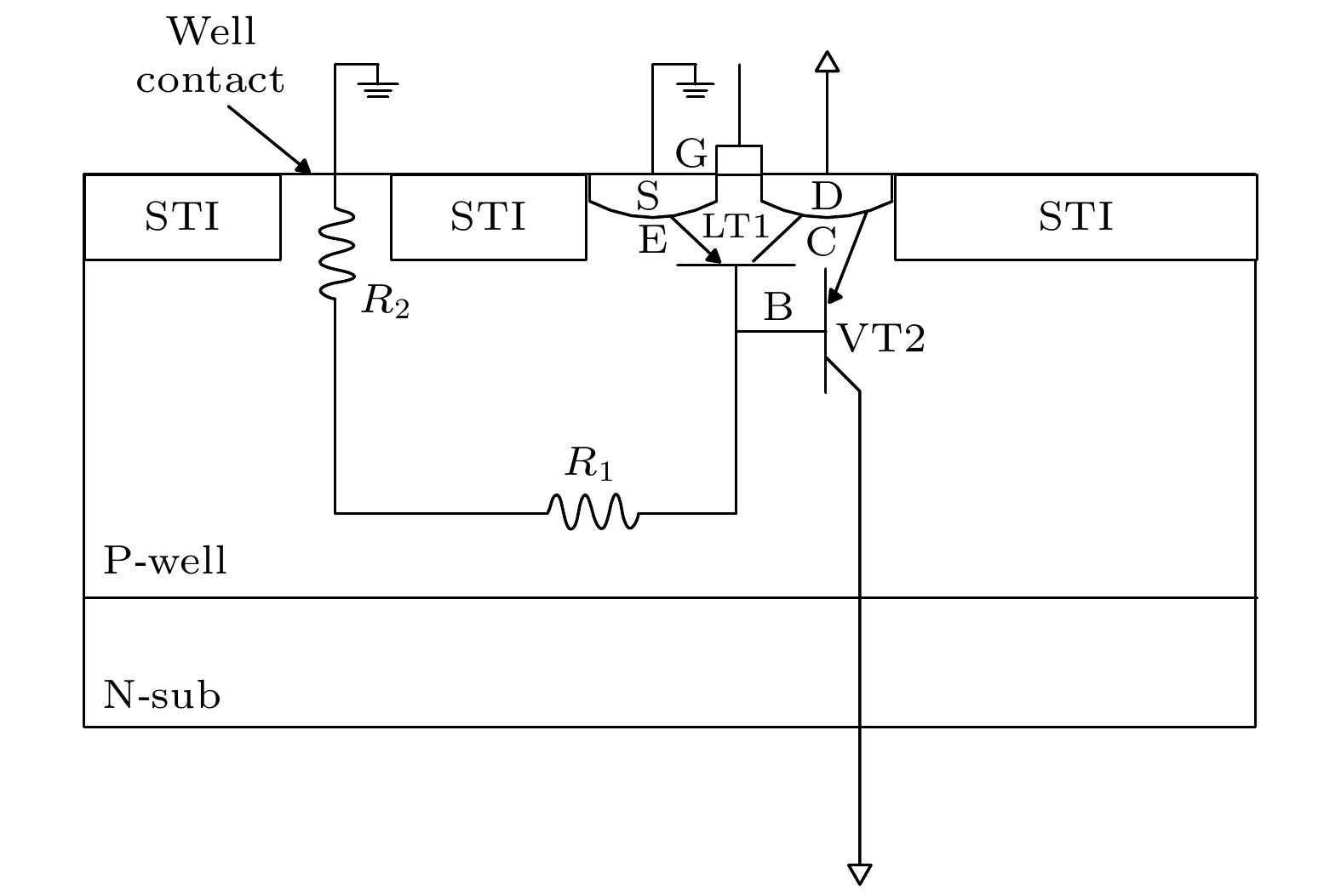
图 1 NMOS管寄生效应示意图
Figure 1. Parasitic effect schematic of NMOS.
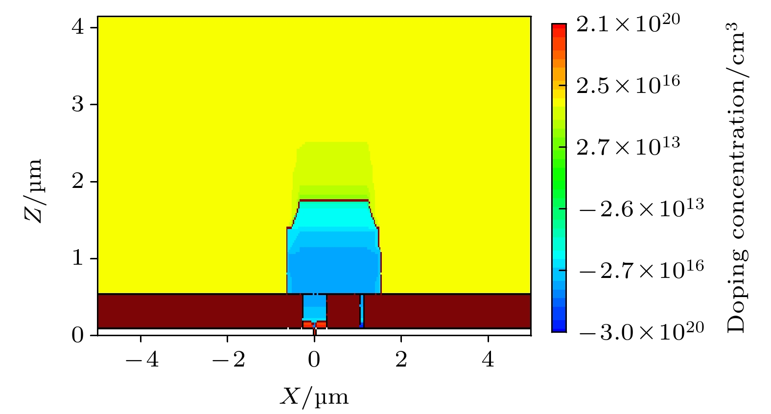
图 2 NMOS管二维剖面
Figure 2. Two-dimensional profile of NMOS.
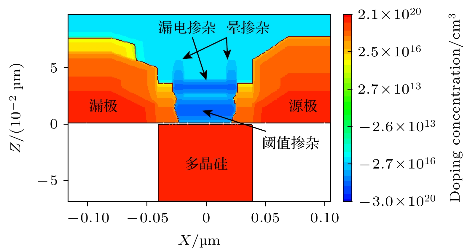
图 3 NMOS管沟道处掺杂
Figure 3. Channel doping of NMOS.
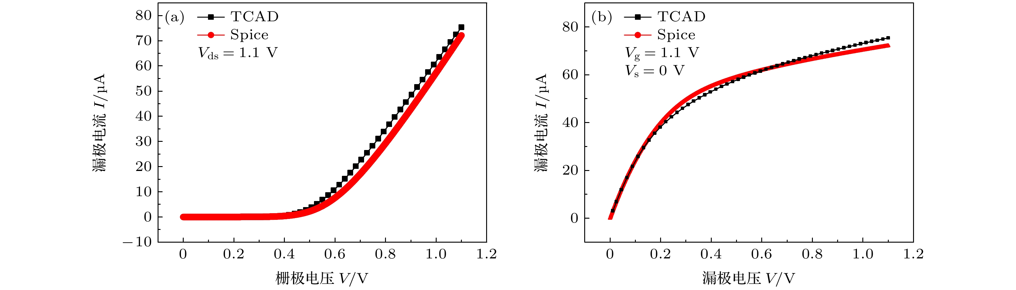
图 4 40 nm NMOS管常态特性校准曲线 (a) 转移特性曲线; (b) 输出特性曲线
Figure 4. Normal characteristic calibration curve of 40 nm NMOS: (a) Transfer characteristic curve; (b) output characteristic curve.

图 6 180 nm NMOS管常态特性校准曲线 (a) 转移特性曲线; (b) 输出特性曲线
Figure 6. Normal characteristic calibration curve of 180 nm NMOS: (a) Transfer characteristic curve; (b) output characteristic curve.
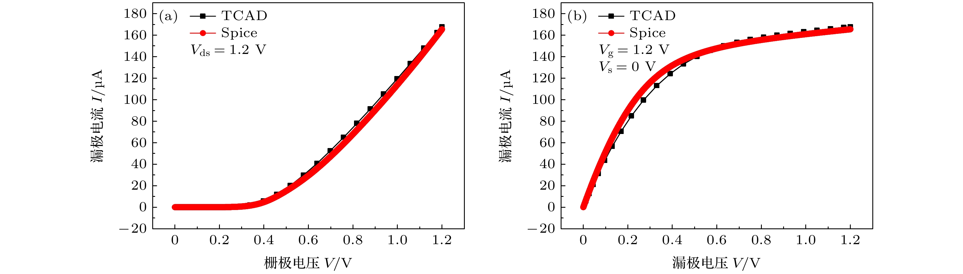
图 5 90 nm NMOS管常态特性校准曲线 (a)转移特性曲线; (b) 输出特性曲线
Figure 5. Normal characteristic calibration curve of 90 nm NMOS: (a) Transfer characteristic curve; (b) output characteristic curve.
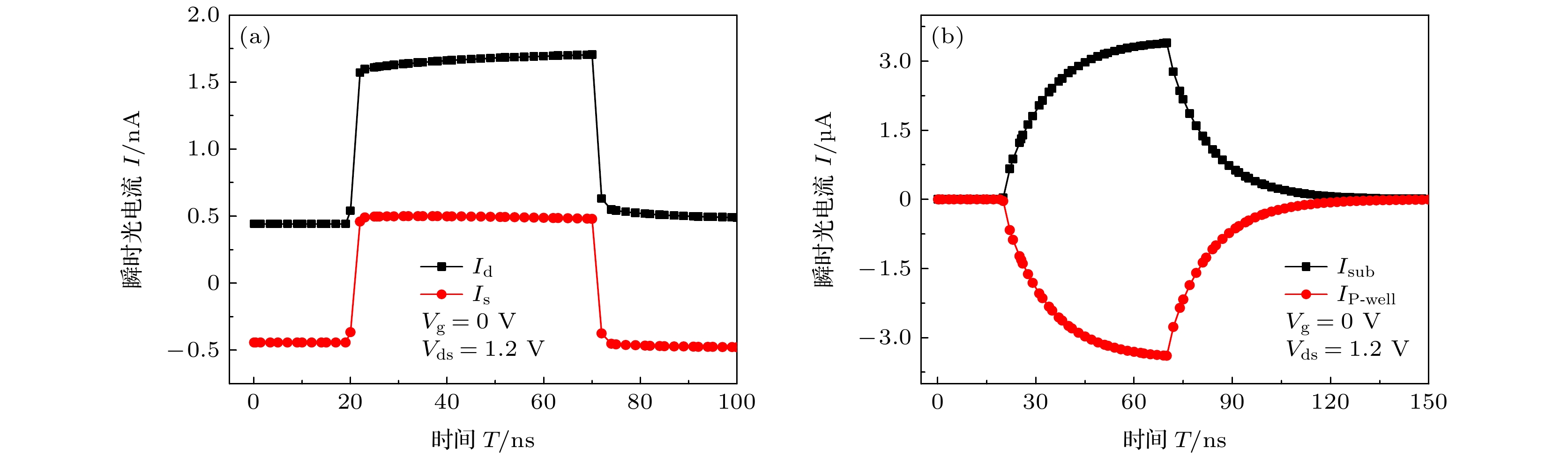
图 7 NMOS管截止时内部瞬时光电流 (a) 源极、漏极瞬时光电流; (b) P阱、衬底瞬时光电流
Figure 7. Photocurrent of NMOS when channel is cut-off: (a) Photocurrent of source and drain; (b) photocurrent of P-well and substrate.

图 8 NMOS管导通时内部光电流 (a) 源极、漏极瞬时光电流; (b) P阱、衬底瞬时光电流
Figure 8. Photocurrent of NMOS when channel is turn-on: (a) Photocurrent of source and drain; (b) photocurrent of P-well and substrate.
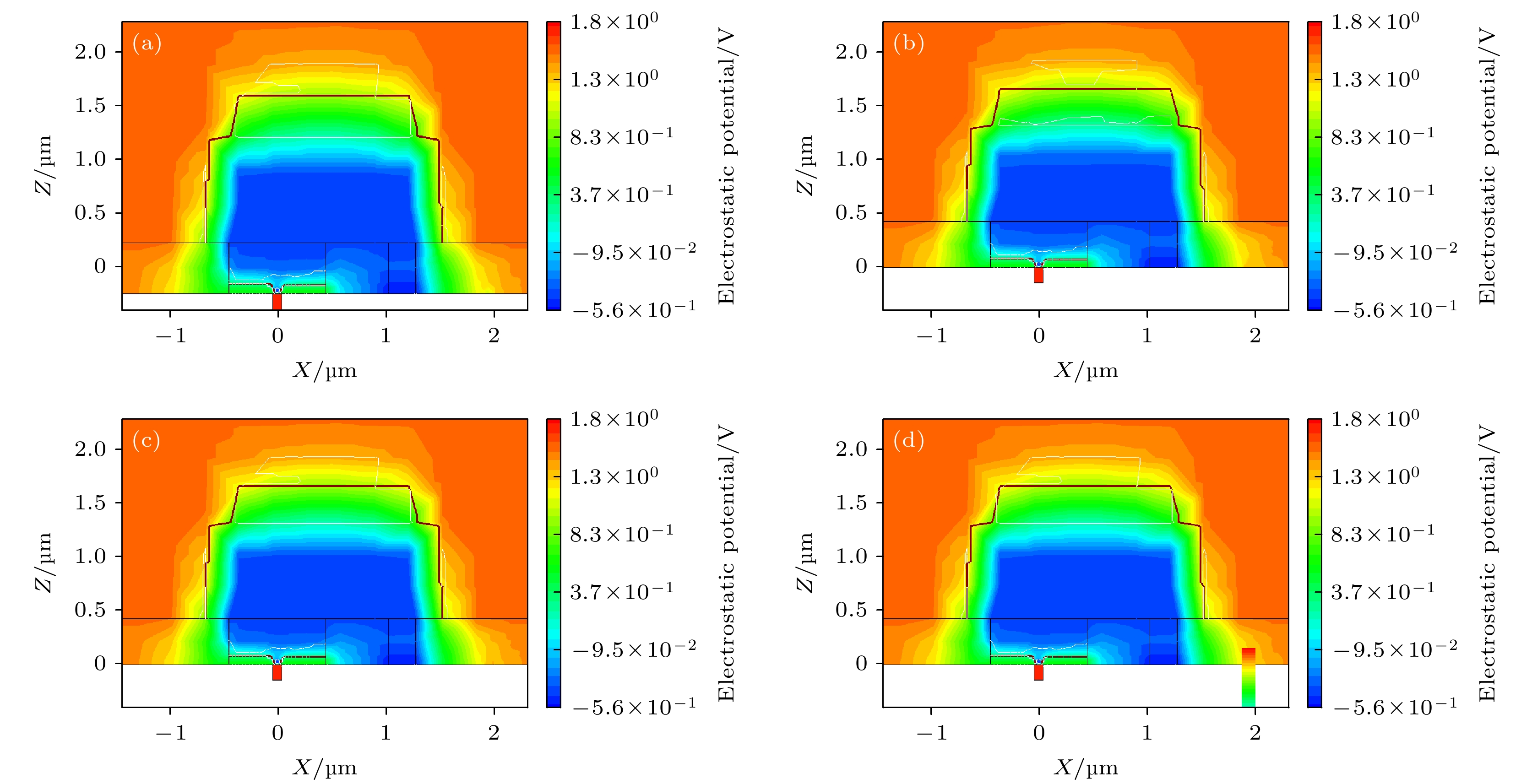
图 9 脉冲γ射线剂量率为2×10⁷Gy(Si)/s时NMOS管电势分布随时间变化 (a) 20 ns; (b) 70 ns; (c) 120 ns; (d) 200 ns
Figure 9. Variation of NMOS potential distribution over time when dose rate of transient γ-ray is 2×10⁷Gy(Si)/s: (a) 20 ns; (b) 70 ns; (c) 120 ns; (d) 200 ns.

图 10 脉冲γ射线剂量率为1×10¹⁰Gy(Si)/s时NMOS管电势分布随时间变化 (a) 20 ns; (b) 70 ns; (c) 120 ns; (d) 200 ns
Figure 10. Variation of NMOS potential distribution over time when dose rate of transient γ-ray is 1×10¹⁰Gy(Si)/s: (a) 20 ns; (b) 70 ns; (c) 120 ns; (d) 200 ns.
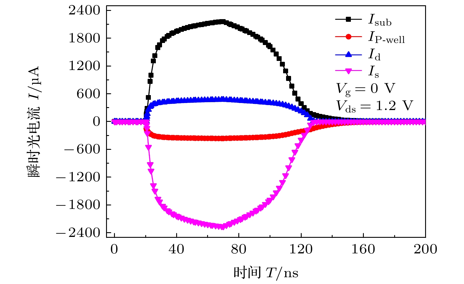
图 11 NMOS管截止时内部瞬时光电流
Figure 11. Photocurrent of NMOS when channel is cut-off.
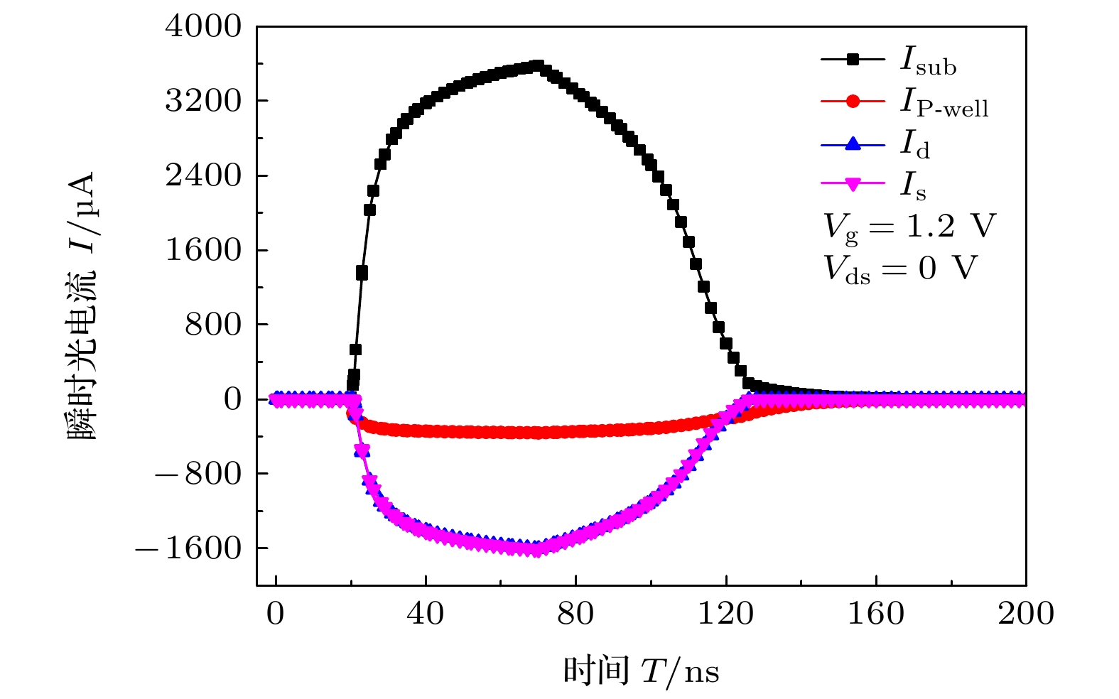
图 12 NMOS管导通时内部瞬时光电流
Figure 12. Photocurrent of NMOS when channel is turn-on.
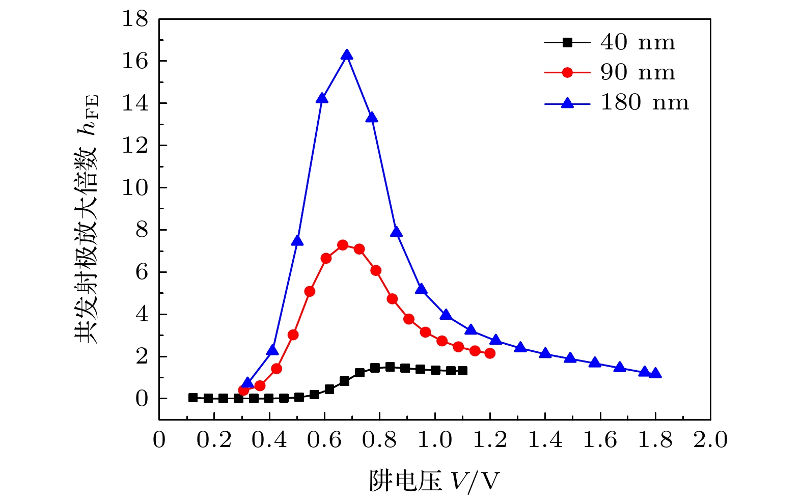
图 13 纵向寄生三极管电流增益
Figure 13. Gain of the vertial NPN triode vs voltage of pwell.

图 14 共发射极电流增益随集电极电流变化趋势
Figure 14. Tendency of current gain of the common emitter to the current of collector.
表 1 不同尺寸NMOS管结构参数与工艺参数
Table 1. Structure and process parameters of NMOS with different feature size.
工艺节点
λ/nm沟道长度
L/nm沟道宽度
W/nm源漏掺杂
/cm3晕掺杂
/cm3多晶硅掺杂
/cm3阈值掺杂
/cm3漏电掺杂
/cm340 40 120 2 × 10²⁰ 1.5 × 10¹⁹ 2 × 10²⁰ 7.5 × 10¹⁸ 7.5 × 10¹⁸ 90 80 200 2 × 10²⁰ 1 × 10¹⁸ 2 × 10²⁰ 8.2 × 10¹⁸ 8 × 10¹⁸ 180 180 540 1 × 10²⁰ 8 × 10¹⁷ 1 × 10²⁰ 8 × 10¹⁸ 7 × 10¹⁸  DownLoad: CSV
-
[1] Wirth J L, Rogers S C 1964 IEEE Trans. Nucl. Sci. 11 24
Google Scholar
[2] Enlow E W, Alexander D R 1988 IEEE Trans. Nucl. Sci. 35 1467
Google Scholar
[3] Fjeldly T A, Deng Y Q, Shur M S, Hjalmarson H P, Muyshondt A, Ytterdal T 2001 IEEE Trans. Nucl. Sci. 48 1721
Google Scholar
[4] Alexander D R 2003 IEEE Trans. Nucl. Sci. 50 565
Google Scholar
[5] 赖祖武 1998 抗辐射电子学(北京: 国防工业出版社) 第288—300页
Lai Z W 1998 Radiation Electronics (Beijing: Defense Industry Press) pp288–300 (in Chinese)
[6] Lewis C 1995 Transient Radiation Effects on Electronics (Alexandria: Defense Nuclear Agency) pp200–245
[7] 马强, 林东生, 范如玉, 陈伟, 杨善潮, 龚建成, 王桂珍, 齐超 2010 原子能科学技术 44 545
Google Scholar
Ma Q, Lin D S, Fan R Y, Chen W, Yang S C, Gong J C, Wang G Z, Qi C 2010 Atomic Energy Science and Technology 44 545
Google Scholar
[8] Oh S C, Lee N H, Lee H H 2012 12th International Conference on Control, Automation and Systems Jeju Island, Korea, October 17–21, 2012 p1233
[9] 王桂珍, 林东生, 齐超, 白小燕, 杨善潮, 李瑞宾, 马强, 金晓明, 刘岩 2014 原子能科学技术 48 2165
Google Scholar
Wang G Z, Lin D S, Qi C, Bai X Y, Yang S C, Li R B, Ma Q, Jin X M, Liu Y 2014 Atomic Energy Science and Technology 48 2165
Google Scholar
[10] Massengill L W, Diehl-Nagle S E 1985 IEEE Trans. Nucl. Sci. 32 4026
Google Scholar
[11] Massengill L W, Diehl-Nagle S E 1986 IEEE Trans. Nucl. Sci. 33 1541
Google Scholar
[12] Li J L, Chen W, Li R B, Wang G Z, Yang S C 2019 3rd Internaltional Conference on Radiation Effects of Electronic Devices Chongqing, China, May 29–31, 2019 pp1–4
[13] Boselli G, Reddy V, Duvvury C 2005 43rd Annual International Reliability Physics Symposium San Jose, USA, April 17–21, 2005 p137
[14] Li R B, Chen W, Lin D S, Yang S C, Bai X Y, Wang G Z, Liu Y, Qi C, Ma Q 2012 Sci. Chin. Tech. Sci. 55 3242
Google Scholar
[15] Keshavarz A A, Fischer T A, Dawes W R, Hawkins C F 1988 IEEE Trans. Nucl. Sci. 35 1422
Google Scholar
[16] Olson B D, Amusan O A, Dasgupta S, Massengill L W, Witulski A F, Bhuva B L, Alles M L, Warrenm K M, Ball D R 2007 IEEE Trans. Nucl. Sci. 54 894
Google Scholar
[17] Ahlbin J R, Atkinson N M, Gadlage M J, Gaspard N J, Bhuva B L, Loveless T D, Zhang E X, Chen L, Massengill L W 2011 IEEE Trans. Nucl. Sci. 58 2585
Google Scholar
[18] 金晓明, 范如玉, 陈伟, 王桂珍, 林东生, 杨善潮, 白小燕 2010 原子能科学技术 44 1487
Google Scholar
Jin X M, Fan R Y, Chen W, Wang G Z, Lin D S, Yang S C, Bai X Y 2010 Atomic Energy Science and Technology 44 1487
Google Scholar
[19] Calienes W, Reis R, Anghel C, Vladimirescu A 2014 IEEE 57th International Midwest Symposium on Circuits and Systems Texas, USA, August 3–6, 2014 p655
[20] Wunsch T F, Hash G L, Hewlett F W, Treece R K 1991 IEEE Trans. Nucl. Sci. 38 1392
Google Scholar
[21] Dasgupta S 2007 M. S. Thesis (Nashville: Vanderbilt University)
[22] Atkinson N M 2010 M. S. Thesis (Nashville: Vanderbilt University)
[23] Li R B, Wang C H, He C H, Chen W, Li J L, Qi C, Liu Y 2020 Nucl. Instrum. Meth. B 470 32
Google Scholar
[24] Neamen D A 2007 Semiconductor Physics and Devices Basic Principles (Beijing: Publishing House of Electronics Industry) pp284–285

 DownLoad:
Catalog
Metrics
- Abstract views: 5876
- PDF Downloads: 66
- Cited By: 0
