


-
Since British scientists Geim et al. (Novoselov K S, Geim A K, Morozov S V, Jiang D, Zhang Y, Dubonos S V, Grigorieva I V, Firsov A A
2004 Science 306 666 ) successfully peeded off single-layer graphene from multilayer graphite for the first time in 2004, two-dimensional materials have quickly caught the attention of scientists. Owing to its honeycomb structure, graphene exhibits many novel mechanical, thermal, electrical, and magnetic properties, which have attracted great attention and have broad application prospects in electronic devices and other fields. With the further development of research, more and more two-dimensional materials have been discovered successively, including silicene, germanene, and borylene. These two-dimensional materials have various excellent properties like graphene. Boron is one of the nearest-neighbor elements of carbon, it has proved to be able to form borophene, which has a lot of novel properties, including superconductivity and Dirac fermions. Several polymorphs of monolayer borophene have been synthesized on different metal surfaces, such as Au, Cu, Ag, Ir and Al. Using the nonequilibrium Green's function, we investigate the electronic transport properties of bilayer borophene which was synthesized recently. We first calculate the transmission spectra of different interlayer transition strengths when the electrode has two layers, then we calculate the currents of bilayer borophene under different voltages when the electrode has two layers, which both show bilayer borophene is metallic. With the enhancement of the interlayer transition strength, its conductivity first increases and then decays. We try to change the layer number of electrode. In scheme two, the left electrode is the lower half of the bilayer borophene while the right electrode is the upper half of the bilayer borophene. In scheme three both electrodes are the lower half of the bilayer borophene. In scheme four, both electrodes are the upper half of the bilayer borophene. In scheme five, the left electrode is the upper half of the bilayer borophene while the right electrode is the lower half of the bilayer borophene. We discover that the current decays greatly when the electrode is just one layer. For scheme three and scheme four, both left electrode and right electrode are the lower half of the bilayer borophene or the upper half of the bilayer borophene, the current will rise or decline in volatility. For scheme two or scheme five, the electrode is unsymmetrical, we find that the current will reach a maximum when interlayer transition increases. The reason for the above phenomenon is that the electrical conductivity of the upper half of the bilayer borophene is higher than that of the lower half, which causes the electrons of the lower half of the bilayer borophene to tunnel to the upper half so that the conductivity of bilayer borophene is enhanced when the interlayer transition strength is weak. However, when the interlayer transition strength is great, the frequent interlayer transition of electrons results in large scattering, thus causing its conductivity to decay. Finally, we consider the influence of the on-site disorder on the transport properties of the bilayer borophene, finding that its transport capability will be declined by increasing the disorder strength.-
Keywords:
- borophene nanoribbon /
- quantum transport /
- Green's function /
- current-voltage curve
[1] Novoselov K S, Geim A K, Morozov S V, Jiang D, Zhang Y, Dubonos S V, Grigorieva I V, Firsov A A 2004 Science 306 666
 Google Scholar
[2] 李亮亮, 孟凡伟, 邹鲲, 黄瑶, 彭倚天 2021 物理学报 70 086801
Google Scholar
Li L L, Meng F W, Zhou K, Huang Y, Peng Y T 2021 Acta Phys. Sin. 70 086801
Google Scholar
[3] 禹忠, 党忠, 柯熙政, 崔真 2016 物理学报 65 248103
Google Scholar
Yu Z, Dang Z, Ke X Z, Cui Z 2016 Acta Phys. Sin. 65 248103
Google Scholar
[4] Castro Neto A H, Guinea F, Peres N M R, Novoselov K S, Geim A K 2009 Rev. Mod. Phys. 81 109
Google Scholar
[5] Liu G, Lei X L, Wu M S, Xu B, Ouyang C Y 2014 J. Phys. Condens. Matter 26 355007
Google Scholar
[6] Liu G, Liu S B, Xu B, Ouyang C Y, Song H Y, Guan S, Yang S A 2015 J. Phys. Chem. Lett. 6 4936
Google Scholar
[7] Mannix A J, Zhou X F, Kiraly B, Wood J D, Alducin D, Myers B D, Liu X, Fisher B L, Santiago U, Guest J R, Yacaman M J, Ponce A, Oganov A R, Hersam M C, Guisinger N P 2015 Science 350 1513
Google Scholar
[8] Jackson K, Horoi M, Chaudhuri I, Frauenheim T, Shvartsburg A 2004 Phys. Rev. Lett. 93 013401
Google Scholar
[9] 秦志辉 2017 物理学报 66 216802
Google Scholar
Qin Z H 2017 Acta Phys. Sin. 66 216802
Google Scholar
[10] Zhai H-J, Kiran B, Li J, Wang L S 2003 Nat. Mater. 2 827
Google Scholar
[11] Tang H, Ismail-Beigi S 2007 Phys. Rev. Lett. 99 115501
Google Scholar
[12] Zhou X F, Dong X, Oganov A R, Zhu Q, Tian Y, Wang H T 2014 Phys. Rev. Lett. 112 085502
Google Scholar
[13] 李文辉, 陈岚, 吴克辉 2022 物理学报 71 108104
Li W H, Chen L, Wu K H 2022 Acta Phys. Sin. 71 108104
[14] Feng B, Zhang J, Zhong Q, Li W, Li S, Li H, Cheng P, Meng S, Chen L, Wu K 2016 Nat. Chem. 8 563
Google Scholar
[15] Li W, Kong L, Chen C, Gou J, Sheng S, Zhang W, Li H, Chen L, Cheng P, Wu K 2018 Sci. Bull. 63 282
Google Scholar
[16] Kiraly B, Liu X, Wang L, Zhang Z, Mannix A J, Fisher B L, Yakobson B I, Hersam M C, Guisinger N P 2019 ACS Nano 13 3816
Google Scholar
[17] Wu R, Drozdov I K, Eltinge S, Zahl P, Ismail-Beigi S, Božović I, Gozar A 2019 Nat. Nanotechnol. 14 44
Google Scholar
[18] Penev E S, Kutana A, Yakobson B I 2016 Nano Lett. 16 2522
Google Scholar
[19] Xiao R C, Shao D-F, Lu W, Lv H, Li J, Sun Y 2016 Appl. Phys. Lett. 109 122604
Google Scholar
[20] Feng B J, Sugino O, Liu R-Y, Zhang J, Yukawa R, Kawamura M, Iimori T, Kim H, Hasegawa Y, Li H, Chen L, Wu K, Kumigashira H, Komori F, Chiang T C, Meng S, Matsuda I 2017 Phys. Rev. Lett. 118 096401
Google Scholar
[21] Lian C, Hu S Q, Zhang J, Cheng C, Yuan Z, Gao S, Meng S 2020 Phys. Rev. Lett. 125 116802
Google Scholar
[22] Hu P J, Wang S X, Chen X F, Liang Z R, Fang T F, Guo A M, Xu H, Sun Q F 2022 npj Comput. Mater. 8 131
[23] Ohta T, Bostwick A, Seyller T, Horn K, Rotenberg E 2006 Science 313 951
Google Scholar
[24] Yankowitz M, Chen S, Polshyn H, Zhang Y, Watanabe K, Taniguchi T, Graf D, Young A F, Dean C R 2019 Science 363 1059
Google Scholar
[25] Chen C, Lv H, Zhang P, Zhuo Z, Wang Y, Ma C, Li W, Wang X, Feng B, Cheng P, Wu X, Wu K, Chen L 2022 Nat. Chem. 14 25
Google Scholar
[26] Liu X, Li Q, Ruan Q, Rahn M S, Yakobson B I, Hersam M C 2022 Nat. Mater. 21 35
Google Scholar
[27] Hu P J, Wang S X, Chen X F, Gao X H, Fang T F, Guo A M, Sun Q F 2022 Phys. Rev. Appl. 17 024074
[28] Sancho M P L, Sancho J M L, Rubio J 1984 J. Phys. F Met. Phys. 14 1205
Google Scholar
[29] Chen L, Ouyang F, Ma S, Fang T F, Guo A M, Sun Q F 2020 Phys. Rev. B 101 115417
Google Scholar
[30] Jiang Y, Hu L 2007 Phys. Rev. B 75 195343
Google Scholar
-
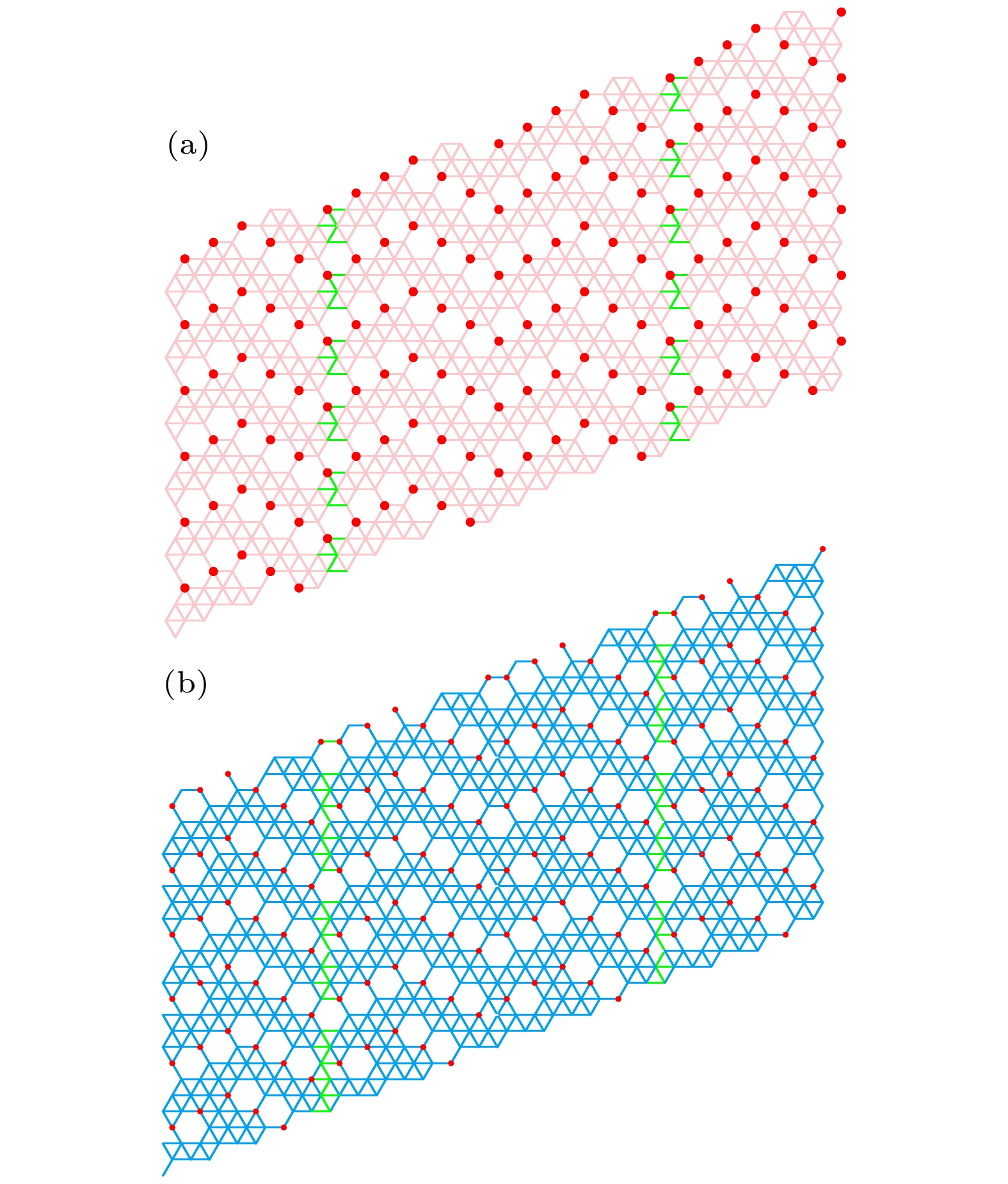
图 1 两端双层硼烯纳米带的结构 (a) 上层硼烯示意图; (b) 下层硼烯示意图; 上下两层硼烯通过红色标记的硼原子连接, 此时中心散射区长度包含2个晶胞, 而宽度包含1个晶胞
Figure 1. Structure of a two-terminal bilayer borophene nanoribbon. Schematics of the (a) top and (b) down layers. The boron atoms denoted by the red balls connect to their nearest neighbor ones at the other layer. Here, the size of the central scattering region contains two cells in length and one cell in width.

图 2 (a)双层硼烯纳米带的色散关系和(b)相应的电导, 此时左右电极均为半无限长的双层硼烯纳米带, 层间跃迁积分取为
$ {t}_{\rm{c}}=0.2 t $ Figure 2. (a) Dispersion relation of the bilayer borophene nanoribbon around the Fermi energy and (b) the corresponding transmission spectrum. Here, the left and right electrodes are the semi-infinite bilayer borophene nanoribbons and the interlayer hopping integral is set to
$ {t}_{\rm{c}}=0.2 t $ .
图 3 不同层间跃迁下, 双层硼烯纳米带的电导与入射电子能量的关系 (a)
$ {t}_{\rm{c}}=0 $ ; (b)$ {t}_{\rm{c}}=0.1 t $ ; (c)$ {t}_{\rm{c}}=0.2 t $ ; (d)$ {t}_{\rm{c}}=0.3 t $ ; (e)$ {t}_{\rm{c}}=0.9 t $ ; 此时左右电极均为半无限长的双层硼烯纳米带Figure 3. Energy-dependent conductance
$ G $ of the bilayer borophene nanoribbon connected to two semi-infinite bilayer ones by considering different interlayer hopping integrals: (a)$ {t}_{\rm{c}}=0 $ ; (b)$ {t}_{\rm{c}}=0.1 t $ ; (c)$ {t}_{\rm{c}}=0.2 t $ ; (d)$ {t}_{\rm{c}}=0.3 t $ ; (e)$ {t}_{\rm{c}}=0.9 t $ .
图 4 不同层间跃迁下, 双层硼烯纳米带的电流-电压曲线, 此时左右电极均为双层硼烯纳米带, 不同颜色曲线代表不同的层间跃迁积分
Figure 4. Current-voltage characteristics of the bilayer borophene nanoribbon connected to two semi-infinite bilayer ones by taking into account various interlayer hopping integrals.
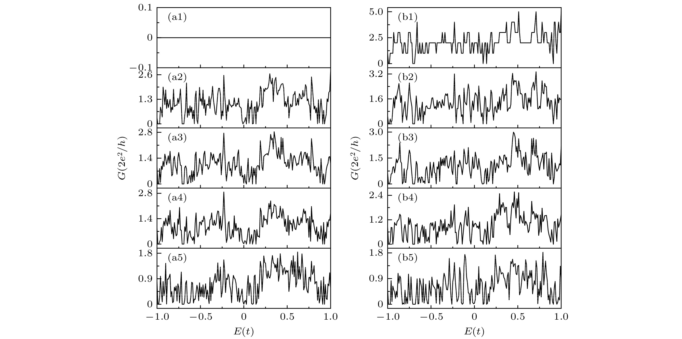
图 5 不同层间跃迁下, 方案二和方案三的电导与入射电子能量的关系 (a1)—(a5)方案二; (b1)—(b5)方案三; (a1) (b1)
$ {t}_{\rm{c}}=0 $ ; (a2) (b2)$ {t}_{\rm{c}}=0.1 t $ ; (a3) (b3)$ {t}_{\rm{c}}=0.2 t $ ; (a4) (b4)$ {t}_{\rm{c}}=0.3 t $ ; (a5) (b5)$ {t}_{\rm{c}}=0.9 t $ Figure 5. Energy-dependent conductance
$ G $ of the bilayer borophene nanoribbon by considering different contact and interlay hopping integrals: (a1)–(a5) Correspond to scheme 2 where the left electrode is the semi-infinite down layer in Fig. 2(b) and the right electrode is the semi-infinite up layer in Fig. 2(a); (b1)–(b5) refer to scheme 3 where both electrodes are the semi-infinite down layer in Fig. 2(b). (a1) (b1)$ {t}_{\rm{c}}=0 $ ; (a2) (b2)$ {t}_{\rm{c}}=0.1 t $ ; (a3) (b3)$ {t}_{\rm{c}}=0.2 t $ ; (a4) (b4)$ {t}_{\rm{c}}=0.3 t $ ; (a5) (b5)$ {t}_{\rm{c}}=0.9 t $ .
图 6 不同层间跃迁下, 四种方案的电流-电压曲线 (a)方案二; (b) 方案三; (c) 方案四; (d) 方案五; 图中不同颜色曲线代表不同的层间跃迁积分
Figure 6. Current-voltage characteristics of the bilayer borophene nanoribbon by considering different contact and interlay hopping integrals: (a) Scheme 2; (b) scheme 3; (c) scheme 4; (d) scheme 5. Here, scheme 4 corresponds to the case where both electrodes are the semi-infinite up layer, and scheme 5 to the case where the left electrode is the semi-infinite up layer and the right electrode is the semi-infinite down layer. Different curves in each panel denote various interlayer hopping integrals.
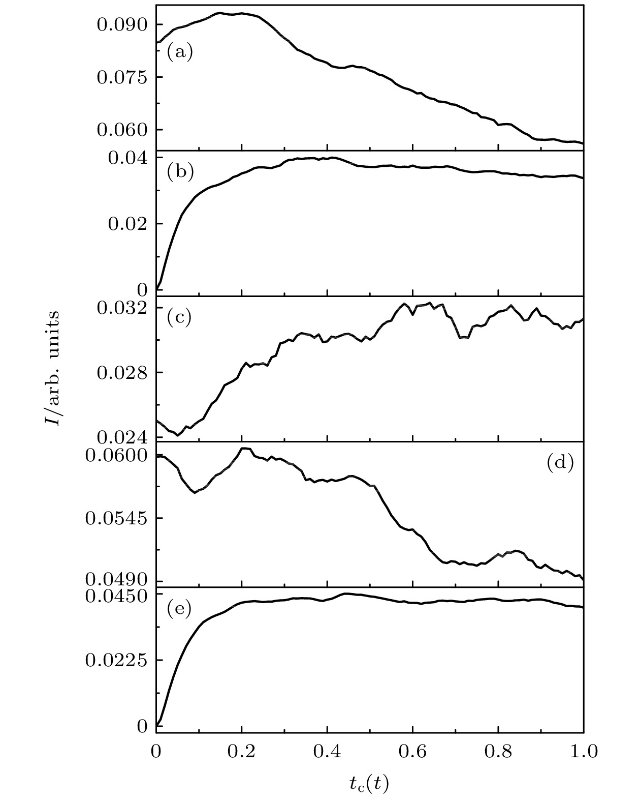
图 7 5种方案的电流与层间跃迁积分的关系 (a) 方案一; (b) 方案二; (c) 方案三; (d) 方案四; (e) 方案五; 此时左右电极的电压为
$ {V}_{\rm{S}\rm{D}}=1 $ Figure 7. Current at
$ {V}_{\rm{S}\rm{D}}=1 $ of the bilayer borophene nanoribbon by considering different contact, as a function of the interlayer hopping integral: (a) Scheme 1; (b) scheme 2; (c) scheme 3; (d) scheme 4; (e) scheme 5.
图 8 不同无序度下, 双层硼烯纳米带的电流-电压曲线. 此时左右电极均为双层硼烯纳米带, 层间跃迁积分为
$ {t}_{\rm{c}}=0.9 t $ , 不同颜色曲线代表不同的无序度Figure 8. Current-voltage characteristics of the bilayer borophene nanoribbon connected to two semi-infinite bilayer ones in the presence of on-site energy disorder with disorder strength
$ W $ . Here, the interlayer hopping integral is$ {t}_{\rm{c}}=0.9 t $ . -
[1] Novoselov K S, Geim A K, Morozov S V, Jiang D, Zhang Y, Dubonos S V, Grigorieva I V, Firsov A A 2004 Science 306 666
Google Scholar
[2] 李亮亮, 孟凡伟, 邹鲲, 黄瑶, 彭倚天 2021 物理学报 70 086801
Google Scholar
Li L L, Meng F W, Zhou K, Huang Y, Peng Y T 2021 Acta Phys. Sin. 70 086801
Google Scholar
[3] 禹忠, 党忠, 柯熙政, 崔真 2016 物理学报 65 248103
Google Scholar
Yu Z, Dang Z, Ke X Z, Cui Z 2016 Acta Phys. Sin. 65 248103
Google Scholar
[4] Castro Neto A H, Guinea F, Peres N M R, Novoselov K S, Geim A K 2009 Rev. Mod. Phys. 81 109
Google Scholar
[5] Liu G, Lei X L, Wu M S, Xu B, Ouyang C Y 2014 J. Phys. Condens. Matter 26 355007
Google Scholar
[6] Liu G, Liu S B, Xu B, Ouyang C Y, Song H Y, Guan S, Yang S A 2015 J. Phys. Chem. Lett. 6 4936
Google Scholar
[7] Mannix A J, Zhou X F, Kiraly B, Wood J D, Alducin D, Myers B D, Liu X, Fisher B L, Santiago U, Guest J R, Yacaman M J, Ponce A, Oganov A R, Hersam M C, Guisinger N P 2015 Science 350 1513
Google Scholar
[8] Jackson K, Horoi M, Chaudhuri I, Frauenheim T, Shvartsburg A 2004 Phys. Rev. Lett. 93 013401
Google Scholar
[9] 秦志辉 2017 物理学报 66 216802
Google Scholar
Qin Z H 2017 Acta Phys. Sin. 66 216802
Google Scholar
[10] Zhai H-J, Kiran B, Li J, Wang L S 2003 Nat. Mater. 2 827
Google Scholar
[11] Tang H, Ismail-Beigi S 2007 Phys. Rev. Lett. 99 115501
Google Scholar
[12] Zhou X F, Dong X, Oganov A R, Zhu Q, Tian Y, Wang H T 2014 Phys. Rev. Lett. 112 085502
Google Scholar
[13] 李文辉, 陈岚, 吴克辉 2022 物理学报 71 108104
Li W H, Chen L, Wu K H 2022 Acta Phys. Sin. 71 108104
[14] Feng B, Zhang J, Zhong Q, Li W, Li S, Li H, Cheng P, Meng S, Chen L, Wu K 2016 Nat. Chem. 8 563
Google Scholar
[15] Li W, Kong L, Chen C, Gou J, Sheng S, Zhang W, Li H, Chen L, Cheng P, Wu K 2018 Sci. Bull. 63 282
Google Scholar
[16] Kiraly B, Liu X, Wang L, Zhang Z, Mannix A J, Fisher B L, Yakobson B I, Hersam M C, Guisinger N P 2019 ACS Nano 13 3816
Google Scholar
[17] Wu R, Drozdov I K, Eltinge S, Zahl P, Ismail-Beigi S, Božović I, Gozar A 2019 Nat. Nanotechnol. 14 44
Google Scholar
[18] Penev E S, Kutana A, Yakobson B I 2016 Nano Lett. 16 2522
Google Scholar
[19] Xiao R C, Shao D-F, Lu W, Lv H, Li J, Sun Y 2016 Appl. Phys. Lett. 109 122604
Google Scholar
[20] Feng B J, Sugino O, Liu R-Y, Zhang J, Yukawa R, Kawamura M, Iimori T, Kim H, Hasegawa Y, Li H, Chen L, Wu K, Kumigashira H, Komori F, Chiang T C, Meng S, Matsuda I 2017 Phys. Rev. Lett. 118 096401
Google Scholar
[21] Lian C, Hu S Q, Zhang J, Cheng C, Yuan Z, Gao S, Meng S 2020 Phys. Rev. Lett. 125 116802
Google Scholar
[22] Hu P J, Wang S X, Chen X F, Liang Z R, Fang T F, Guo A M, Xu H, Sun Q F 2022 npj Comput. Mater. 8 131
[23] Ohta T, Bostwick A, Seyller T, Horn K, Rotenberg E 2006 Science 313 951
Google Scholar
[24] Yankowitz M, Chen S, Polshyn H, Zhang Y, Watanabe K, Taniguchi T, Graf D, Young A F, Dean C R 2019 Science 363 1059
Google Scholar
[25] Chen C, Lv H, Zhang P, Zhuo Z, Wang Y, Ma C, Li W, Wang X, Feng B, Cheng P, Wu X, Wu K, Chen L 2022 Nat. Chem. 14 25
Google Scholar
[26] Liu X, Li Q, Ruan Q, Rahn M S, Yakobson B I, Hersam M C 2022 Nat. Mater. 21 35
Google Scholar
[27] Hu P J, Wang S X, Chen X F, Gao X H, Fang T F, Guo A M, Sun Q F 2022 Phys. Rev. Appl. 17 024074
[28] Sancho M P L, Sancho J M L, Rubio J 1984 J. Phys. F Met. Phys. 14 1205
Google Scholar
[29] Chen L, Ouyang F, Ma S, Fang T F, Guo A M, Sun Q F 2020 Phys. Rev. B 101 115417
Google Scholar
[30] Jiang Y, Hu L 2007 Phys. Rev. B 75 195343
Google Scholar

 DownLoad:


Catalog
Metrics
- Abstract views: 7758
- PDF Downloads: 160
- Cited By: 0
