Loading [MathJax]/jax/element/mml/optable/SuppMathOperators.js

Search

Article

x

留言板

尊敬的读者、作者、审稿人, 关于本刊的投稿、审稿、编辑和出版的任何问题, 您可以本页添加留言。我们将尽快给您答复。谢谢您的支持!

姓名
邮箱
手机号码
标题
留言内容
验证码

Electromagnetic particle simulation of secondary electron multipactor characteristics in inner surface of 110 GHz microwave output window

Shu Pan-Pan Zhao Peng-Cheng Wang Rui

Shu Pan-Pan, Zhao Peng-Cheng, Wang Rui. Electromagnetic particle simulation of secondary electron multipactor characteristics in inner surface of 110 GHz microwave output window. Acta Phys. Sin., 2023, 72(9): 095202. doi: 10.7498/aps.72.20222235
Citation: Shu Pan-Pan, Zhao Peng-Cheng, Wang Rui. Electromagnetic particle simulation of secondary electron multipactor characteristics in inner surface of 110 GHz microwave output window. Acta Phys. Sin., 2023, 72(9): 095202. doi: 10.7498/aps.72.20222235

Electromagnetic particle simulation of secondary electron multipactor characteristics in inner surface of 110 GHz microwave output window

Shu Pan-Pan, Zhao Peng-Cheng, Wang Rui
Article Text (iFLYTEK Translation)
PDF
HTML
Get Citation
  • The secondary electron multipactor on the inner surface of the output window is one of the main factors limiting the power capacity of high power microwave. Therefore, it is of great significance to carry out relevant research. In this work, the process of secondary electron multipactor and the resulting loss of power are numerically simulated by using the electromagnetic particle model with one-dimensional spatial distribution and three-dimensional velocity distribution at the microwave frequency of 110 GHz. The influences of microwave electric field at the surface and dielectric material type on the power loss are studied. The simulation results show that the electron number density is higher than the critical cut-off number density after the secondary electron multipactor has reached the steady state, but the microwave electric field does not show obvious change. This is because the electrons in a very high electrostatic field are mainly concentrated in the domain of several micrometers near the dielectric surface, which is far less than the corresponding skin depth. The electron number density in the multipactor steady state increases with the microwave electric field increasing, but the ratio of the power loss to the microwave power at the surface increases slowly. After the multipactor reaches the steady state, the number density of electrons near the sapphire surface is the highest, followed by the number density near the crystal quartz surface, and the number density near the fused quartz surface is the lowest, so the corresponding power loss decreases successively. In order to verify the accuracy of the model, the simulated value of the multipactor threshold is compared with the experimental data, and the difference between them is discussed.
      Corresponding author: Zhao Peng-Cheng, pczhao@xidian.edu.cn
    • Funds: Project supported by the National Key Laboratory Foundation 2021-JCJQ-LB-006, China (Grant No. 6142411132116), the Natural Science Basic Research Program of Shaanxi Province, China (Grant Nos. 2023-JC-YB-512, 2023-JC-YB-042), the Fundamental Research Funds for the Central Universities, China (Grant No. ZYTS23075), and the China Postdoctoral Science Foundation (Grant No. 2019M653545)

    近年来, 高功率微波的峰值功率已发展到GW量级, 极易导致馈源介质窗真空侧发生次级电子倍增现象[1-4]. 次级电子倍增是真空中自由电子在强电磁场作用下与介质表面反复碰撞而使得电子数量急剧增长的现象. 在倍增过程中, 电子与介质表面之间的碰撞还会引起吸附在介质表面上的气体分子发生脱附[5]. 由于脱附气体分子的不断积累, 介质窗内侧环境逐渐由高真空向低气压转变. 在低气压中, 电子与气体分子之间发生雪崩式碰撞电离, 这对高功率微波传输产生很大的影响[6]. 因此, 介质表面次级电子倍增已成为限制微波功率容量提升的主要因素之一, 开展相关的研究具有重要的意义.

    国内外学者已对高功率微波介质表面次级电子倍增特性开展了大量的理论[7-12]和实验研究[13-21]. 在理论方面, Kishek和Lau[7]基于蒙特卡罗碰撞模型确定了次级电子产额为1时微波电场、频率和法向静电场之间的临界关系. Kim和Verboncoeur[8]采用静电粒子/蒙特卡罗碰撞方法研究了微波频率为2.85 GHz下真空和低气压介质表面击穿特性. 他们发现, 当介质表面的背景气压增加时, 击穿的主导机理由次级电子倍增逐渐转变为电子与中性粒子之间的碰撞电离. 蔡利兵和王建国[9]对1 GHz微波斜入射到介质表面时的次级电子倍增过程进行了静电粒子/蒙特卡罗碰撞模拟分析, 并比较了斜入射与正入射时的倍增参数(如平均电子能量)之间的差异. 在微波频率为11.42 GHz下, 李爽等[10]对包含刻槽结构的介质表面的电子碰撞能量进行了理论推导, 发现外加磁场并结合刻槽结构能够加强次级电子倍增的抑制效果. 左春彦等[11]通过静电粒子/蒙特卡罗碰撞模型描述高功率微波介质表面击穿过程, 重点分析了背景气体压强、微波电场振幅和频率对介质表面击穿特性的影响. Iqbal等[12]针对包含两个载频的微波介质表面击穿过程开展了蒙特卡罗碰撞模拟研究, 揭示了两个载频的相位和场强的差异对次级电子倍增的影响. 董烨等[13-15]分别采用粒子模型和流体模型对高功率微波窗沿面闪络过程进行了数值模拟研究, 获得了放电功率、沉积功率与入射微波功率的关系, 澄清了释气参数对输出窗击穿和微波传输的影响机制.

    在不同的外加磁场和介质表面结构下, 常超等[16-19]开展了X波段(8—12 GHz)次级电子倍增试验, 发现了若干有效抑制次级电子倍增的方法. 翁明等[20]通过加载介质的平行板结构对微波真空和低气压击穿特性进行了试验分析, 并测量了若干种材料的二次电子发射参数, 如最大次级电子产额以及对应的入射电子能量. Schaub等[21]测量了110 GHz微波作用下的次级电子倍增阈值, 发现其大约为传统微波(1—11 GHz)阈值的10倍. 他们还对蓝宝石、熔融石英和石英晶体等不同介质材料的倍增阈值进行了测量, 发现倍增阈值与材料种类密切相关.

    综上所述, 人们已对传统微波作用下的次级电子倍增特性开展了大量的理论分析, 然而很少研究涉及高频微波(如110 GHz)下的情况. 迄今, 我们仍旧对Schaub等[21]报道的实验结果缺乏足够的了解. 值得强调的是, 在他们的实验中, 如果介质表面附近的微波功率开始衰减, 则临界的微波电场被诊断为倍增阈值[21]. 然而, 由于之前的理论研究大多采用静电粒子模型, 以至于无法考虑次级电子倍增对微波功率的影响[8,9,11]. 本文采用一维空间分布和三维速度分布(1D3V)的电磁粒子模型对110 GHz微波次级电子倍增过程进行了模拟研究, 并考虑了次级电子倍增引起的损失功率, 这是本文与之前理论研究的主要区别. 重点研究了介质表面处的微波电场和材料种类对损失功率的影响, 旨在为相关的实验诊断提供一定的参考.

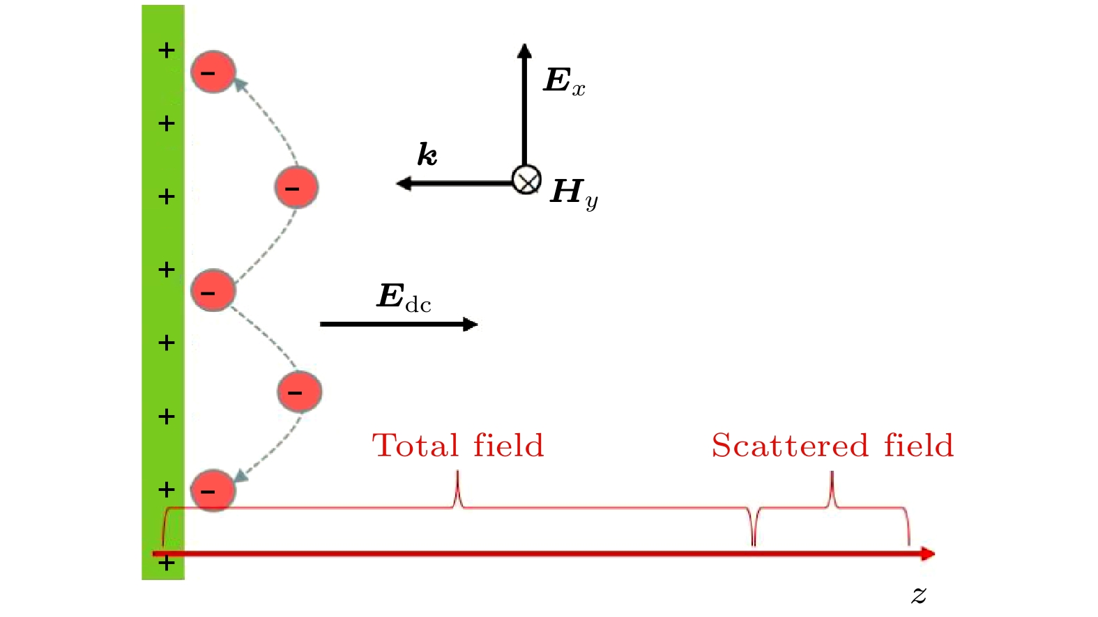
    在真空环境中, 令110 GHz均匀平面波沿负z方向入射到介质表面, 其电场分量平行于介质表面且沿x方向, 如图1所示. 在平面微波和法向静电场的共同作用下, 高能电子频繁往复地碰撞介质表面, 引发次级电子倍增效应. 在这种情况下, 可以用一维空间分布和三维速度分布(1D3V)的电磁粒子模型[6]研究介质表面附近的自由电子与微波之间的相互作用. 在该模型中, 用麦克斯韦方程组计算微波场, 并通过粒子算法描述电子运动及其与介质表面的碰撞反应[22]. 粒子算法与麦克斯韦方程组通过电流密度耦合在一起.

    图 1 高功率微波作用下介质表面次级电子倍增的示意图\r\nFig. 1. Schematic diagram of secondary electron multipactor on dielectric surface under high power microwave
    图 1  高功率微波作用下介质表面次级电子倍增的示意图
    Fig. 1.  Schematic diagram of secondary electron multipactor on dielectric surface under high power microwave

    由于本文考虑均匀平面波垂直入射到介质表面的情况, 所以采用一维麦克斯韦方程组计算微波场量的时空演变, 如图1所示. 在这种情况下, 微波电场沿x方向且平行于介质表面, 微波磁场的方向平行于y轴, 两者可表示为Emw=exExHmw=eyHy. 关于ExHy的麦克斯韦方程组可写为

    Ext=1ϵ0Hyz1ϵ0Jx, (1)
    Hyt=1μ0Exz, (2)

    其中, ϵ0μ0是真空的介电常数和磁导率. 介质表面附近存在大量的电子, 它们在微波场和法向静电场的作用下高速运动, 因而形成很强的电流. 在方程(1)中, Jx是该电流密度在x方向的分量.

    通过时域有限差分方法[23]求解方程(1)和方程(2), 得到时空演变的ExHy. 关于这两个方程的差分格式如下:

    En+1x(k)=Enx(k)Δtϵ0Δz×[Hn+1/2y(k+12)Hn+1/2y(k12)]Δtϵ0Jn+1/2x(k), (3)
    Hn+1/2y(k+12)=Hn1/2y(k+12)Δtμ0Δz×[Enx(k+1)Enx(k)], (4)

    其中Δt是时间步长, Δz是空间步长, 上标n=0,1,2,3,代表t=nΔt的时刻, k=0,1,2,3,代表z=kΔz的位置. 在计算域的边界上, 需要采取边界条件计算微波场量. 尽管Mur吸收边界的方程形式比较简单, 但是它在处理一维问题上是精确的. 因此, 本文采用Mur吸收边界条件计算边界上的微波电场. 如在左边界上(k=0), Mur吸收边界条件可以写为[23]

    En+1x(0)=Enx(1)+Scμrϵr1Scμrϵr+1[En+1x(1)Enx(0)], (5)

    其中, Sc=cΔt/Δz为稳定性条件, μrϵr分别为介质的相对磁导率和介电常数. 由于静电场的束缚作用, 次级电子倍增产生的电子主要分布在介质表面附近10 μm的区域. 为了分辨该数密度, 本文采取了很小的空间步长, 即Δz=0.15 μm. 根据稳定性条件, 时间步长取为Δt=Δz/c, 其中c为光速.

    为了便于计算电子对微波功率的反射和吸收, 将总场/散射场边界条件[23]引入上述的差分格式中. 设置总场与散射场之间的边界靠近计算域的右边界(见图1), 使得电子倍增发生在总场区. 在这种情况下, 计算空间被分割成总场区和散射场区, 而反射场可直接在散射场区获得. 通过计算反射场振幅Erm与入射场振幅Eim之比得到反射系数Γ. 在靠近计算域左边界的介质中, 确定传输电场的振幅Etm, 进而得到传输系数τ=Etm/Eim. 因此, 反射功率Pr、传输功率Pt以及吸收功率Pa与入射功率Pin的比值可写为

    Pr/Pin=Γ2, (6)
    Pt/Pin=ϵrτ2, (7)
    PaPin=1PrPinPtPin. (8)

    在次级电子倍增发生之前, 由于介质与真空的阻抗不匹配, 导致两者的分界面上存在明显的反射, 相应的反射功率比值记为Pr0/Pin. 在次级电子倍增达到稳态之后, 微波反射是由介质表面与电子共同造成的, 相应的反射功率比值记为Pr1/Pin. 因此, 电子对微波的反射功率与入射功率之比应该等于

    PrPin=Pr1PinPr0Pin, (9)

    由于介质表面附近的损失功率包括电子对微波功率的反射和吸收, 所以损失功率Ploss与入射功率之比为

    PlossPin=PrPin+PaPin, (10)

    值得注意的是, 次级电子倍增通常发生在介质表面附近的区域, 因而观察损失功率与介质表面处微波功率的比值更具有参考意义. 由图1可见, 介质表面位于波节的位置, 故其附近的微波电场振幅EsmEim(1+Γ0) (Γ0<0), 其中Γ0为次级电子倍增发生之前介质表面的反射系数. 在这种情况下, 由次级电子倍增引起的损失功率与介质表面处微波功率Ps之比可表示为

    PlossPs=1(1+Γ0)2PlossPin. (11)

    粒子算法是通过跟踪大量带电粒子的位置和速度等物理量, 再对它们进行统计平均, 进而得到宏观物理特性的数值方法[22]. 由于本文主要考虑真空环境次级电子倍增过程, 所以仅仅需要跟踪电子的运动情况. 在微波场和法向静电场的共同作用下, 电子的速度和位置满足如下方程:

    ddtmeυe=qe(Edc+Emw+μ0υe×Hmw), (12)
    dzdt=υz, (13)

    其中meqe分别为电子的质量和电量, υe是电子的速度, υzυez方向上的分量, Edc是由电子与介质表面上的正电荷共同产生的静电场, 其垂直于介质表面. Edc可通过一维泊松方程确定, 相关的方程如下:

    Edc=ϕzez, (14)
    2ϕz2=ρϵ0, (15)

    其中ϕ为电势, ρ为电荷密度. 通过求解方程(12)和方程(13)确定各个电子的速度和位置, 再对这些电子的速度和位置进行统计平均得到ρ和方程(1)中的Jx. 基于中心差分方法离散方程(15), 相应的差分格式构成了三对角矩阵. 利用传统的追赶法求解该矩阵, 得到ϕEdc.

    电子与介质表面之间的相互作用对次级电子倍增的发展至关重要. 当初级电子撞击介质表面时, 若次级电子产额大于1, 则导致电子数量急剧增加. 次级电子产额取决于初级电子的入射能量和入射角度以及表面材料. 根据Vaughan[24]报道的经验模型, 次级电子产额与入射电子能量和入射角度之间的关系如下:

    δ(εe,θ)=δmax0[1+θ2/(2π)]f(α), (16)
    α=εeεminεmax0εmin, (17)
    f(α)={[αe(1α)]0.56,α (18)

    其中 \varepsilon_\mathrm{e} θ是入射电子能量和入射角度, \delta_\mathrm{max0} 是电子垂直碰撞介质表面时的最大次级电子产额, \varepsilon_\mathrm{min}\approx12.5\;{\rm eV} 为次级电子产额大于零时的临界能量, \varepsilon_\mathrm{max0} 是对应于 \delta_{\mathrm{max0}} 的电子能量. 表1所列为3种介质材料的次级电子发射参数[21]和电磁参数. 在该表中, \epsilon_{\mathrm{r}} \mu_\mathrm{r} 分别为介质材料的相对介电常数和磁导率. 由于从介质表面发射的次级电子的能量很低, 所以它们的速度被取为平均动能为2 eV的麦克斯韦-玻尔兹曼分布[8,9,11]. 本文采用蒙特卡罗方法对次级电子发射的能量和角度进行抽样.

    表 1  介质材料的次级电子发射参数[21]和电磁参数
    Table 1.  Secondary electron emission parameters[21] and electromagnetic parameters of dielectric materials
    材料类型次级电子发射参数 电磁参数
    \delta_{\mathrm{max0}}\varepsilon_{\mathrm{max0}}/eV \epsilon_{\mathrm{r}}\mu_\mathrm{r}
    蓝宝石7.8650101.0
    熔融石英2.94203.61.0
    石英晶体3.84004.61.0
    下载: 导出CSV 
    | 显示表格

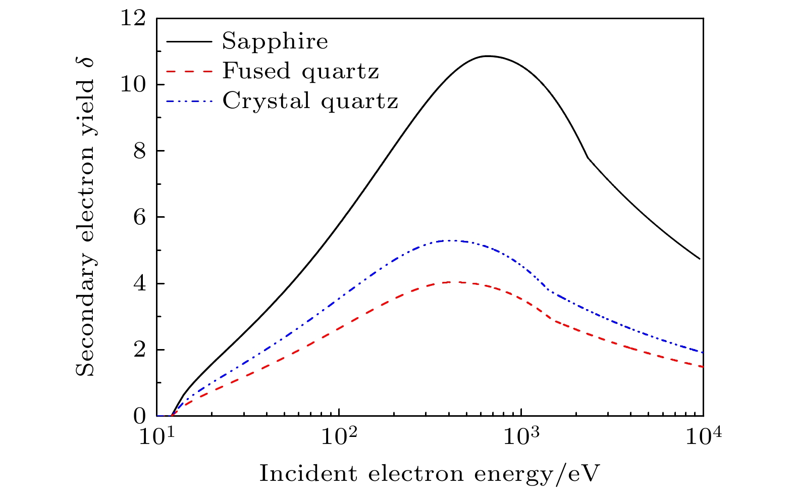
    在本文中, 入射的微波电场平行于介质表面, 导致电子撞击介质表面时的入射角度接近{\pi}/{2}. 因此, 我们观察了入射角为{\pi}/{2}下次级电子产额随入射电子能量的变化, 如图2所示. 在该图中, 介质材料分别取为蓝宝石、熔融石英和石英晶体. 当入射电子能量增加时, 次级电子产额先增加后减小. 在10 eV到30 eV之间, 这些曲线与次级电子产额为1的直线具有一个交叉点, 其被称为第一交叉点. 如果入射电子能量介于第一交叉点与104 eV之间, 则次级电子产额大于1. 在这种情况下, 发射的次级电子数量大于入射电子数量, 将引发次级电子倍增现象. 由图2还可以发现, 在相同的入射电子能量下, 蓝宝石的次级电子产额最高, 石英晶体的次之, 熔融石英的次级电子产额最低.

    图 2 在入射角等于${\pi}/{2}$以及介质材料分别为蓝宝石、熔融石英和石英晶体下, 次级电子产额δ随入射电子能量的变化\r\nFig. 2. Change of secondary electron yield δ with incident electron energy when the incident angle is ${\pi}/{2}$ and the dielectric materials are sapphire, fused quartz and crystal quartz respectively
    图 2  在入射角等于{\pi}/{2}以及介质材料分别为蓝宝石、熔融石英和石英晶体下, 次级电子产额δ随入射电子能量的变化
    Fig. 2.  Change of secondary electron yield δ with incident electron energy when the incident angle is {\pi}/{2} and the dielectric materials are sapphire, fused quartz and crystal quartz respectively

    以蓝宝石材料为例, 首先研究不同微波电场下次级电子倍增的时空演化特性, 重点考虑了由次级电子倍增引起的损失功率随微波电场的变化. 其中, 为验证模型及算法的准确性, 将损失功率的模拟值与实验数据进行了对比. 其次, 对不同介质材料下次级电子倍增的演化过程进行了模拟, 旨在揭示介质材料种类对损失功率的影响. 还比较了不同材料下次级电子倍增阈值的模拟值与实验数据, 并对两者的差异进行了解释.

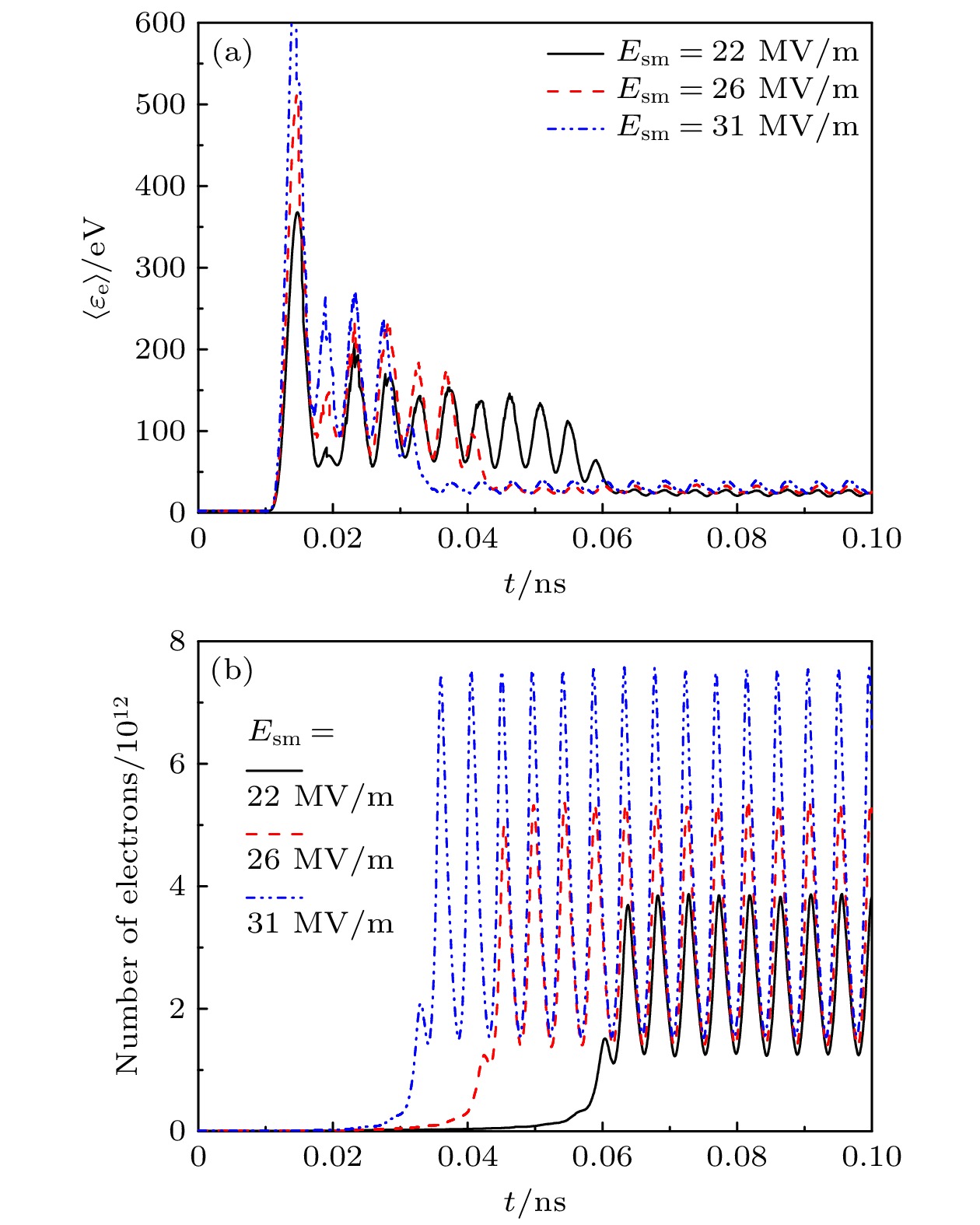
    图3所示为110 GHz微波作用下介质表面附近的平均电子能量和电子数量随时间的变化. 图中, 介质材料为蓝宝石, 介质表面附近的微波电场振幅 E_\mathrm{{sm}} 分别取为22, 26和31 MV/m. 注意 E_\mathrm{{sm}} 不同于入射电场振幅 E_\mathrm{{im}} , 两者满足如下关系: E_\mathrm{{sm}} = (1+\varGamma)E_\mathrm{{im}} . 在蓝宝石与真空的分界面上, 反射系数 \varGamma = -0.52 , 表明 E_\mathrm{{sm}} \approx 0.48 E_\mathrm{{im}} . 在 E_\mathrm{{sm}} = 22 MV/m下, 平均电子能量首先在100 eV周围振荡, 相应的次级电子产额明显大于1 (见图2), 导致电子数量显著增加. 随着时间的推移, 介质表面上的正电荷以及表面附近的电子越来越多, 由两者共同产生的法向静电场变得更高. 由于电子受到的静电力指向介质表面, 所以电子被微波电场加速的时间(渡越时间)随着法向静电场的增大而减小. 因此, E_\mathrm{{sm}} = 22 MV/m下平均电子能量在 0.05 ns之后逐渐降低, 直至稳定在次级电子产额为1的能量周围, 如图3(a)所示. 由图3(b)可见, 在次级电子倍增达到稳态之后, 电子数量的振荡周期是微波周期(0.0091 ns)的二分之一. 这是因为次级电子产额依赖于平均电子能量, 而平均电子能量则以微波频率的2倍振荡. 由图3还可发现, 随着介质表面附近微波电场的增加, 平均电子能量增加, 导致次级电子产额升高. 这使得电子倍增稳态所需要的时间减小以及电子数量变得更大.

    图 3 在介质材料为蓝宝石, 介质表面附近的微波电场振幅$E_\mathrm{{sm}}$取为不同值下, (a)平均电子能量$\langle\varepsilon_\mathrm{e}\rangle$和(b)电子数量随时间的变化\r\nFig. 3. Variation of (a) mean electron energy $\langle\varepsilon_\mathrm{e}\rangle$ and (b) number of electrons over time when the dielectric material is sapphire and the amplitude $E_\mathrm{{sm}}$ of microwave electric field near the dielectric surface takes different values
    图 3  在介质材料为蓝宝石, 介质表面附近的微波电场振幅E_\mathrm{{sm}}取为不同值下, (a)平均电子能量\langle\varepsilon_\mathrm{e}\rangle和(b)电子数量随时间的变化
    Fig. 3.  Variation of (a) mean electron energy \langle\varepsilon_\mathrm{e}\rangle and (b) number of electrons over time when the dielectric material is sapphire and the amplitude E_\mathrm{{sm}} of microwave electric field near the dielectric surface takes different values

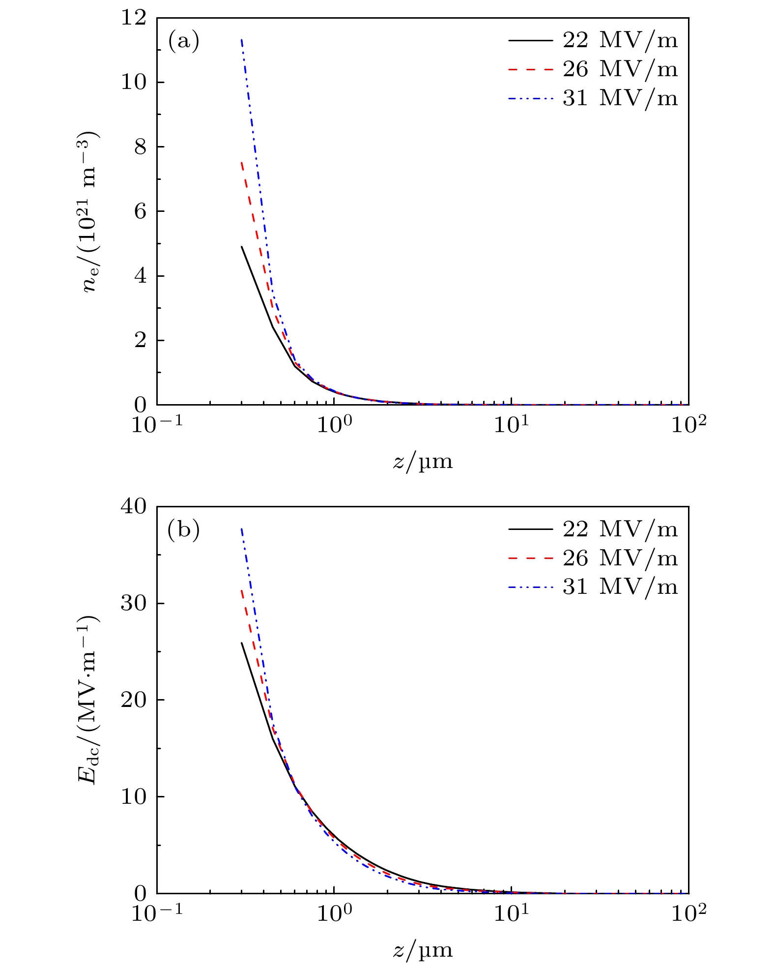
    在次级电子倍增达到稳态之后, 电子数密度 n_\mathrm{e} 和法向静电场 E_{\mathrm{dc}} 的空间分布如图4所示. 为了清晰地观察电子数密度和法向静电场随z的变化, 空间坐标取为对数坐标, 其中介质表面位于 z = 0.15 \;{\text{µ}}{\rm{m}} 的位置. 图4模拟条件与图3相同. 由图4(a)可见, 由于次级电子倍增的作用, 电子数密度在最靠近介质表面的位置具有一个峰值. 在介质表面附近存在很高的法向静电场(图4(b)), 电子受到指向介质表面的巨大作用力, 使得电子快速返回介质表面. 因此, 电子数密度随着z的增加而急剧降低. 当介质表面附近的微波电场振幅增加时, 电子数密度的峰值由5 \times 10^{21} m–3升高至1.1 \times 10^{22} m–3. 介质表面上正电荷的电量与空间中的电子电量等值异号, 并且介质表面处的静电场正比于正电荷的面密度. 因此, 静电场峰值随着微波电场振幅的增加而变得更高. 该静电场的峰值达到数十MV/m, 其与介质表面附近的微波电场振幅具有相同的量级. 随着远离介质表面, 空间中的电子将屏蔽介质表面上正电荷产生的静电场, 导致静电场随着z的增加而减小, 直至近似为零.

    图 4 在次级电子倍增达到稳态之后, (a)电子数密度$n_\mathrm{e}$和(b)法向静电场$E_{\mathrm{dc}}$随z的变化, 其中模拟条件与图3相同\r\nFig. 4. Spatial distributions of (a) electron number density $n_\mathrm{e}$ and (b) the normal electrostatic field $E_{\mathrm{dc}}$ after the secondary electron multipactor reaches the steady state, where the simulation conditions are the same as Fig. 3
    图 4  在次级电子倍增达到稳态之后, (a)电子数密度n_\mathrm{e}和(b)法向静电场E_{\mathrm{dc}}z的变化, 其中模拟条件与图3相同
    Fig. 4.  Spatial distributions of (a) electron number density n_\mathrm{e} and (b) the normal electrostatic field E_{\mathrm{dc}} after the secondary electron multipactor reaches the steady state, where the simulation conditions are the same as Fig. 3

    在传统微波(1—11 GHz)的作用下, 电子数密度峰值大约在1019 m–3的量级[8,11], 远低于图4所示的110 GHz微波下的情况, 具体原因如下所述. 在保持微波电场与频率之比不变的情况下, 产生的法向静电场与频率之比近似为一常数[7]. 换言之, 静电场随着微波频率的升高而增加. 再者, 介质表面处的静电场正比于介质表面上正电荷的数量. 由于整个放电系统具有电中性的特点, 正电荷的数量与空间中的电子数量相等. 因此, 微波频率越大, 电子数密度越高. 另外, 传统微波下电子数密度的分布宽度接近100 μm, 然而110 GHz微波下的分布宽度仅为若干μm. 这是因为传统微波下的静电场较低, 电子受到指向介质表面的作用力较小, 以至于电子能够漂移到距离介质表面更远的位置.

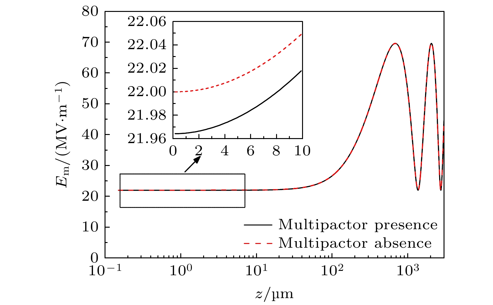
    在次级电子倍增发生之前, 介质与真空之间的分界面导致微波出现明显的反射, 进而在空间形成驻波, 如图5所示. 图中介质材料为蓝宝石, 表面处的电场振幅取为22 MV/m. 尽管微波电场振幅在空间是非均匀的, 但是次级电子倍增仅仅发生在介质表面附近, 即 z < 10 μm的区域(见图4(a)),因而相应的微波电场振幅可近似为均匀地分布. 在无碰撞的等离子体中, 存在临界截止数密度 n_{\mathrm{c}} = (\epsilon_0 m_{\mathrm{e}}/q_{\mathrm{e}}^2)\omega^2 , 其中ω为微波角频率[25]. 如果电子数密度超过 n_{\mathrm{c}} , 则微波不能在该媒质中传播. 当微波频率为110 GHz时, n_{\mathrm{c}}\approx1.5 \times 10^{20} m–3. 在次级电子倍增达到稳态之后, 电子数密度的峰值明显高于 n_{\mathrm{c}} (见图4(a)), 然而电子倍增达到稳态之后的微波电场振幅与没有发生倍增的情况之间具有很小的差异, 如图5所示. 当介质表面处的微波电场振幅取为其他值时, 也观察到了该现象. 为了解释倍增电子对微波传输的影响, 我们将电子等离子体类比为金属, 并引入了“趋肤深度”的概念. 当金属的厚度远大于趋肤深度时, 微波电场在其中的衰减很大, 但当金属的厚度小于趋肤深度时, 微波电场在其中的改变很小. 由于次级电子倍增产生的等离子体的厚度仅仅为10 μm左右(见图4(a)), 远小于等离子体的趋肤深度, 所以微波电场振幅的衰减很小. 我们也证实了若增大等离子体的厚度, 微波电场将发生更加明显的改变.

    图 5 电子倍增发生之前的微波电场振幅与电子倍增稳态之后的电场振幅之间的比较, 其中介质材料为蓝宝石, 表面处的电场振幅为22 MV/m\r\nFig. 5. Comparison of microwave electric field amplitude without electron multipactor with that after the secondary electron multipactor reaches the steady state. The dielectric material is sapphire, and the electric field amplitude at the surface is 22 MV/m
    图 5  电子倍增发生之前的微波电场振幅与电子倍增稳态之后的电场振幅之间的比较, 其中介质材料为蓝宝石, 表面处的电场振幅为22 MV/m
    Fig. 5.  Comparison of microwave electric field amplitude without electron multipactor with that after the secondary electron multipactor reaches the steady state. The dielectric material is sapphire, and the electric field amplitude at the surface is 22 MV/m

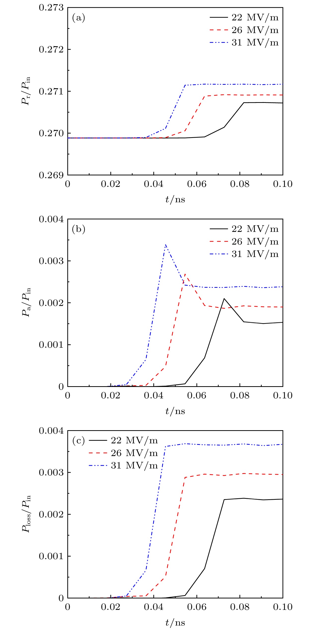
    图6所示为反射功率、吸收功率以及损失功率与入射功率的比值随时间的变化. 图中介质材料为蓝宝石, 介质表面处的微波电场振幅 E_\mathrm{{sm}} 分别取为22, 26和31 MV/m, 即模拟条件与图3相同. 由图6(a)可见, 在电子倍增的初期, 反射功率与入射功率之比 P_{\mathrm{r}}/P_{\mathrm{in}} 大约为0.2699. 这主要归因于介质与真空之间的分界面对微波的反射. 随着时间的推移, P_{\mathrm{r}}/P_{\mathrm{in}} 首先增加, 接着在电子倍增达到稳态后几乎保持不变. 电子倍增达到稳态后的反射功率与电子倍增初期的反射功率之间的差异是由于电子对微波的反射. 由此可推断, 电子对微波的反射功率与入射功率之比很小, 大约在0.001的量级上. 吸收功率随时间的变化趋势与反射功率的情况相似, 如图6(b)所示. 在次级电子倍增达到稳态之后, 随着 E_\mathrm{{sm}} 的增加, 吸收功率与入射功率之比 P_{\mathrm{a}}/ P_{\mathrm{in}} 由0.0015增加至0.0025. 由图6(a)图6(b)可见, 电子对微波功率的吸收大于它对微波的反射功率. 当次级电子倍增发生时, 损失功率等于电子对微波功率的吸收与反射之和. 该损失功率与入射功率之比 P_{\mathrm{loss}}/P_{\mathrm{in}} 图6(c)所示. P_{\mathrm{loss}}/P_{\mathrm{in}} 随着时间首先增加, 然后在电子倍增达到稳态时几乎保持不变. 当 E_\mathrm{{sm}} 增加时, P_{\mathrm{loss}}/P_{\mathrm{in}} 也随之增加. 尽管如此, 该比值远远小于1. 例如, 在 E_\mathrm{{sm}} = 31 MV/m下, P_{\mathrm{loss}}/ P_{\mathrm{in}} 大约为0.0037. 值得注意的是, 上述的损失功率是通过传输电场振幅、反射电场振幅与入射电场振幅之间的关系(见方程(6))得到的. 该损失功率可视为局部周期内的平均值, 而不是瞬时损失功率. 因此, 在图6中, 损失功率在倍增达到稳态之后几乎保持不变.

    图 6 在介质材料为蓝宝石, 介质表面附近的微波电场振幅$E_\mathrm{{sm}}$取为不同值下, (a)反射功率与入射功率之比$P_{\mathrm{r}}/P_{\mathrm{in}}$, (b)吸收功率与入射功率之比$P_{\mathrm{a}}/P_{\mathrm{in}}$和(c)损失功率与入射功率之比$P_{\mathrm{loss}}/P_{\mathrm{in}}$随时间的变化\r\nFig. 6. (a) The ratio $P_{\mathrm{r}}/P_{\mathrm{in}}$ of reflected power to incident power, (b) the ratio $P_{\mathrm{a}}/P_{\mathrm{in}}$ of absorbed power to incident power, and (c) the ratio $P_{\mathrm{loss}}/P_{\mathrm{in}}$ of loss power to incident power as a function of time when the dielectric material is sapphire and the amplitude $E_\mathrm{{sm}}$ of microwave electric field near the dielectric surface takes different values
    图 6  在介质材料为蓝宝石, 介质表面附近的微波电场振幅E_\mathrm{{sm}}取为不同值下, (a)反射功率与入射功率之比P_{\mathrm{r}}/P_{\mathrm{in}}, (b)吸收功率与入射功率之比P_{\mathrm{a}}/P_{\mathrm{in}}和(c)损失功率与入射功率之比P_{\mathrm{loss}}/P_{\mathrm{in}}随时间的变化
    Fig. 6.  (a) The ratio P_{\mathrm{r}}/P_{\mathrm{in}} of reflected power to incident power, (b) the ratio P_{\mathrm{a}}/P_{\mathrm{in}} of absorbed power to incident power, and (c) the ratio P_{\mathrm{loss}}/P_{\mathrm{in}} of loss power to incident power as a function of time when the dielectric material is sapphire and the amplitude E_\mathrm{{sm}} of microwave electric field near the dielectric surface takes different values

    次级电子倍增主要发生在介质表面附近, 即0.15\; {{\text{µ}}}{{\rm{m}}} < z<10\; \text{µ}{{\rm{m}}}的区域(见图4). 该区域的空间尺度远远小于110 GHz微波的波长(自由空间中波长大约为2700 μm). 在这种情况下, 0.15\; \mu\mathrm{m} < z < 10\;\mu\mathrm{m}区域的微波电场随着位置的改变很小, 其与介质表面处的微波电场近似相等(见图5). 当电磁波由真空入射到介质表面时, 介质表面位于波节的位置, 这意味着介质表面处的微波电场与入射电场具有明显的差异. 例如, 在蓝宝石与真空的交界面处, 微波电场振幅 E_\mathrm{{sm}} \approx 0.48 E_\mathrm{{im}} , 其中 E_\mathrm{{im}} 为入射电场振幅. 因此, 相对于损失功率与入射功率的比值 P_{\mathrm{loss}}/P_{\mathrm{in}} , 观察损失功率与介质表面处功率之比 P_{\mathrm{loss}}/P_{\mathrm{s}} 更能直接地反映电子倍增对微波的影响. 由于蓝宝石表面处的 E_\mathrm{{sm}} \approx 0.48 E_\mathrm{{im}} , 所以{P_{\mathrm{loss}}}/{P_{\mathrm{s}} } \approx 4.3 ({P_{\mathrm{loss}}}/{P_{\mathrm{in}}}), 如图6(c)图7所示. 图7给出了次级电子倍增达到稳态之后 P_{\mathrm{loss}}/P_{\mathrm{s}} 的模拟值与实验数据的比较. P_{\mathrm{loss}}/P_{\mathrm{s}} 的模拟值随着 E_\mathrm{{sm}} 缓慢地增加, 这与实验结果[21]的变化趋势一致. 尽管如此, P_{\mathrm{loss}}/P_{\mathrm{s}} 的模拟值在不同微波电场下均高于实验数据, 原因如下所述. 在实验中, 次级电子倍增是由高斯波束导致的, 即微波场在平行于介质表面的方向上是非均匀的. 然而, 在1D3V电磁粒子模拟中, 由于假设微波电场在平行于介质表面的方向上是均匀的, 所以未考虑电子在该方向上的损失, 以至于过高地估计了电子数量及其引起的能量 损失.

    图 7 在介质材料为蓝宝石, 介质表面附近的微波电场振幅$E_\mathrm{{sm}}$取为不同值下, 损失功率与介质表面处功率之比的模拟值与实验数据的比较\r\nFig. 7. Comparison between simulated value and experimental data of the ratio of loss power to power near dielectric surface when the dielectric material is sapphire and the amplitude $E_\mathrm{{sm}}$ of microwave electric field near the dielectric surface takes different values
    图 7  在介质材料为蓝宝石, 介质表面附近的微波电场振幅E_\mathrm{{sm}}取为不同值下, 损失功率与介质表面处功率之比的模拟值与实验数据的比较
    Fig. 7.  Comparison between simulated value and experimental data of the ratio of loss power to power near dielectric surface when the dielectric material is sapphire and the amplitude E_\mathrm{{sm}} of microwave electric field near the dielectric surface takes different values

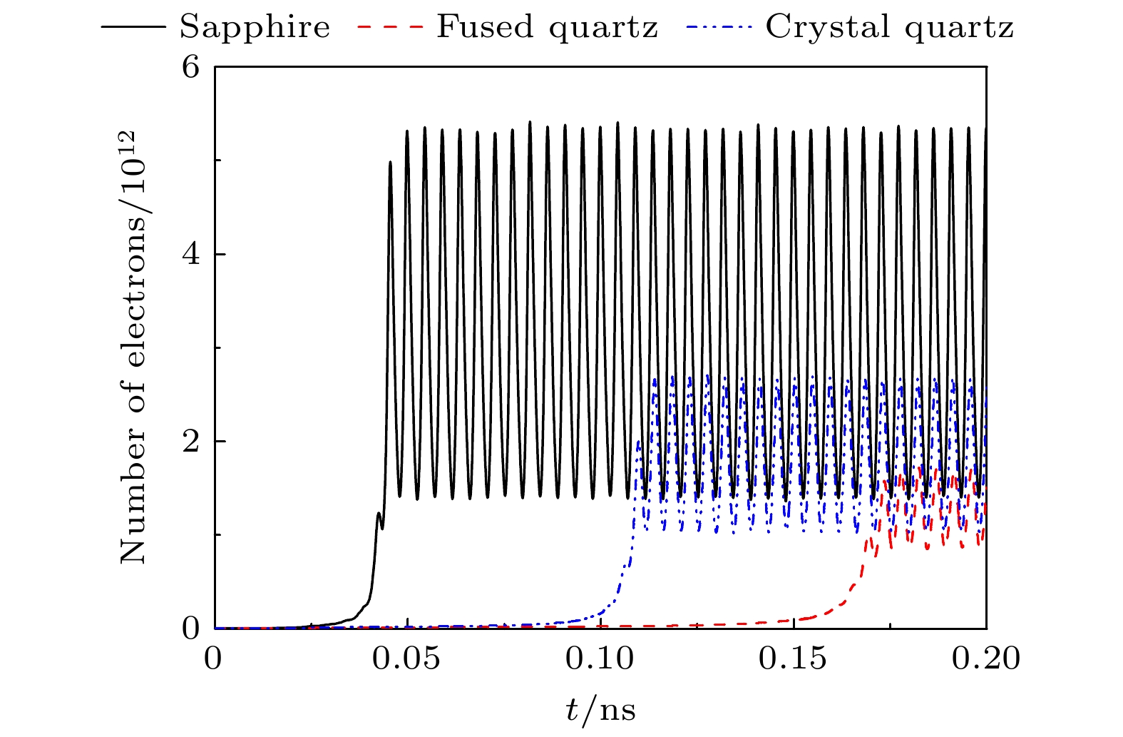
    图8所示为当介质表面处的微波电场振幅 E_\mathrm{{sm}} 取为26 MV \cdot \mathrm{m}^{-1} 时, 蓝宝石、熔融石英和石英晶体表面的次级电子倍增过程的模拟结果. 熔融石英和石英晶体表面附近的电子数量随时间的变化与蓝宝石的情况相似, 即电子数量首先急剧增加, 接着在稳态之后以微波频率的2倍振荡. 在相同的入射电子能量下, 由于蓝宝石的次级电子产额最高, 石英晶体的次之, 熔融石英的次级电子产额最低(见图2), 所以相应的次级电子倍增达到稳态的时间依次增加. 在10—30 eV之间, 次级电子产额曲线与产额为1的直线具有一个交叉点, 称为第一交叉点. 当电子倍增达到稳态时, 平均电子能量在第一交叉点能量附近振荡, 相应的平均次级电子产额等于1. 随着第一交叉点能量的降低, 需要更高的法向静电场来减小电子的渡越时间, 进而使得电子能量在第一交叉点能量附近. 法向静电场正比于介质表面附近的电子数量. 因此, 第一交叉点能量越低, 倍增稳态时的电子数量就越高. 由于熔融石英的第一交叉点能量最高, 石英晶体的次之, 蓝宝石的第一交叉点能量最低, 所以相应的电子数量依次增加, 如图8所示.

    图 8 在介质材料分别为蓝宝石、熔融石英、石英晶体且介质表面附近的微波电场振幅$E_\mathrm{{sm}}$均取为$26\;{\rm{MV}}\cdot \rm{m}^{-1}$下, 电子数量随时间的变化\r\nFig. 8. Number of electrons as a function of time when the dielectric materials are sapphire, fused quartz, and crystal quartz and the amplitude $E_\mathrm{{sm}}$ of the microwave electric field near the dielectric surface is $26\;{\rm{MV}}\cdot \mathrm{m}^{-1}$
    图 8  在介质材料分别为蓝宝石、熔融石英、石英晶体且介质表面附近的微波电场振幅E_\mathrm{{sm}}均取为26\;{\rm{MV}}\cdot \rm{m}^{-1}下, 电子数量随时间的变化
    Fig. 8.  Number of electrons as a function of time when the dielectric materials are sapphire, fused quartz, and crystal quartz and the amplitude E_\mathrm{{sm}} of the microwave electric field near the dielectric surface is 26\;{\rm{MV}}\cdot \mathrm{m}^{-1}

    在次级电子倍增达到稳态之后, 电子数密度的空间分布如图9所示. 图中介质材料和微波电场振幅与图8的情况相同. 尽管次级电子倍增已经达到稳态, 但电子数量仍然以微波频率的2倍振荡. 为了有效比较三种材料下的电子数密度分布, 图9中的电子数密度均取一个微波周期内的平均值. 介质表面附近存在很高的法向静电场, 导致电子的渡越时间很短. 因此, 电子在三种不同的介质材料下均聚集在介质表面( z = 0.15 μm)到 z = 10 μm之间的狭小区域. 尽管如此, 三种介质材料下电子数密度的峰值具有明显的差异.

    图 9 在介质材料分别为蓝宝石、熔融石英、石英晶体且介质表面附近的微波电场振幅$E_\mathrm{{sm}}$均取为$26\;{\rm{MV}}\cdot \mathrm{m}^{-1}$下, 电子倍增达到稳态之后的电子数密度随z的变化\r\nFig. 9. Number density of electrons as a function of z after the secondary electron multipactor reaches steady state. The dielectric materials are sapphire, fused quartz, and crystal quartz and the amplitude $E_\mathrm{{sm}}$ of the microwave electric field near the dielectric surface is $26\;{\rm{MV}}\cdot \mathrm{m}^{-1}$
    图 9  在介质材料分别为蓝宝石、熔融石英、石英晶体且介质表面附近的微波电场振幅E_\mathrm{{sm}}均取为26\;{\rm{MV}}\cdot \mathrm{m}^{-1}下, 电子倍增达到稳态之后的电子数密度随z的变化
    Fig. 9.  Number density of electrons as a function of z after the secondary electron multipactor reaches steady state. The dielectric materials are sapphire, fused quartz, and crystal quartz and the amplitude E_\mathrm{{sm}} of the microwave electric field near the dielectric surface is 26\;{\rm{MV}}\cdot \mathrm{m}^{-1}

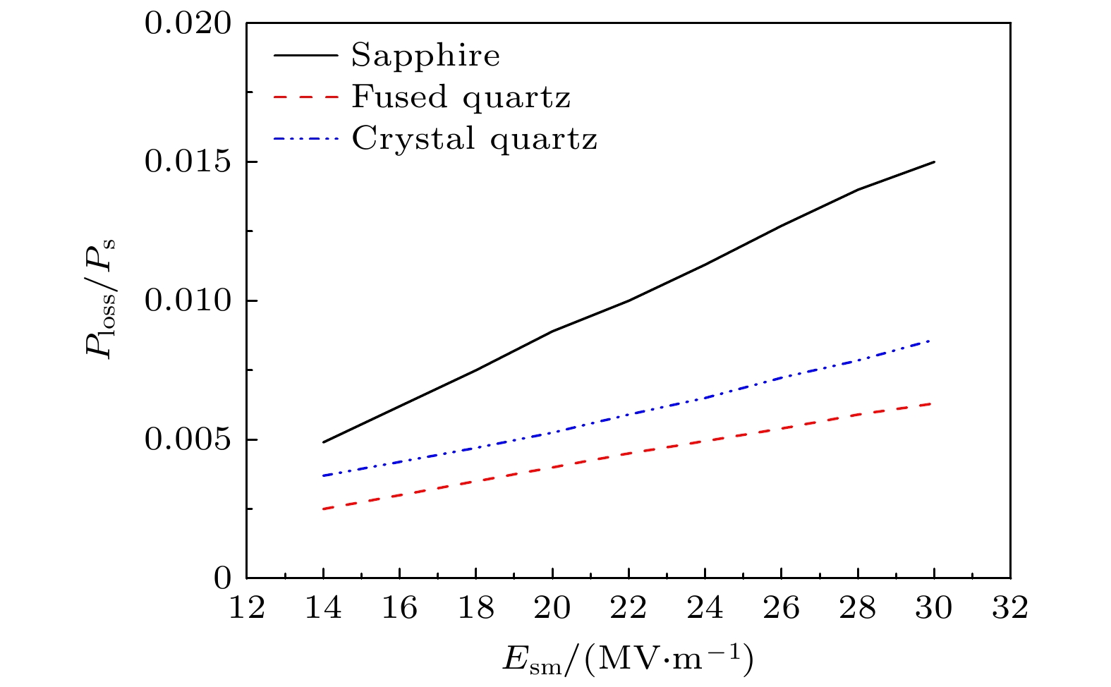
    在次级电子倍增达到稳态之后, 损失功率与介质表面处的功率之比 P_{\mathrm{loss}}/P_{\mathrm{s}} 随微波电场振幅 E_\mathrm{{sm}} 的变化如图10所示. 图中介质材料分别取为蓝宝石、熔融石英、石英晶体. 在这三种不同的介质材料下, P_{\mathrm{loss}}/P_{\mathrm{s}} 均随着 E_\mathrm{{sm}} 缓慢地增加. 由电子倍增引起的损失功率远小于介质表面处的微波功率. 例如, 在介质材料为蓝宝石且 E_\mathrm{{sm}} = 30 MV \cdot \mathrm{m}^{-1} 下, P_{\mathrm{loss}}/P_{\mathrm{s}} 仅为0.015. 尽管三种不同介质材料下的电子数密度分布宽度具有很小的差异, 但是蓝宝石材料下的电子数密度峰值最高, 石英晶体下的次之, 熔融石英下的电子数密度峰值最低(见图9), 以至于相应的 P_{\mathrm{loss}}/P_{\mathrm{s}} 依次减小.

    图 10 在电子倍增达到稳态之后, 损失功率与介质表面处的功率之比$P_{\mathrm{loss}}/P_{\mathrm{s}}$随微波电场振幅$E_\mathrm{{sm}}$的变化, 其中介质材料分别为蓝宝石、熔融石英、石英晶体\r\nFig. 10. Ratio of the loss power to the power at the surface $P_{\mathrm{loss}}/P_{\mathrm{s}}$ as a function of the amplitude of the microwave electric field $E_\mathrm{{sm}}$ after the electron multipactor reaches the steady state. The dielectric materials are sapphire, fused quartz and quartz crystal, respectively
    图 10  在电子倍增达到稳态之后, 损失功率与介质表面处的功率之比P_{\mathrm{loss}}/P_{\mathrm{s}}随微波电场振幅E_\mathrm{{sm}}的变化, 其中介质材料分别为蓝宝石、熔融石英、石英晶体
    Fig. 10.  Ratio of the loss power to the power at the surface P_{\mathrm{loss}}/P_{\mathrm{s}} as a function of the amplitude of the microwave electric field E_\mathrm{{sm}} after the electron multipactor reaches the steady state. The dielectric materials are sapphire, fused quartz and quartz crystal, respectively

    表2所列为微波频率为110 GHz下次级电子倍增阈值的模拟结果与实验数据[21]的比较. 在实验中, 通过逐渐增加介质表面处的微波电场, 若发现损失功率与初始微波功率之比大约超过0.005, 则介质表面处的微波电场被诊断为次级电子倍增阈值. 基于该诊断方法和图10可得到蓝宝石、熔融石英和石英晶体的次级电子倍增阈值大约为14, 25和19 MV \cdot \mathrm{m}^{-1} , 如表2所列. 在这三种不同的介质材料下, 电子倍增阈值的模拟值均靠近相应的实验数据, 但两者存在一定的差异. 在实验中, 次级电子倍增是由高斯波束导致的, 以至于电子数密度在平行于介质表面方向上是非均匀的. 然而, 1D3V电磁粒子模型未考虑电子在平行于介质表面方向上的损失, 以至于过高地估计了电子数量及其引起的能量损失, 如图7所示的蓝宝石的情况. 因此, 次级电子倍增阈值的模拟值低于实验测量值. 另外, 利用电磁粒子模型预测了2.85和9.4 GHz下蓝宝石材料的次级电子倍增阈值, 分别约为0.4和1.2\;{\rm{MV}} \cdot \rm{m}^{-1} . 由表2可见, 110 GHz下蓝宝石材料的次级电子倍增阈值为 14\;{\rm{MV}}\cdot \rm{m}^{-1} . 这表明二次电子倍增阈值随着微波频率的升高而显著增加. 因此, 通过增加微波频率能够抑制次级电子倍增的发生.

    表 2  微波频率为110 GHz下次级电子倍增阈值的模拟结果与实验数据[21]的比较
    Table 2.  Comparison between simulation results and experimental data[21] of secondary electron multipactor threshold at microwave frequency of 110 GHz
    材料类型阈值的模拟结果/(MV·m–1)(P_{\mathrm{loss}}/P_{\mathrm{s}}> 0.005)阈值的实验数据/(MV·m–1)
    蓝宝石1426
    熔融石英2530
    石英晶体1925
    下载: 导出CSV 
    | 显示表格

    本文采用1D3V电磁粒子模型对110 GHz微波介质表面次级电子倍增特性进行了模拟研究. 通过时域有限差分方法求解麦克斯韦方程组, 以分析次级电子倍增对微波功率的影响. 重点研究了不同微波电场和介质材料下次级电子倍增过程及其引起的损失功率. 模拟结果表明: 在次级电子倍增达到稳态之后, 尽管电子数密度高于临界截止数密度, 但是损失功率与介质表面微波功率之比很小, 大约在1%的量级上. 这是因为介质表面附近形成了很高的法向静电场(约为数十MV \cdot \mathrm{m}^{-1} ), 使得电子仅仅分布在若干微米的区域, 远小于相应的趋肤深度. 由次级电子倍增引起的损失功率等于电子对微波功率的吸收与反射之和. 该损失功率随着时间首先增加, 接着在电子倍增达到稳态之后几乎保持不变, 其中电子对微波功率的吸收大于反射功率.

    模拟结果还表明: 随着介质表面处微波电场振幅的增加, 电子倍增达到稳态时的电子数量变得更高, 导致损失功率与介质表面处的微波功率之比增加. 尽管如此, 损失功率远小于介质表面处的微波功率, 两者的比值大约在0.01附近. 该比值随微波电场振幅的变化趋势与实验结果一致, 但前者较大. 这是由于实验中采用高斯波束导致次级电子倍增现象的发生, 而在1D3V电磁粒子模拟中未考虑平行于介质表面上的电子损失, 以至于过高地估计了电子数量及其引起的损失功率. 由于不同材料的次级电子产额曲线具有明显的差异, 所以电子倍增达到稳态的时间随着介质材料改变. 在次级电子倍增达到稳态之后, 蓝宝石表面附近的电子数量最高, 石英晶体的次之, 熔融石英的电子数量最低, 这导致相应的损失功率与介质表面处的微波功率之比依次减小. 依据实验诊断方法, 倍增阈值被定义为损失功率与介质表面处微波功率之比大于0.005的临界微波电场振幅. 在这三种不同的介质材料下, 倍增阈值的模拟值均靠近相应的实验测量值, 然而前者更低. 该差异主要归因于1D3V电磁粒子模型未考虑实验中平行于介质表面的电子损失, 以至于过高地估计了电子数量及其引起的损失功率.

    [1]

    常超 2018 科学通报 63 1391

    Chang C 2018 Chin Sci. Bull. 63 1391

    [2]

    杨德文, 陈昌华, 史彦超, 肖仁珍, 滕雁, 范志强, 刘文元, 宋志敏, 孙钧 2020 物理学报 69 164102Google Scholar

    Yang D W, Chen C H, Shi Y C, Xiao R Z, Teng Y, Fan Z Q, Liu W Y, Song Z M, Sun J 2020 Acta Phys. Sin. 69 164102Google Scholar

    [3]

    刘振帮, 黄华, 金晓, 王腾钫, 李士锋 2020 物理学报 69 218401Google Scholar

    Liu Z B, Huang H, Jin X, Wang T F, Li S F 2020 Acta Phys. Sin. 69 218401Google Scholar

    [4]

    Chang C, Liu G, Tang C, Chen C, Fang J 2011 Phys. Plasmas 18 055702Google Scholar

    [5]

    蔡利兵, 王建国 2011 物理学报 18 025217Google Scholar

    Cai L B, Wang J G 2011 Acta Phys. Sin. 18 025217Google Scholar

    [6]

    Zhao P, Wang R, Guo L 2022 Plasma Sources Sci. Technol. 31 095005Google Scholar

    [7]

    Kishek R A, Lau Y Y 1998 Phys. Rev. Lett. 80 193Google Scholar

    [8]

    Kim H C, Verboncoeur J P 2006 Phys. Plasmas 13 123506Google Scholar

    [9]

    蔡利兵, 王建国 2010 物理学报 59 1143Google Scholar

    Cai L B, Wang J G 2010 Acta Phys. Sin. 59 1143Google Scholar

    [10]

    李爽, 常超, 王建国, 刘彦升, 朱梦, 郭乐田, 谢佳玲 2015 物理学报 64 137701Google Scholar

    Li S, Chang C, Wang J G, Liu Y S, Zhu M, Guo L T, Xie J L 2015 Acta Phys. Sin. 64 137701Google Scholar

    [11]

    左春彦, 高飞, 戴忠玲, 王友年 2018 物理学报 67 225201Google Scholar

    Zuo C Y, Gao F, Dai Z L, Wang Y N 2018 Acta Phys. Sin. 67 225201Google Scholar

    [12]

    Iqbal A, Wong P Y, Wen D Q, Lin S, Verboncoeur J, Zhang P 2020 Phys. Rev. E 102 043201Google Scholar

    [13]

    董烨, 周前红, 董志伟, 杨温渊, 周海京, 孙会芳 2013 强激光与粒子束 25 950Google Scholar

    Dong Y, Zhou Q H, Dong Z W, Yang W Y, Zhou H J, Sun H F 2013 High Power Laser and Particle Beams 25 950Google Scholar

    [14]

    董烨, 董志伟, 周前红, 杨温渊, 周海京 2014 物理学报 63 067901Google Scholar

    Dong Y, Dong Z W, Zhou Q H, Yang W Y, Zhou H J 2014 Acta Phys. Sin. 63 067901Google Scholar

    [15]

    董烨, 周前红, 杨温渊, 董志伟, 周海京 2014 物理学报 63 185206Google Scholar

    Dong Y, Zhou Q H, Yang W Y, Dong Z W, Zhou H J 2014 Acta Phys. Sin. 63 185206Google Scholar

    [16]

    Chang C, Liu G Z, Huang H J, Chen C, Fang J 2009 Phys. Plasmas 16 083501Google Scholar

    [17]

    Chang C, Huang H J, Liu G Z, Chen C H, Hou Q, Fang J Y 2009 J. Appl. Phys. 105 123305Google Scholar

    [18]

    Chang C, Fang J Y, Zhang Z Q, Chen C, Tang C, Jin Q 2010 Appl. Phys. Lett. 97 141501Google Scholar

    [19]

    Chang C, Liu Y S, Verboncoeur J, Chen C H, Guo L T, Li S, Wu X L 2015 Appl. Phys. Lett. 106 014102Google Scholar

    [20]

    翁明, 谢少毅, 殷明, 曹猛 2020 物理学报 69 087901Google Scholar

    Weng M, Xie S Y, Yin M, Cao M 2020 Acta Phys. Sin. 69 087901Google Scholar

    [21]

    Schaub S C, Shapiro M A, Temkin R J 2019 Phys. Rev. Lett. 123 175001Google Scholar

    [22]

    Birdsall C K 1991 IEEE Trans. Plasma Sci. 19 65Google Scholar

    [23]

    Taflove A, Hagness S C 2000 Computational Electrodynamics: The Finite-Difference Time Domain Method (Boston, MA: Artech House Publishers) pp10−150

    [24]

    Vaughan J R M 1989 IEEE Trans. Electron Devices 36 1963Google Scholar

    [25]

    Cheng G, Liu L 2010 IEEE Trans. Plasma Sci. 38 3109Google Scholar

  • 图 1  高功率微波作用下介质表面次级电子倍增的示意图

    Figure 1.  Schematic diagram of secondary electron multipactor on dielectric surface under high power microwave

    图 2  在入射角等于{\pi}/{2}以及介质材料分别为蓝宝石、熔融石英和石英晶体下, 次级电子产额δ随入射电子能量的变化

    Figure 2.  Change of secondary electron yield δ with incident electron energy when the incident angle is {\pi}/{2} and the dielectric materials are sapphire, fused quartz and crystal quartz respectively

    图 3  在介质材料为蓝宝石, 介质表面附近的微波电场振幅E_\mathrm{{sm}}取为不同值下, (a)平均电子能量\langle\varepsilon_\mathrm{e}\rangle和(b)电子数量随时间的变化

    Figure 3.  Variation of (a) mean electron energy \langle\varepsilon_\mathrm{e}\rangle and (b) number of electrons over time when the dielectric material is sapphire and the amplitude E_\mathrm{{sm}} of microwave electric field near the dielectric surface takes different values

    图 4  在次级电子倍增达到稳态之后, (a)电子数密度n_\mathrm{e}和(b)法向静电场E_{\mathrm{dc}}z的变化, 其中模拟条件与图3相同

    Figure 4.  Spatial distributions of (a) electron number density n_\mathrm{e} and (b) the normal electrostatic field E_{\mathrm{dc}} after the secondary electron multipactor reaches the steady state, where the simulation conditions are the same as Fig. 3

    图 5  电子倍增发生之前的微波电场振幅与电子倍增稳态之后的电场振幅之间的比较, 其中介质材料为蓝宝石, 表面处的电场振幅为22 MV/m

    Figure 5.  Comparison of microwave electric field amplitude without electron multipactor with that after the secondary electron multipactor reaches the steady state. The dielectric material is sapphire, and the electric field amplitude at the surface is 22 MV/m

    图 6  在介质材料为蓝宝石, 介质表面附近的微波电场振幅E_\mathrm{{sm}}取为不同值下, (a)反射功率与入射功率之比P_{\mathrm{r}}/P_{\mathrm{in}}, (b)吸收功率与入射功率之比P_{\mathrm{a}}/P_{\mathrm{in}}和(c)损失功率与入射功率之比P_{\mathrm{loss}}/P_{\mathrm{in}}随时间的变化

    Figure 6.  (a) The ratio P_{\mathrm{r}}/P_{\mathrm{in}} of reflected power to incident power, (b) the ratio P_{\mathrm{a}}/P_{\mathrm{in}} of absorbed power to incident power, and (c) the ratio P_{\mathrm{loss}}/P_{\mathrm{in}} of loss power to incident power as a function of time when the dielectric material is sapphire and the amplitude E_\mathrm{{sm}} of microwave electric field near the dielectric surface takes different values

    图 7  在介质材料为蓝宝石, 介质表面附近的微波电场振幅E_\mathrm{{sm}}取为不同值下, 损失功率与介质表面处功率之比的模拟值与实验数据的比较

    Figure 7.  Comparison between simulated value and experimental data of the ratio of loss power to power near dielectric surface when the dielectric material is sapphire and the amplitude E_\mathrm{{sm}} of microwave electric field near the dielectric surface takes different values

    图 8  在介质材料分别为蓝宝石、熔融石英、石英晶体且介质表面附近的微波电场振幅E_\mathrm{{sm}}均取为26\;{\rm{MV}}\cdot \rm{m}^{-1}下, 电子数量随时间的变化

    Figure 8.  Number of electrons as a function of time when the dielectric materials are sapphire, fused quartz, and crystal quartz and the amplitude E_\mathrm{{sm}} of the microwave electric field near the dielectric surface is 26\;{\rm{MV}}\cdot \mathrm{m}^{-1}

    图 9  在介质材料分别为蓝宝石、熔融石英、石英晶体且介质表面附近的微波电场振幅E_\mathrm{{sm}}均取为26\;{\rm{MV}}\cdot \mathrm{m}^{-1}下, 电子倍增达到稳态之后的电子数密度随z的变化

    Figure 9.  Number density of electrons as a function of z after the secondary electron multipactor reaches steady state. The dielectric materials are sapphire, fused quartz, and crystal quartz and the amplitude E_\mathrm{{sm}} of the microwave electric field near the dielectric surface is 26\;{\rm{MV}}\cdot \mathrm{m}^{-1}

    图 10  在电子倍增达到稳态之后, 损失功率与介质表面处的功率之比P_{\mathrm{loss}}/P_{\mathrm{s}}随微波电场振幅E_\mathrm{{sm}}的变化, 其中介质材料分别为蓝宝石、熔融石英、石英晶体

    Figure 10.  Ratio of the loss power to the power at the surface P_{\mathrm{loss}}/P_{\mathrm{s}} as a function of the amplitude of the microwave electric field E_\mathrm{{sm}} after the electron multipactor reaches the steady state. The dielectric materials are sapphire, fused quartz and quartz crystal, respectively

    表 1  介质材料的次级电子发射参数[21]和电磁参数

    Table 1.  Secondary electron emission parameters[21] and electromagnetic parameters of dielectric materials

    材料类型次级电子发射参数 电磁参数
    \delta_{\mathrm{max0}}\varepsilon_{\mathrm{max0}}/eV \epsilon_{\mathrm{r}}\mu_\mathrm{r}
    蓝宝石7.8650101.0
    熔融石英2.94203.61.0
    石英晶体3.84004.61.0
    DownLoad: CSV

    表 2  微波频率为110 GHz下次级电子倍增阈值的模拟结果与实验数据[21]的比较

    Table 2.  Comparison between simulation results and experimental data[21] of secondary electron multipactor threshold at microwave frequency of 110 GHz

    材料类型阈值的模拟结果/(MV·m–1)(P_{\mathrm{loss}}/P_{\mathrm{s}}> 0.005)阈值的实验数据/(MV·m–1)
    蓝宝石1426
    熔融石英2530
    石英晶体1925
    DownLoad: CSV
  • [1]

    常超 2018 科学通报 63 1391

    Chang C 2018 Chin Sci. Bull. 63 1391

    [2]

    杨德文, 陈昌华, 史彦超, 肖仁珍, 滕雁, 范志强, 刘文元, 宋志敏, 孙钧 2020 物理学报 69 164102Google Scholar

    Yang D W, Chen C H, Shi Y C, Xiao R Z, Teng Y, Fan Z Q, Liu W Y, Song Z M, Sun J 2020 Acta Phys. Sin. 69 164102Google Scholar

    [3]

    刘振帮, 黄华, 金晓, 王腾钫, 李士锋 2020 物理学报 69 218401Google Scholar

    Liu Z B, Huang H, Jin X, Wang T F, Li S F 2020 Acta Phys. Sin. 69 218401Google Scholar

    [4]

    Chang C, Liu G, Tang C, Chen C, Fang J 2011 Phys. Plasmas 18 055702Google Scholar

    [5]

    蔡利兵, 王建国 2011 物理学报 18 025217Google Scholar

    Cai L B, Wang J G 2011 Acta Phys. Sin. 18 025217Google Scholar

    [6]

    Zhao P, Wang R, Guo L 2022 Plasma Sources Sci. Technol. 31 095005Google Scholar

    [7]

    Kishek R A, Lau Y Y 1998 Phys. Rev. Lett. 80 193Google Scholar

    [8]

    Kim H C, Verboncoeur J P 2006 Phys. Plasmas 13 123506Google Scholar

    [9]

    蔡利兵, 王建国 2010 物理学报 59 1143Google Scholar

    Cai L B, Wang J G 2010 Acta Phys. Sin. 59 1143Google Scholar

    [10]

    李爽, 常超, 王建国, 刘彦升, 朱梦, 郭乐田, 谢佳玲 2015 物理学报 64 137701Google Scholar

    Li S, Chang C, Wang J G, Liu Y S, Zhu M, Guo L T, Xie J L 2015 Acta Phys. Sin. 64 137701Google Scholar

    [11]

    左春彦, 高飞, 戴忠玲, 王友年 2018 物理学报 67 225201Google Scholar

    Zuo C Y, Gao F, Dai Z L, Wang Y N 2018 Acta Phys. Sin. 67 225201Google Scholar

    [12]

    Iqbal A, Wong P Y, Wen D Q, Lin S, Verboncoeur J, Zhang P 2020 Phys. Rev. E 102 043201Google Scholar

    [13]

    董烨, 周前红, 董志伟, 杨温渊, 周海京, 孙会芳 2013 强激光与粒子束 25 950Google Scholar

    Dong Y, Zhou Q H, Dong Z W, Yang W Y, Zhou H J, Sun H F 2013 High Power Laser and Particle Beams 25 950Google Scholar

    [14]

    董烨, 董志伟, 周前红, 杨温渊, 周海京 2014 物理学报 63 067901Google Scholar

    Dong Y, Dong Z W, Zhou Q H, Yang W Y, Zhou H J 2014 Acta Phys. Sin. 63 067901Google Scholar

    [15]

    董烨, 周前红, 杨温渊, 董志伟, 周海京 2014 物理学报 63 185206Google Scholar

    Dong Y, Zhou Q H, Yang W Y, Dong Z W, Zhou H J 2014 Acta Phys. Sin. 63 185206Google Scholar

    [16]

    Chang C, Liu G Z, Huang H J, Chen C, Fang J 2009 Phys. Plasmas 16 083501Google Scholar

    [17]

    Chang C, Huang H J, Liu G Z, Chen C H, Hou Q, Fang J Y 2009 J. Appl. Phys. 105 123305Google Scholar

    [18]

    Chang C, Fang J Y, Zhang Z Q, Chen C, Tang C, Jin Q 2010 Appl. Phys. Lett. 97 141501Google Scholar

    [19]

    Chang C, Liu Y S, Verboncoeur J, Chen C H, Guo L T, Li S, Wu X L 2015 Appl. Phys. Lett. 106 014102Google Scholar

    [20]

    翁明, 谢少毅, 殷明, 曹猛 2020 物理学报 69 087901Google Scholar

    Weng M, Xie S Y, Yin M, Cao M 2020 Acta Phys. Sin. 69 087901Google Scholar

    [21]

    Schaub S C, Shapiro M A, Temkin R J 2019 Phys. Rev. Lett. 123 175001Google Scholar

    [22]

    Birdsall C K 1991 IEEE Trans. Plasma Sci. 19 65Google Scholar

    [23]

    Taflove A, Hagness S C 2000 Computational Electrodynamics: The Finite-Difference Time Domain Method (Boston, MA: Artech House Publishers) pp10−150

    [24]

    Vaughan J R M 1989 IEEE Trans. Electron Devices 36 1963Google Scholar

    [25]

    Cheng G, Liu L 2010 IEEE Trans. Plasma Sci. 38 3109Google Scholar

  • [1] Shu Pan-Pan, Zhao Peng-Cheng. Particle-in-cell-Monte Carlo collision simulation study on gas side breakdown characteristics of high-power microwave dielectric window. Acta Physica Sinica, 2024, 73(23): 235101. doi: 10.7498/aps.73.20241177
    [2] Huang Hua, Wu Yang, Liu Zhen-Bang, Yuan Huan, He Hu, Li Le-Le, Li Zheng-Hong, Jin Xiao, Ma Hong-Ge. Review on high power microwave device with locked frequency and phase. Acta Physica Sinica, 2018, 67(8): 088402. doi: 10.7498/aps.67.20172684
    [3] Zuo Chun-Yan, Gao Fei, Dai Zhong-Ling, Wang You-Nian. PIC/MCC simulation of breakdown dynamics inside high power microwave output window. Acta Physica Sinica, 2018, 67(22): 225201. doi: 10.7498/aps.67.20181260
    [4] Li Zhi-Peng, Li Jing, Sun Jing, Liu Yang, Fang Jin-Yong. High power microwave damage mechanism on high electron mobility transistor. Acta Physica Sinica, 2016, 65(16): 168501. doi: 10.7498/aps.65.168501
    [5] Wei Jin-Jin, Zhou Dong-Fang, Yu Dao-Jie, Hu Tao, Hou De-Ting, Zhang De-Wei, Lei Xue, Hu Jun-Jie. Seed electron production from O- detachment in high power microwave air breakdown. Acta Physica Sinica, 2016, 65(5): 055202. doi: 10.7498/aps.65.055202
    [6] Tang Tao. Numerical validation study of high power microwave soil breakdown. Acta Physica Sinica, 2015, 64(4): 045203. doi: 10.7498/aps.64.045203
    [7] Dong Ye, Dong Zhi-Wei, Zhou Qian-Hong, Yang Wen-Yuan, Zhou Hai-Jing. Particle-in-cell simulation on effect of outgassing on flashover and breakdown on dielectric surface in high-power microwave environment. Acta Physica Sinica, 2014, 63(2): 027901. doi: 10.7498/aps.63.027901
    [8] Zhang Xue, Wang Yong, Fan Jun-Jie, Zhang Rui. Numerical simulation of multipactor phenomenon on the surface of cylinder window disk. Acta Physica Sinica, 2014, 63(22): 227901. doi: 10.7498/aps.63.227901
    [9] Zhang Xue, Wang Yong, Fan Jun-Jie, Zhu Fang, Zhang Rui. Multipactor phenomenon between metal anddielectric window. Acta Physica Sinica, 2014, 63(16): 167901. doi: 10.7498/aps.63.167901
    [10] Zhang Xue, Fan Jun-Jie, Wang Yong. Suppression effect of periodic semicircle groove disk on multipactor. Acta Physica Sinica, 2014, 63(22): 227902. doi: 10.7498/aps.63.227902
    [11] Dong Ye, Dong Zhi-Wei, Yang Wen-Yuan, Zhou Qian-Hong, Zhou Hai-Jing. Effects of transverse electromagnetic field distribution in the multipactor discharge on dielectric window surface. Acta Physica Sinica, 2013, 62(19): 197901. doi: 10.7498/aps.62.197901
    [12] Zhou Dong-Fang, Yu Dao-Jie, Yang Jian-Hong, Hou De-Ting, Xia Wei, Hu Tao, Lin Jing-Yu, Rao Yu-Ping, Wei Jin-Jin, Zhang De-Wei, Wang Li-Ping. Theoretical and experimental investigation of air breakdown on single high power microwave based on the mixed-atmosphere propagation model. Acta Physica Sinica, 2013, 62(1): 014207. doi: 10.7498/aps.62.014207
    [13] Cai Li-Bing, Wang Jian-Guo, Zhu Xiang-Qin, Wang Yue, Xuan Chun, Xia Hong-Fu. Effects of an external magnetic field on multipactor on a dielectric surface. Acta Physica Sinica, 2012, 61(7): 075101. doi: 10.7498/aps.61.075101
    [14] Yang Chao, Liu Da-Gang, Zhou Jun, Liao Chen, Peng Kai, Liu Sheng-Gang. Three-dimensional particle-in-cell simulation studies on a new radial three-cavity coaxial virtual cathode oscillator. Acta Physica Sinica, 2011, 60(8): 084102. doi: 10.7498/aps.60.084102
    [15] Wu Yang, Xu Zhou, Xu Yong, Jin Xiao, Chang An-Bi, Li Zheng-Hong, Huang Hua, Liu Zhong, Luo Xiong, Ma Qiao-Sheng, Tang Chuan-Xiang. Experimental study on a high power microwave amplifier driven by low rf power. Acta Physica Sinica, 2011, 60(4): 044102. doi: 10.7498/aps.60.044102
    [16] Wang Gan-Ping, Xiang Fei, Tan Jie, Cao Shao-Yun, Luo Min, Kang Qiang, Chang An-Bi. Investigation in discharge progress of a long pulse high power microwave-driven source. Acta Physica Sinica, 2011, 60(7): 072901. doi: 10.7498/aps.60.072901
    [17] Cai Li-Bing, Wang Jian-Guo, Zhu Xiang-Qin. Numerical simulation of multipactor on dielectric surface in high direct current field. Acta Physica Sinica, 2011, 60(8): 085101. doi: 10.7498/aps.60.085101
    [18] Cai Li-Bing, Wang Jian-Guo. Effects of the microwave magnetic field and oblique incident microwave on multipactor discharge on a dielectric surface. Acta Physica Sinica, 2010, 59(2): 1143-1147. doi: 10.7498/aps.59.1143
    [19] Cai Li-Bing, Wang Jian-Guo. Numerical simulation of the breakdown on HPM dielectric surface. Acta Physica Sinica, 2009, 58(5): 3268-3273. doi: 10.7498/aps.58.3268
    [20] Li Zheng-Hong, Meng Fan-Bao, Chang An-Bi, Huang Hua, Ma Qiao-Sheng. Investigation of bitron as a high power microwave oscillator. Acta Physica Sinica, 2005, 54(8): 3578-3583. doi: 10.7498/aps.54.3578
Metrics
  • Abstract views:  3916
  • PDF Downloads:  75
Publishing process
  • Received Date:  22 November 2022
  • Accepted Date:  12 March 2023
  • Available Online:  22 March 2023
  • Published Online:  05 May 2023

/

返回文章
返回