


SPECIAL TOPIC—Novel physical properties of functional oxide thin films

2023, 72 (9): 096801.
doi: 10.7498/aps.72.20222266
Abstract +
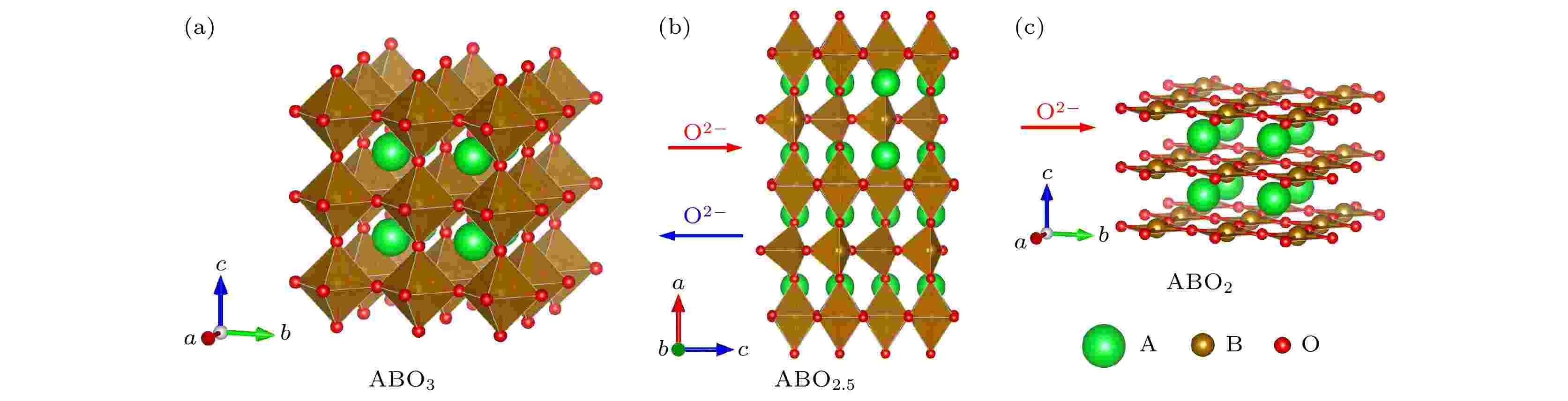
Perovskite transition-metal oxides can undergo significant structural topological phase transition between perovskite structure, brownmillerite structure, and infinite-layer structure under the external field through the gain and loss of the oxygen ions, accompanied with significant changes in physical properties such as transportation, magnetism, and optics. Topotactic phase transformation allows structural transition without losing the crystalline symmetry of the parental phase and provides an effective platform for utilizing the redox reaction and oxygen diffusion within transition metal oxides, and establishing great potential applications in solid oxide fuel cells, oxygen sensors, catalysis, intelligent optical windows, and neuromorphic devices. In this work, we review the recent research progress of manipulating the topological phase transition of the perovskite-type oxide films and regulating their physical properties, mainly focusing on tuning the novel physical properties of these typical films through strong interaction between the lattice and electronic degrees of freedom by the action of external fields such as strain, electric field, optical field, and temperature field. For example, a giant photoinduced structure distortion in SrCoO2.5 thin film excited by photons is observed to be higher than any previously reported results in the other transition metal oxide films. The SrFeO2 films undergo an insulator-to-metal transition when the strain state changes from compressive state to tensile state. It is directly observed that perovskite SrFeO3 nanofilament is formed under the action of electric field and extends almost through the brownmillerite SrFeO2.5 matrix in the ON state and is ruptured in the OFF state, unambiguously revealing a filamentary resistance switching mechanism. Utilizing in situ electrical scanning transmission electron microscopy, the transformation from brownmillerite SrFeO2.5 to infinite-layer SrFeO2 under electric field can be directly visualized with atomic resolution. We also clarify the relationship between the microscopic coupling mechanism and the macroscopic quantum properties of charges, lattices, orbits, spin, etc. Relevant research is expected to provide a platform for new materials, new approaches and new ideas for developing high-sensitivity and weak-field response electronic devices based on functional oxides. These findings about the topological phase transition in perovskite oxide films can expand the research scope of material science, and have important significance in exploring new states of matters and studying quantum critical phenomena.
2023, 72 (9): 097401.
doi: 10.7498/aps.72.20230044
Abstract +
Oxide interfaces manifest many fascinating phenomena with synergetic correlations among multiple degrees of freedom, including the interplay of broken symmetry, lattice mismatch, charge transfer, spatial confinement. In particular, the interface superconductivity in oxide heterostructure has attracted extensive attention due to the rich underlying physical connotations. The interfaces not only provide alternative research platforms with respect to the bulk material counterpart for exploring new superconductors and investigating superconducting mechanisms, but also create new opportunities for applying superconductors to future electronic devices. In recent years, owing to the rapid development of heteroepitaxial techniques and accurate characterization methods, researchers have found quasi-two-dimensional interface superconductivity in various oxide heterostructures and revealed numerous novel quantum phenomena associated with interface superconductivity, which not only promotes the development of condensed matter physics, but also lays important foundation for the practical application of interface superconductivity. In this brief review, we mainly focus on the quasi-two-dimensional superconductivity at oxide interface. Taking the typical quasi-two-dimensional superconductivity at the LaAlO3/SrTiO3 interface and copper oxides such as La2CuO4/La1.56Sr0.44CuO4 for example, we summarize and examine some novel physical phenomena with interface superconductivity in complex oxide heterostructures. Then we address the related problems that remain to be solved, and finally we prospect the possible future development of the interface superconductivity.
2023, 72 (9): 097502.
doi: 10.7498/aps.72.20230206
Abstract +
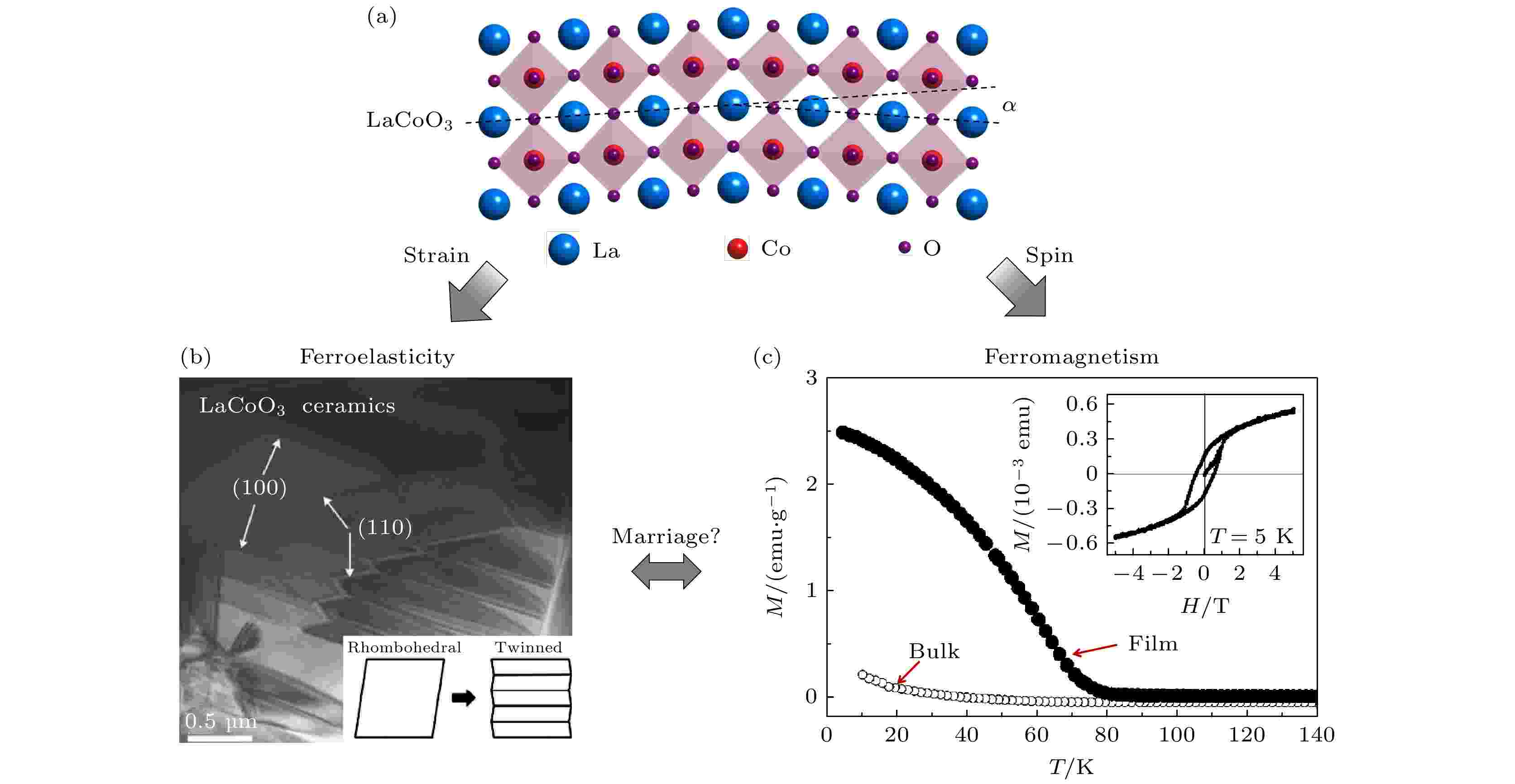
Strongly correlated electronic system contains strong coupling among multi-order parameters and is easy to efficiently tune by external field. Cobaltite (LaCoO3) is a typical multiferroic (ferroelastic and ferromagnetic) material, which has been extensively investigated over decades. Conventional research on cobaltites has focused on the ferroelastic phase transition and structure modulation under stress. Recently, researchers have discovered that cobaltite thin films undergo a paramagnetic-to-ferromagnetic phase transition under tensile strain, however, its origin has been controversial over decades. Some experimental evidence shows that stress leads the valence state of cobalt ions to decrease, and thus producing spin state transition. Other researchers believe that the stress-induced nano-domain structure will present a long-range ordered arrangement of high spin states, which is the main reason for producing the ferromagnetism of cobalt oxide films. In this paper, we review a series of recent researches of the strong correlation between spin and lattice degrees of freedom in cobalt oxide thin films and heterojunctions. The reversible spin state transition in cobalt oxide film is induced by structural factors such as thin-film thickness, lattice mismatch stress, crystal symmetry, surface morphology, interfacial oxygen ion coordination, and oxygen octahedral tilting while the valence state of cobalt ions is kept unchanged, and thus forming highly adjustable macroscopic magnetism. Furthermore, the atomic-level precision controllable film growth technology is utilized to construct single cell layer cobaltite superlattices, thereby achieving ultra-thin two-dimensional magnetic oxide materials through efficient structure regulation. These advances not only clarified the strong coupling between lattice and spin order parameters in the strongly correlated electronic system, but also provided excellent candidate for the realization of ultra-thin room temperature ferromagnets that are required by oxide spintronic devices.
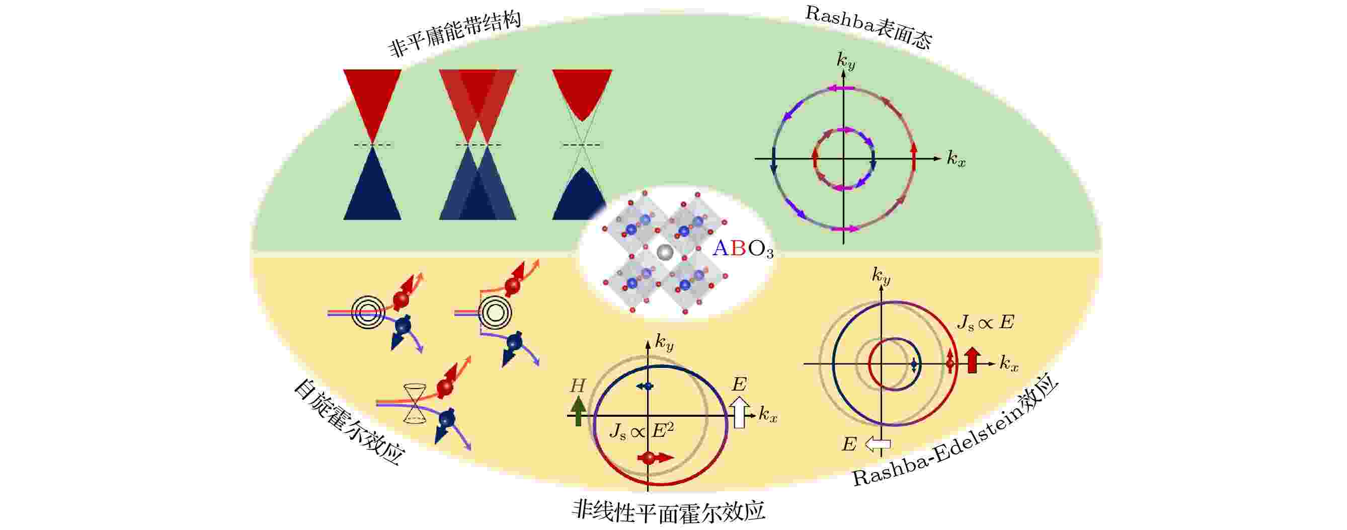
Research progress of novel quantum states and charge-spin interconversion in transition metal oxides
2023, 72 (9): 097702.
doi: 10.7498/aps.72.20222219
Abstract +
For efficient storage and processing of massive data in the information technology era, spintronic device attracts tremendous attention due to its low power consumption and non-volatile feature. Spin source material, which can efficiently generates spin current, is an important constituent of novel spin-orbit torque device. The efficiency of spin current generation in spin source material directly determines the performances of various spintronic devices. In the past two decades, great progress has been made in exploring high-efficient spin source material systems and understanding the relevant physical mechanisms. A wide variety of materials are explored, ranging from traditional heavy metals and semiconductors to topological insulators and two-dimensional (2D) materials. Recently, the material family of transition metal oxides attracts tremendous attention due to its efficient and highly tunable charge-spin conversion intimately related to its emerging novel quantum states and electronic structure. The mechanism of charge-spin conversion generally has two contributions: the bulk spin Hall effect and the spin-momentum locked interface with inversion symmetry breaking. Novel electronic structures such as topological band structures and spin-momentum locked surface states can realize efficient charge-spin conversion. For example, the Weyl points in SrRuO3 and the topological Dirac nodal line in SrIrO3 are predicted to give rise to a large Berry curvature and corresponding spin Hall conductance; the topological surface states can generate spin accumulation due to spin-momentum locking; the Rashba states at the oxide interface such as the 2D electron gas in SrTiO3 and KTaO3 can generate spin current by Rashba-Edelstein effect. Furthermore, the entanglement of various degrees of freedom, including spin, charge, lattice and orbit in transition metal oxides lead to the electronic structure being highly tunable by various methods including gate voltage, substrate constraint, thickness, interface engineering, etc. Therefore, charge-spin conversion in transition metal oxides is of great significance for both modulating of novel electronic structure in fundamental research and exploring its promising potential in future spintronic devices. In this review, we focus on introducing aspects of exotic electronic structures, spin transport mechanism, charge-spin interconversion characterization, efficiency and manipulation in transition metal oxides, and giving a prospect on the future development trend.
2023, 72 (9): 097703.
doi: 10.7498/aps.72.20222221
Abstract +
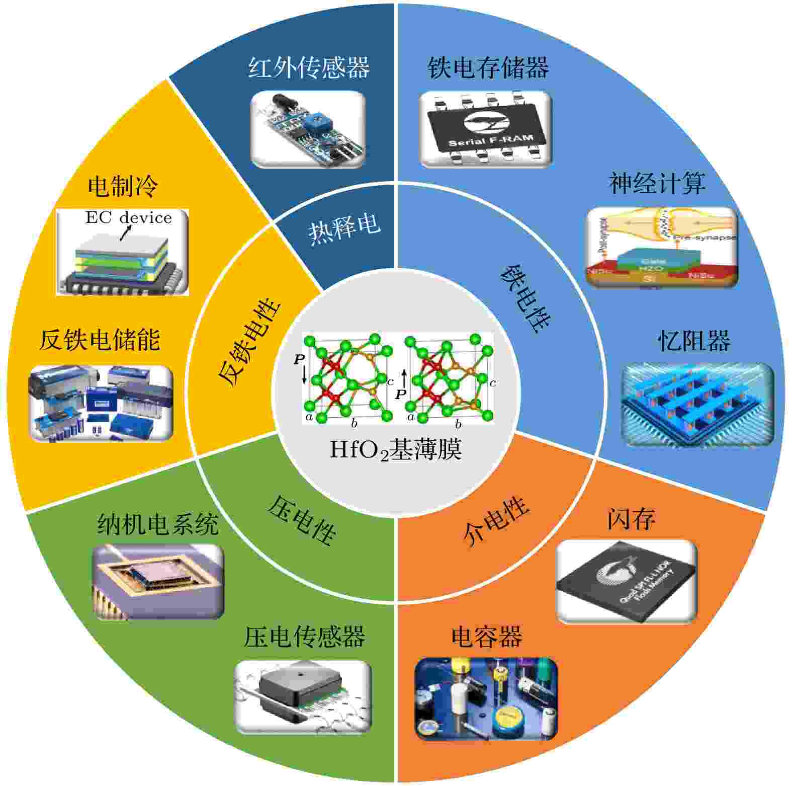
The rapid developments of big data, the internet of things, and artificial intelligence have put forward more and more requirements for memory chips, logic chips and other electronic components. This study introduces the ferroelectric origin of HfO2-based ferroelectric film and explains how element doping, defects, stresses, surfaces and interfaces, regulate and enhance the ferroelectric polarization of the film. It is widely accepted that the ferroelectricity of HfO2-based ferroelectric film originates from the metastable tetragonal phase. The ferroelectricity of the HfO2-based film can be enhanced by doping some elements such as Zr, Si, Al, Gd, La, and Ta, thereby affecting the crystal structure symmetry. The introduction of an appropriate number of oxygen vacancy defects can reduce the potential barrier of phase transition between the tetragonal phase and the monoclinic phase, making the monoclinic phase easy to transition to tetragonal ferroelectric phase. The stability of the ferroelectric phase can be improved by some methods, including forming the stress between the substrate and electrode, reducing the film thickness, constructing a nanolayered structure, and reducing the annealing temperature. Compared with perovskite oxide ferroelectric thin films, HfO2-based films have the advantages of good complementary-metal-oxide-semiconductor compatibility and strong ferroelectricity at nanometer thickness, so they are expected to be used in ferroelectric memory. The HfO2-based 1T1C memory has the advantages of fast reading and writing speed, more than reading and writing 1012 times, and high storage density, and it is the fast reading and writing speed that the only commercial ferroelectric memory possesses at present. The 1T ferroelectric field effect transistor memory has the advantages of non-destructive reading and high storage density. Theoretically, these memories can achieve the same storage density as flash memory, more than reading 1010 times, the fast reading/writing speed, low operating voltage, and low power consumption, simultaneously. Besides, ferroelectric negative capacitance transistor can obtain a subthreshold swing lower than 60 mV/dec, which greatly reduces the power consumption of integrated circuits and provides an excellent solution for further reducing the size of transistors. Ferroelectric tunnel junction has the advantages of small size and easy integration since the tunneling current can be largely adjusted through ferroelectric polarization switching. In addition, the HfO2-based field effect transistors can be used to simulate biological synapses for applications in neural morphology calculations. Moreover, the HfO2-based films also have broad application prospects in antiferroelectric energy storage, capacitor dielectric energy storage, memristor, piezoelectric, and pyroelectric devices, etc. Finally, the current challenges and future opportunities of the HfO2-based thin films and devices are analyzed.
2023, 72 (9): 097704.
doi: 10.7498/aps.72.20230389
Abstract +
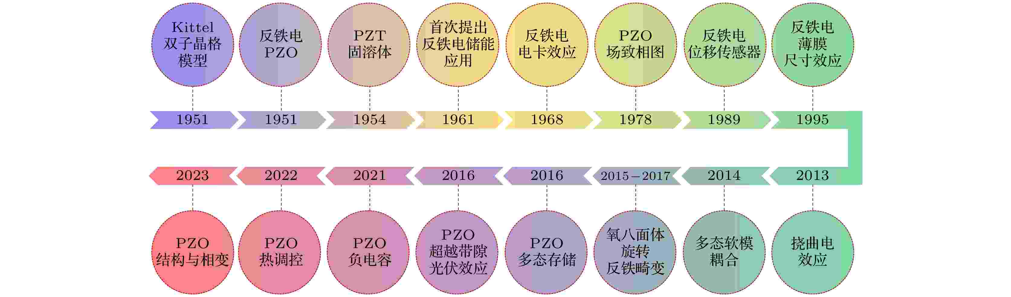
It has been more than 70 years since the first anti-ferroelectric was discovered. Its unique electric-field-induced phase transition behavior shows great potential applications in the fields of energy storage, electrocaloric, negative capacitance, thermal switching, etc. With the development of advanced synthesis technology and the trend of miniaturization and integration of devices, high-quality functional oxide films have received more and more attention. A large number of studies have shown that anti-ferroelectric thin film exhibits more novel properties than bulk, but it also faces more challenges, such as the disappearance of antiferroelectricity under a critical thickness induced by size effect. In this paper, we review the development history of lead zirconate-based anti-ferroelectric thin films, and discuss their structures, phase transitions and applications. We hope that this paper can attract more researchers to pay attention to the development of anti-ferroelectric thin films, so as to develop more new materials and explore new applications.
2023, 72 (9): 098502.
doi: 10.7498/aps.72.20222382
Abstract +
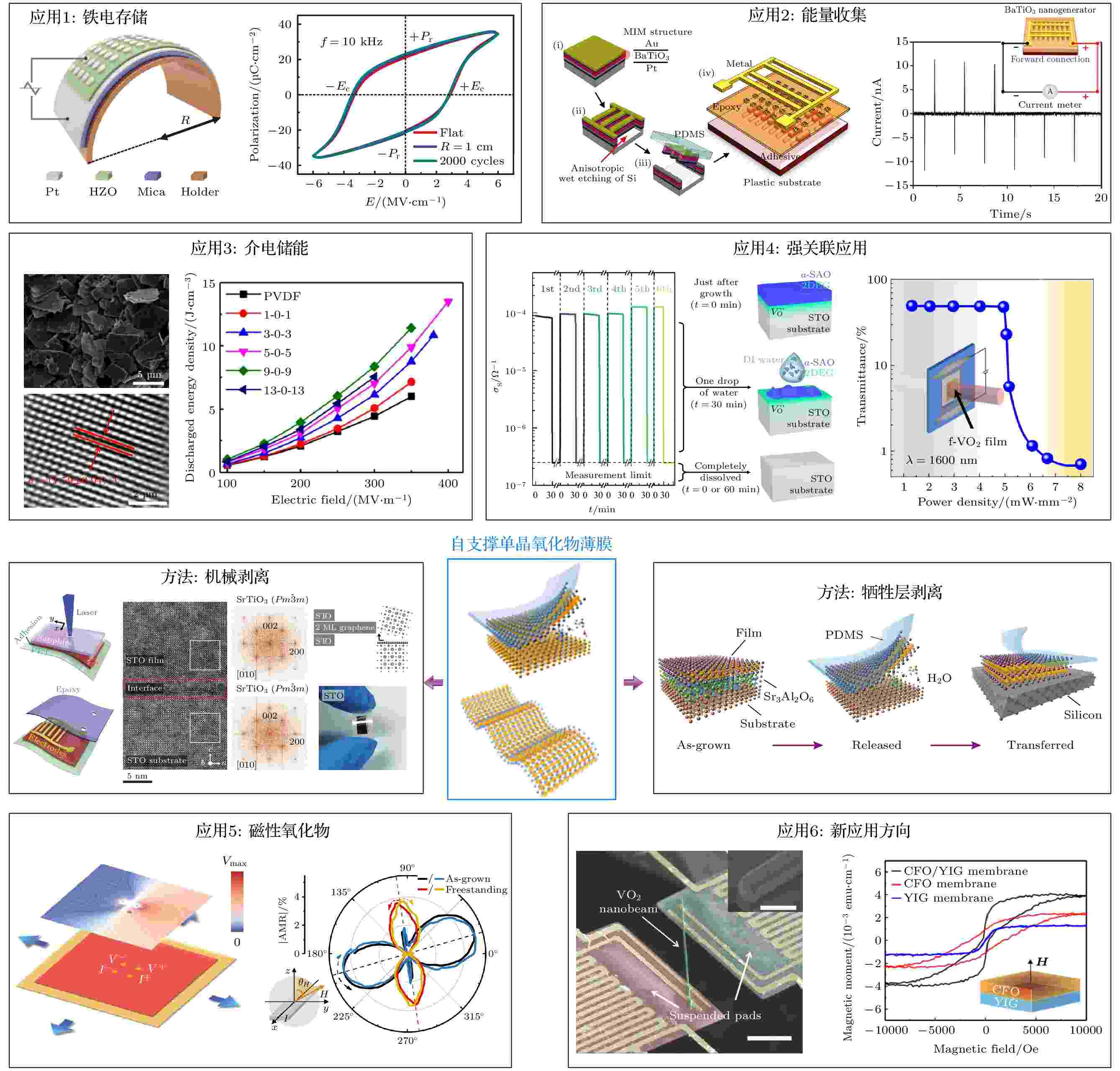
Flexible electronics have aroused great interest of researchers because of their wide applications in information storage, energy harvesting and wearable device. To realize extraordinary functionalities, freestanding single crystal oxide thin film is utilized due to its super elasticity, easy-to-transfer, and outstanding ferro/electric/magnetic properties. Using the state-of-art synthesis methods, functional oxide films of various materials can be obtained in freestanding phase, which eliminates the restrictions from growth substrate and is transferable to other flexible layers. In this work, we first introduce wet etching and mechanical exfoliation methods to prepare freestanding single crystal oxide thin film, then review their applications in ferroelectric memory, piezoelectric energy harvester, dielectric energy storage, correlated oxide interface, and novel freestanding oxide structure. The recent research progress and future outlooks are finally discussed.
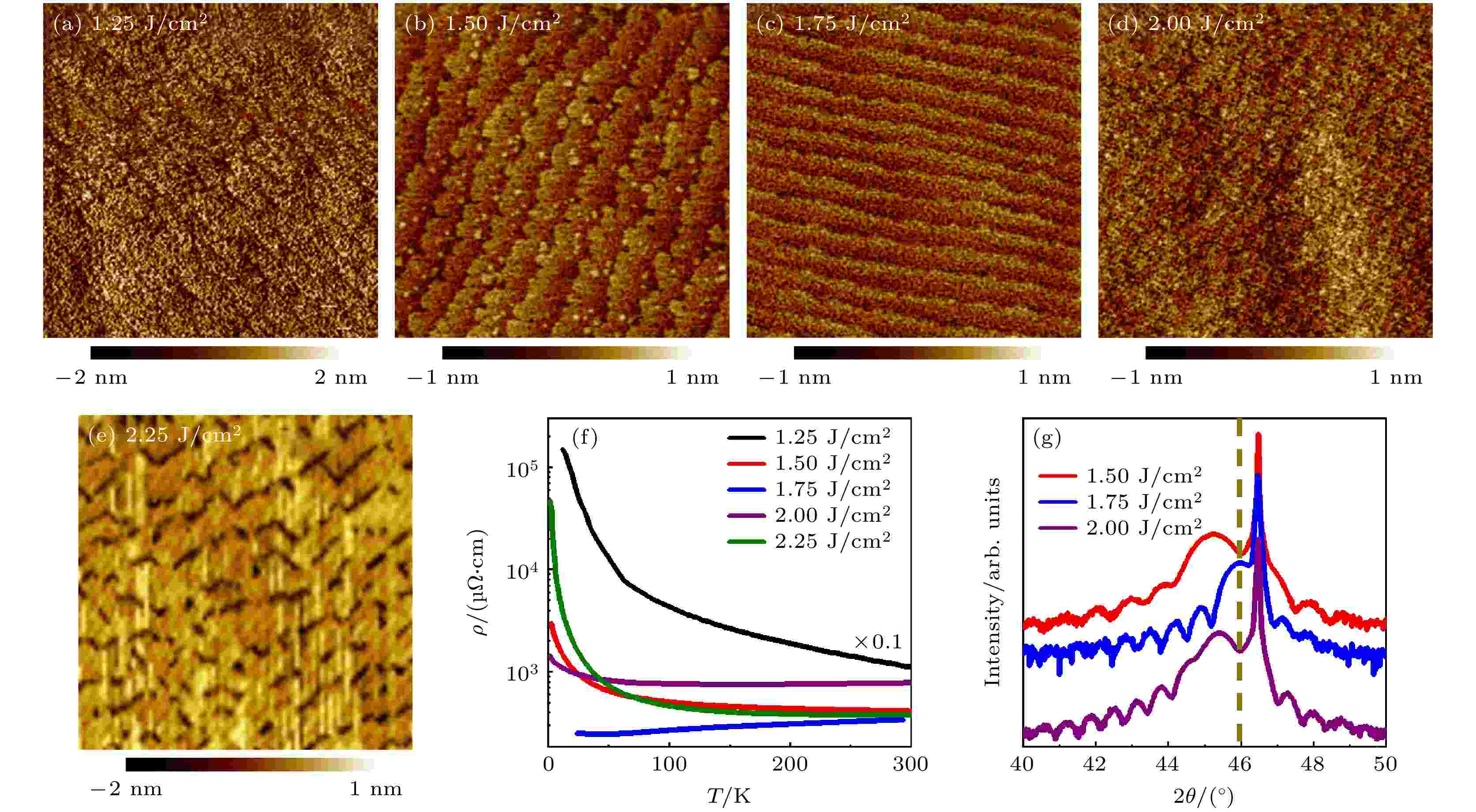
2023, 72 (9): 096802.
doi: 10.7498/aps.72.20221854
Abstract +
As one of the magnetic transition metal oxides, SrRuO3 (SRO) has received much attention in recent years, which is mainly due to its unique itinerate ferromagnetism and the unusual electrical transport properties–behaving as Fermi liquid at low temperature and bad metal at high temperature. In the growth of SRO thin films, there are many factors that can affect the quality of thin films. In this work, we study various factors affecting the growth and quality of SRO thin films by using laser molecular beam epitaxy (laser MBE), including laser energy density, substrate temperature and target surface conditions, and explore their influences on the topological Hall effect (THE) in SRO. For thin films grown at high laser energy density and high temperature, we found that there are large trenches at the edge of steps, which deteriorate the transport properties of the thin films. When using low laser energy density, extra SrO may exist in the films, which also suppresses the conductivity. Films grown at low temperature tend to have poor crystallinity while films grown at high temperature exhibit island structures. The ablation degree of the target surface increases the decomposition of SRO to SrO, Ru and volatile RuO4, resulting in Ru defects in the grown thin film. The SRO thin film grown under the optimal conditions (1.75 J·cm–2, 670 ℃, fresh target surface) exhibits the optimal conductivity and the strongest THE. For non-optimal growth conditions that favors thickness inhomogeneity or Ru defects in the film, THE becomes weaker or even disappears. Therefore, we believe that the THE is due to the Dzyaloshinskii-Moriya interaction (DMI) resulting from the interfacial inversion asymmetry and the associated chiral spin structures.

2023, 72 (9): 096803.
doi: 10.7498/aps.72.20222301
Abstract +
The development of high-performance thermoelectric materials can help solve the energy crisis in the future. Thin-film thermoelectric materials can meet the requirement for flexibility of wearable devices while supplying electrical power to them. In this study, high-quality Nb-doped SrTiO3 films (Nb:STO) with different thickness are prepared on SrTiO3 (STO) and La0.3Sr0.7Al0.65Ta0.35O3 (LSAT) substrates by pulsed laser deposition. The surface morphologies, crystal structures, and thermoelectric performances of the films are characterized. The results show that the thermoelectric performance of the strain-free film increase with thickness increasing. The power factor at room temperature increases by 187%. The Seebeck coefficient of the 144 nm-thick Nb:STO/LSAT sample with strain is greatly improved to $265.95\;{\text{μ}}{\rm{V}}/{\rm{K}}$ at room temperature, which is likely to be due to the strain induced changes in the energy band of the thin film. The improvement of the thermoelectric performances of Nb:STO thin films by strain engineering provides a new approach to improving the thermoelectric properties of oxide thin films.

COVER ARTICLE
2023, 72 (9): 097301.
doi: 10.7498/aps.72.20221934
Abstract +
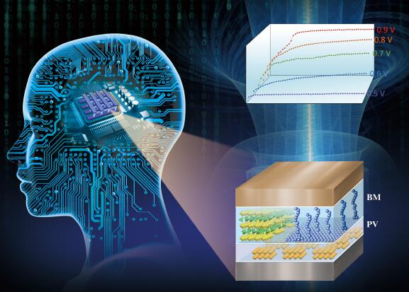
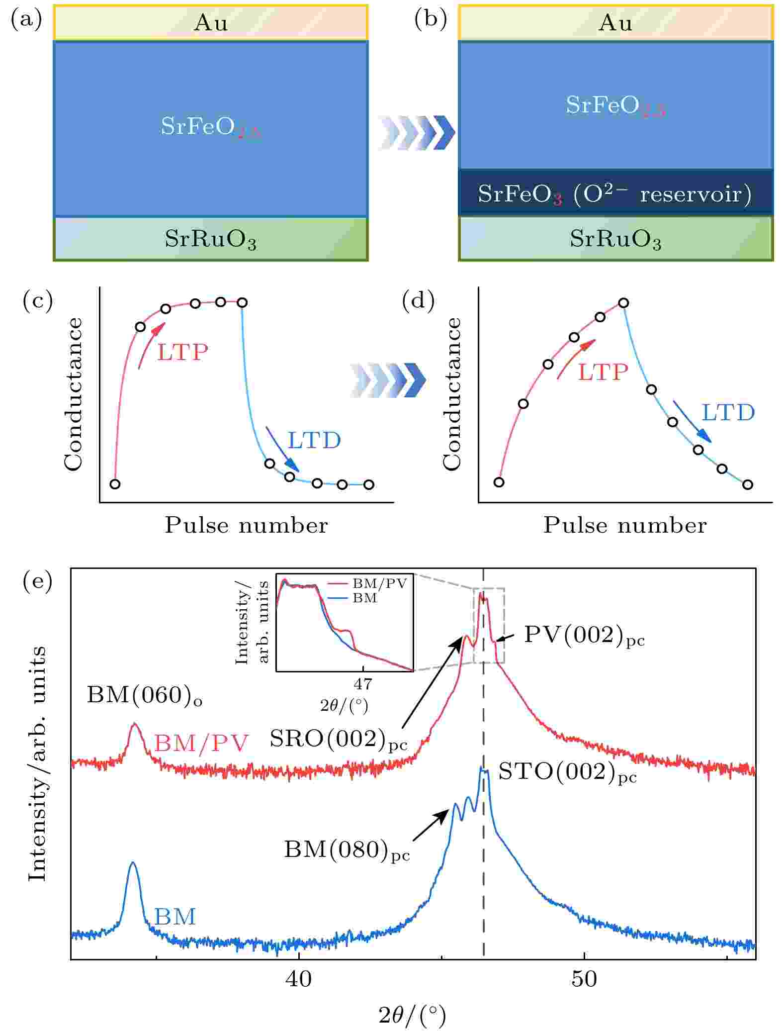
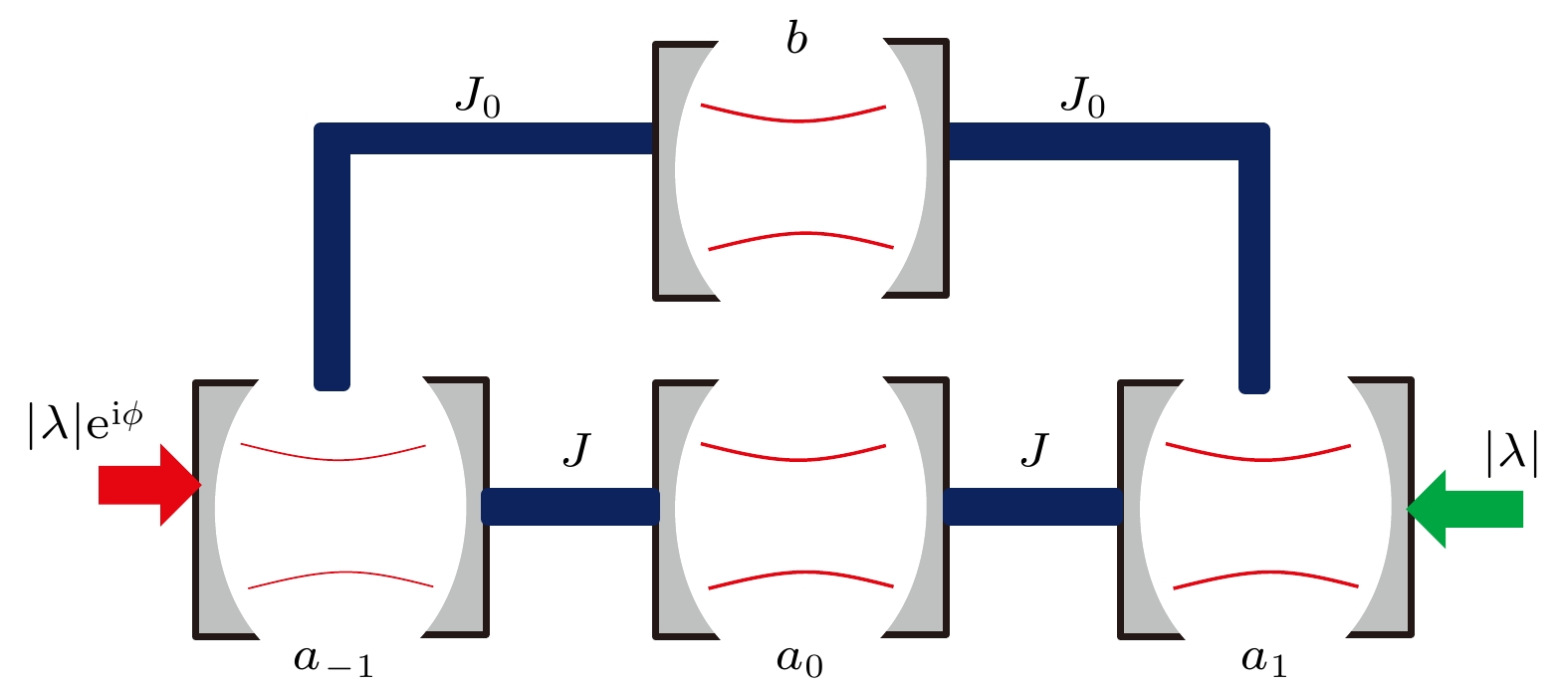
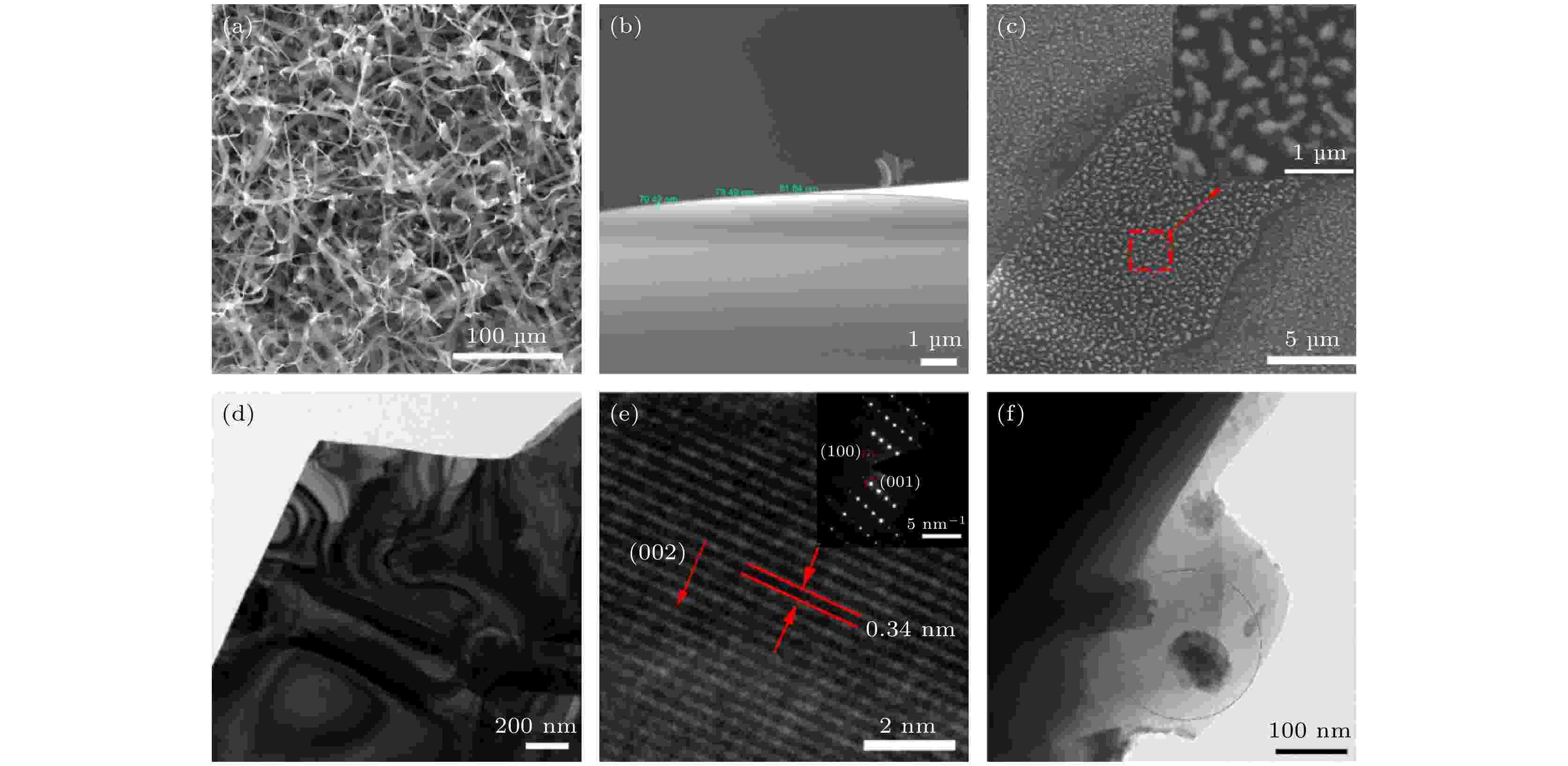
SrFeOx (SFO) is a kind of material that can undergo a reversible topotactic phase transformation between an SrFeO2.5 brownmillerite (BM) phase and an SrFeO3 perovskite (PV) phase. This phase transformation can cause drastic changes in physical properties such as electrical conductivity, while maintaining the lattice framework. This makes SFO a stable and reliable resistive switching (RS) material, which has many applications in fields like RS memory, logic operation and neuromorphic computing. Currently, in most of SFO-based memristors, a single BM-SFO layer is used as an RS functional layer, and the working principle is the electric field-induced formation and rupture of PV-SFO conductive filaments (CFs) in the BM-SFO matrix. Such devices typically exhibit abrupt RS behavior, i.e. an abrupt switching between high resistance state and low resistance state. Therefore, the application of these devices is limited to the binary information storage. For the emerging applications like neuromorphic computing, the BM-SFO single-layer memristors still face problems such as a small number of resistance states, large resistance fluctuation, and high nonlinearity under pulse writing. To solve these problems, a BM-SFO/PV-SFO double-layer memristor is designed in this work, in which the PV-SFO layer is an oxygen-rich interfacial intercalated layer, which can provide a large number of oxygen ions during the formation of CFs and withdraw these oxygen ions during the rupture of CFs. This allows the geometric size (e.g., diameter) of the CFs to be adjusted in a wide range, which is beneficial to obtaining continuously tunable, multiple resistance states. The RS behavior of the designed double-layer memristor is studied experimentally. Compared with the single-layer memristor, it exhibits good RS repeatability, small resistance fluctuation, small and narrowly distributed switching voltages. In addition, the double-layer memristor exhibits stable and gradual RS behavior, and hence it is used to emulate synaptic behaviors such as long-term potentiation and depression. A fully connected neural network (ANN) based on the double-layer memristor is simulated, and a recognition accuracy of 86.3% is obtained after online training on the ORHD dataset. Comparing with a single-layer memristor-based ANN, the recognition accuracy of the double-layer memristor-based one is improved by 69.3%. This study provides a new approach to modulating the performance of SFO-based memristors and demonstrates their great potential as artificial synaptic devices to be used in neuromorphic computing.
2023, 72 (9): 097302.
doi: 10.7498/aps.72.20222222
Abstract +
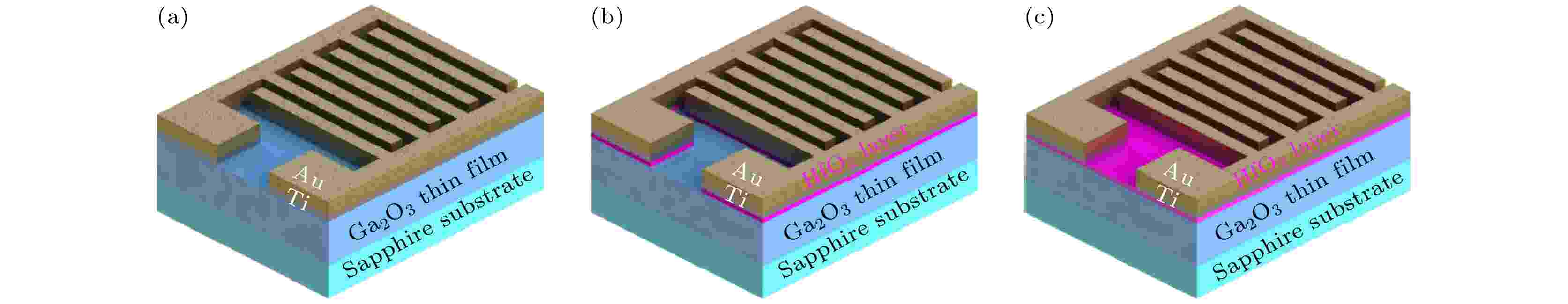
Solar-blind photodetector (PD) converts 200–280 nm ultraviolet (UV) light into electrical signals, thereby expanding application range from security communication to missile or fire alarms detections. As an emerging ultra-wide bandgap semiconductor, gallium oxide (Ga2O3) has sprung to the forefront of solar blind detection activity due to its key attributes, including suitable optical bandgap, convenient growth procedure, highly temperture/chemical/radiation tolerance, and thus becoming a promising candidate to break the current bottleneck of photomultiplier tubes. The Ga2O3-based solar blind PDs based on various architectures have been realized in the past decade, including photoconductive PDs, Schottky barrier PDs, and avalanche PDs. Till now, the metal-semiconductor-metal (MSM) structure has been widely used in developing photoconductive Ga2O3 solar-blind PDs because of its simple preparation method and large light collection area. Unfortunately, despite unremitting efforts, the performance metric of reported MSM-type Ga2O3 solar-blind PDs still lags behind the benchmark of commercial PMTs. Apparently, lack of solution to the problem has greatly hindered further research and practical applications in this field. One effective strategy for further enhancing the device performance such as detectivity, external quantum efficiency (EQE), and light-to-dark ratio heavily relies on blocking the dark current. In this work, high-quality single crystalline β-Ga2O3 with a uniform thickness of 700 nm is grown by using a metal organic chemical vapor deposition (MOCVD) technique. Then atomic layer deposition (ALD) fabricated ultrathin hafnium oxide (HfO2) films ( $ \sim $ 10 nm) are introduced as inserted insulators and passivation layers. The 30 nm/100 nm Ti/Au interdigital electrodes (length: 2800 μm, width: 200 μm, spacing: 200 μm, 4 pairs) are fabricated by sputtering on the top of the film as the Ohmic contacts. Taking advantage of its novel dielectric and insulating properties, the leakage current on Ga2O3 thin film can be effectively inhibited by the inserted ultrathin HfO2 layer, and thus further improving the performance of PDs. Compared with simple MSM structured Ga2O3 PD, the resulting metal-insulator-semiconductor (MIS) device significantly reduces dark current, and thus improving specific detectivity, enhancing light-to-dark current ratio, and increasing response speed. These findings advance a significant step toward the suppressing of dark current in MSM structured photoconductive PDs and provide great opportunities for developing high-performance weak UV signal sensing in the future.


2023, 72 (9): 097503.
doi: 10.7498/aps.72.20221852
Abstract +
Many emergent and novel phenomena occur in nonmagnetic/ferromagnet heterostructures. In particular, Pt/ferromagnet heterostructures where the Pt has strong spin-orbit coupling and thus can convert spin current into charge current, has attracted a great attention recently. The anomalous Hall effect (AHE) has been found in many Pt/ferromagnet heterostructures. However, the underlying physics remains elusive, so it is necessary to find more heterostructures in order to provide more experimental data. In this work, we investigate anomalous Hall resistances (AHRs) in Pt thin films sputtered on epitaxial La0.67Sr0.33MnO3 (LSMO) ferromagnetic films. High-quality Pt/LSMO heterojunctions are fabricated by pulsed laser deposition and RF-magnetron sputtering. The physical properties of LSMO films are characterized by the measurements of magnetic and transport properties. The AHR mainly contributed by Pt in the Pt/LSMO heterojunction increases sharply with temperature decreasing and changes its sign below 40 K. Furthermore, the AHR decreases sharply with the increase of Pt thickness. Those facts suggest that the ferromagnetism of Pt originates from interface due to magnetic proximity effect. Interestingly, this heterojunction can exhibit possible signal of topological Hall effect under low applied magnetic field. The above results provide an experimental basis for further understanding the interactions between electron spin and charge transport in nonmagnetic/ferromagnetic heterostructures.
Composition-spread epitaxial ferroelectric thin films for temperature-insensitive functional devices
2023, 72 (9): 097701.
doi: 10.7498/aps.72.20230154
Abstract +
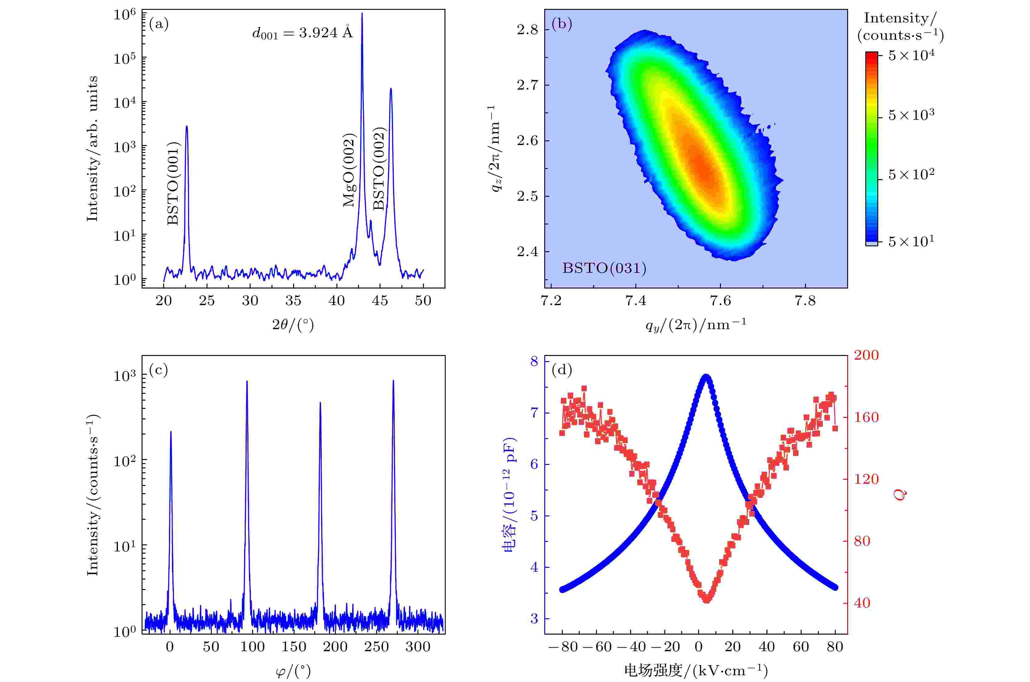
BaxSr1–xTiO3 (BST) ferroelectric thin films are widely used in microwave tunable devices due to their high dielectric constants, strong electric field tunabilities and low microwave losses. However, because of the temperature dependence of dielectric constant in ferroelectric material, the high-tunability for conventional single component ferroelectric thin film can only be achieved in the vicinity of Curie Temperature (TC) which leads the ferroelectric thin films to be difficult to operate in a wide temperature range. To obtain ferroelectric thin films for temperature stable functional devices, single composition Ba0.2Sr0.8TiO3 thin films, Ba0.5Sr0.5TiO3 thin films, and Ba0.2Sr0.8TiO3/Ba0.5Sr0.5TiO3 heterostructure thin films are deposited by pulsed laser deposition (PLD). By comparing their dielectric properties in a wide temperature range, it is found that the temperature sensitivity of BST film can be effectively reduced by introducing a composition gradient along the epitaxial direction. However, the heterostructure engineering may bring extra troubles caused by interfaces, which may limit the quality factor Q. In this paper, we extend our combinatorial film deposition technique to ferroelectric materials, and we successfully fabricate in-plane composition-spread Ba1–xSrxTiO3 thin films, which are expected to broaden the phase transition temperature ranges of BST films while avoiding the problem of interface control.
ATOMIC AND MOLECULAR PHYSICS

2023, 72 (9): 093201.
doi: 10.7498/aps.72.20230261
Abstract +
Laser heterodyne radiometer has the advantages of low cost, small size, and high spectral resolution. It can expand the existing ground carbon measurement network, verify satellite observation results, and provide data coverage outside the satellite observation area. Using the existing laser heterodyne radiometer, is presented a prototype of near-infrared laser heterodyne radiometer based on the erbium-doped fiber amplifier that can realize local oscillator power locking. In the laser heterodyne radiometer a distributed feedback semiconductor laser with a center wavelength of 1.603 μm is used as a local oscillator light source. The erbium-doped fiber amplifier is used to enhance the local oscillator power, and the automatic power control circuit is adopted to lock the output optical power of the erbium-doped fiber amplifier. The baseline slope caused by the change of the local oscillator power is eliminated, and the whole layer atmospheric transmittance spectrum without baseline fitting is measured. The instrument performance of a highly integrated laser heterodyne radiometer based on an erbium-doped fiber amplifier is evaluated in detail, and the atmospheric CO2 transmittance spectrum is measured in the Science Island (31.9°N, 117.2°E) of Hefei. Six groups of atmospheric CO2 transmittance spectra are obtained during the measurement period of one day, which are compared with the simulation results from an atmospheric radiation model, showing that they are consistent with each other. The experimental results show that the application of erbium-doped fiber amplifier can improve the performance of laser heterodyne radiometer, optimize its structure, and provide equipment supplement for realizing unattended long-term atmospheric CO2 concentration observation and building a comprehensive carbon observation network.

2023, 72 (9): 093401.
doi: 10.7498/aps.72.20222273
Abstract +
The time-of-flight mass spectrum of charged particles, which are created through two-step cw-laser photoionization of laser-cooled 87Rb atoms in an ion-neutral hybrid trap, is quantitatively investigated to further facilitate the study of Rb+-Rb reactive collisions. A microchannel plate (MCP) is used to detect charged particles, and two spectral peaks corresponding to the 87Rb+ ions and the product $ \rm {}^{87}Rb_2^+ $ of the Rb+-Rb reaction were observed in the time-of-flight spectrum, respectively. The two peaks overlapped with each other and both showed an asymmetric profile. The information about the intensity, position, and half-width of the peak for a specific ion species was derived by fitting the time-of-flight spectrum with the probability density function of the Gumbel distribution. Then the relative ion intensity was converted into absolute ion number through the following steps. The rate equation of the total number of ions, which includes the number of atoms, the calibration factor of MCP, and the effective decay rate of ions in the ion trap, was established by modeling the photoionization of atoms. Combined with the absolute number of atoms measured by absorption imaging, the calibration factor in converting the ion intensity into the ion number was derived and the relative ion intensity was converted into the absolute number of ions. This provides a method of calibrating the MCP. The reliability of our calibration method was proved by the fact that the calibration factor in converting the intensity measured by MCP into particle number is independent of the duration of photoionization, the intensity and wavelength of the ionizing laser. Moreover, in order to explain the relationship between the peak width and temperature of the corresponding ion species, the time-of-flight spectra of the ions trapped in the ion trap were simulated by using COMSOL Multiphysics. The simulation results demonstrated that the large ion kinetic energy results in a narrow spectral peak. In sum, we quantitatively analyze and simulate the time-of-flight spectrum of the photoionization of cold atoms in the Rb+-Rb hybrid trap. The absolute number of ions is obtained by the intensity of the spectral peak, and the width of the spectral peak is related to the temperature of the ions. These results lay a foundation for the in-depth analysis of the ion-atom reaction collision and charged particle temperature relaxation in the photoionization of cold atoms, and thus further elucidating the subsequent collisional dynamics of ultracold plasmas.

ELECTROMAGNETISM, OPTICS, ACOUSTICS, HEAT TRANSFER, CLASSICAL MECHANICS, AND FLUID DYNAMICS

2023, 72 (9): 094201.
doi: 10.7498/aps.72.20221560
Abstract +
The electromagnetically induced transparency (EIT) effect is a quantum coherence effect between different atomic transition channels. The absorption of the atomic ensemble is significantly reduced or even close to zero, and at the same time, this effect is accompanied by strong spectral dispersion near the resonant frequency of atoms, which is widely used in group velocity control, light pulse storage, and coherent manipulation on the light field. In the light pulse storage based on the EIT effect, the retrieval field is determined by the signal, coupling, and readout fields, enabling the retrieval field to be dynamically controlled by manipulating the spatial frequency components of the interacting light fields. In this paper, according to the EIT effect, we achieve experimentally the optical image addition and subtraction in the imaging plane of a 4$f$ system through the coherent manipulation of the retrieval field via the interacting signal, coupling, and readout fields. Specifically, we first store the spatial frequency spectrum of a double-slit mask in the praseodymium-doped yttrium silicate crystal located in the confocal plane of the 4$f$ system based on the EIT effect. Then, we utilize a specially designed mask containing the target objects and perform spatial filtering by using the spatial frequency spectrum of the double-slit mask through the retrieval of stored light pulse. By moving the double-slit mask, the addition and subtraction between the images of target objects can be achieved in the imaging plane of the 4$f$ system. We present a theoretical model to describe the addition and subtraction between the target images through the EIT-based light pulse storage technique. The experimental results accord well with the theoretical prediction. Compared with the traditional scheme with a cosine grating filtering the spatial frequency spectrum, our method does not require the preparation of a spatial frequency filter, and only produces the first-order positive and negative diffraction images without the influence of the zeroth-order diffraction image. The optical image addition and subtraction based on the EIT effect provide a new approach to optical image processing. This approach is not limited to image addition or subtraction, and it can be extended to achieve more complex operations such as differentiation, enhancement, encryption, and decryption with rational design. Therefore, it can be widely used in areas such as coherent manipulation of light fields and dynamic optical image processing.

2023, 72 (9): 094202.
doi: 10.7498/aps.72.20230049
Abstract +


2023, 72 (9): 094203.
doi: 10.7498/aps.72.20222264
Abstract +
Rydberg atoms have attracted considerable attention due to their several singular properties, such as strong long-range interactions, extremely long lifetimes, and very large polarizability. These characteristics make Rydberg atoms a good candidates for cavity quantum electrodynamics, quantum information, and many-body physics. Recently, the study of optomechanics has become a rapidly developing field due to its important applications in cooling of mechanical resonators, implementing precision measurements, slowing light, and preparing quantum entanglement. Obviously, optomechanical systems pave the way for quantum information processing and quantum communication. Specially, there is significant interest in quantum optomechanics due to its high compatibility that can be combined, to build hybrid systems for certain purposes, with the ultracold atoms, a superconducting single electron transistor, a magnetostrictive actuation, a charged oscillator resonator, etc. In this work, we investigate the optomechanically induced transparency (OMIT) and the resulting effect of slow light in a hybrid system composed of a Rydberg atomic ensemble embedded inside a simple optomechanical cavity. As a typical effect of destructive quantum interference, OMIT is widely used in quantum optics and quantum information processing. Based on the Rydberg blockade effect, a Rydberg atomic ensemble in the same blockade region embedded inside an optomechanical cavity can be regarded as a superatom that contains only a single Rydberg excitation. Therefore, the problem of exponentially increasing system size with the number of atoms increasing can be circumvented easily. The hybrid system becomes a coupling between a Rydberg superatom and an optomechanical cavity and the coupling strength is enhanced by a factor of square root of the number of atoms in the ensemble. In this system, the perfect OMIT, namely, an ideal OMIT dip with a very narrow window, can be attained when an effect of non-rotating wave approximation (NRWA) is considered. Further, we demonstrate that the term of NRWA plays a key important role in achieving perfect OMIT by comparing the optomechanical spectra obtained with and without NRWA effects. Our results show that in the resolved sideband regime the higher the quality factor of cavity is, the stronger the slow light effect becomes in the window of the perfect OMIT. Particularly, in achieving the ultraslow light, the long lifetime of the Rydberg atom shows its superiority.

2023, 72 (9): 094204.
doi: 10.7498/aps.72.20222387
Abstract +
The development of optical parametric chirp pulse amplification (OPCPA) numerical simulation platform involves physical models such as broadening and compression of optical pulse, parametric amplification and focusing output. In the simulation platform, the Fresnel far-field diffraction equation is usually used to simulate the characteristics of ultrashort pulse focusing. Firstly, we need to calculate the optical field distribution of different wavelength components in the ultrashort pulse, and then use the inverse Fourier transform to obtain the temporal and spatial distribution characteristics of the pulse. However, for different wavelength components, the sizes of focused field grids obtained by the far-field algorithm are not equal, and subsequent resampling is required, which will increase the amount of calculation. In addition, due to the limitation of the calculation range of the light field in the pulse broadening and compression, there is also a problem of poor resolution of the focused field. In this work, the mathematical expression that can adjust the range of the output light field and use the fast fourier algorithm is derived. The main mechanism of this algorithm is as follows. Based on the Fresnel far-field diffraction equation, the output field is sampled independently in the discrete calculation process to meet the requirements for adjustable range of the output field. After identity transformation, the output field results can be calculated by the fast Fourier algorithm. Furthermore, the sampling conditions that need to be satisfied when using the algorithm are further analyzed and discussed. It solves the problem of how to improve the resolution of light field and keep the computational grid size of each wavelength component consistent when the traditional Fresnel far field diffraction is used to simulate the focusing process, which provides the convenience for the subsequent direct time-frequency inverse transformation. The numerical simulation results reveal that the dark ring region of the ultrashort pulse focusing field shows strong spatiotemporal coupling characteristics. This algorithm has been successfully applied to the development of OPCPA numerical simulation platform, and is expected to play an important role in optimizing the design of ultrashort laser pulse device.

2023, 72 (9): 094205.
doi: 10.7498/aps.72.20230088
Abstract +
Self-phase modulation-enabled spectral selection (SESS) technology can generate wavelength-tunable femtosecond pulses, and it is expected to replace traditional complex optical parametric oscillators, and thus has attracted much attention. However, the positive dispersion in the fiber leads the modulation depth of the spectral lobes to decrease, while optical wave breaking hinders the spectral broadening. In order to solve the two problems, we propose a dual-pass SESS technology based on dispersion management which optimizes the shape of the front edge and rear edge of the pulse prior to the second pass by introducing negative dispersion, and compresses the pulse width for increasing the peak power of the pulse. The resulting spectrum features broader spectrum with a deeper modulation depth. By numerical simulation, we find that adjusting the value of the second-order dispersion compensated after the single pass, a broader spectral lobe can be obtained than both the single-pass case and the double-pass case without dispersion compensation. To verify our numerical simulation, we conduct experiments by using a 2-cm-long LMA-8 fiber for spectral broadening and several chirped mirrors to provide negative dispersion, which controls the nonlinear evolution of the pulse in the second pass of the LMA-8 fiber. We study the spectral output corresponding to different amounts of dispersion compensation and find that an optimal dispersion value is required to produce a clear and broader spectral lobe. We also investigate the effect of input pulse energy on spectral broadening under the same dispersion compensation conditions. With 15-nJ input pulse energy and –420 fs2 dispersion compensation, the resulting SESS source delivers 6 nJ, 113-fs pulses with the peak wavelength at 920 nm.

2023, 72 (9): 094301.
doi: 10.7498/aps.72.20230195
Abstract +
PHYSICS OF GASES, PLASMAS, AND ELECTRIC DISCHARGES
2023, 72 (9): 095201.
doi: 10.7498/aps.72.20222005
Abstract +
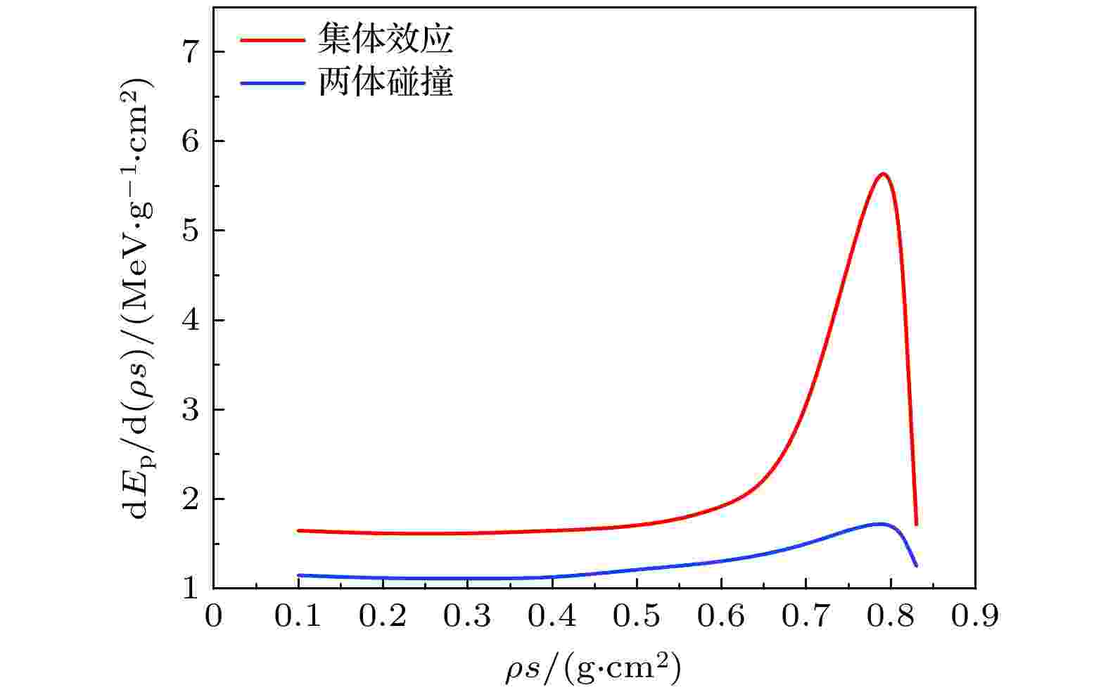
The proton beam energy deposition and the prodution of proton beams in proton fast ignition are investigated with the fluid program, partice-in-cell program and Fokker-Planck program based on the parameters of Shenguang II upgraded device. Firstly, according to the target parameters of fast ignition, the energy depositions of different energy protons are investigated. It is obtained that the higher the incident proton energy, the higher the surface density that the protons go through, accordingly the longer the proton deposition distance in the same background plasma density. On the assumption that the diameter of the compression core is 20–30 μm, and that the protons deposited in the core give the energy to the background plasma, the energy of the proton required by fast ignition is obtained by Fokker-Planck simulation. Protons with energy of 7–12 MeV are appropriate for ignition when the background plasma density is 300 g/cm3, while 8–18 MeV protons for 400 g/cm3. The background plasma temperatures are both 5 keV in the two cases. Secondly, we use particle-in-cell program to study the proton acceleration with or without preplasma which is given by fluid program with using the laser intensity $ I = 5.4 \times {10^{19}}{\text{ }}{\rm{W/c}}{{\rm{m}}^2} $ based on the parameters of Shenguang II upgraded device. The laser has 350 J of enegy, 3 ps of Gaussion pluse width and 10 µm of spot radius. The curvature of the target which is 10 µm thick copper coated with 1 µm thick hydrogen plasma, is 500 µm. The maximum proton energy obtained with preplama is 22 MeV, however the maximum proton energy obtained without preplasma is 17.5 MeV. The conversion efficiency from laser to protons is 5.12% with preplasma and 4.15% without preplasma. The conversion efficiency with preplasma is 20% higher than that without preplasma. We also study the mechanisms of the acceleration in the two situations. The freely expanding plasma model is used to explain the acceleration mechanism. The simulated electric field is smaller than that calculated by using the freely expanding plasma model, because some protons are accelerated at the time of plasma expansion, which consumes some electric field. The results of proton energy deposition show that the proton beams that are suitable for fast ignition can be obtained by the Shenguang II upgraded device.


2023, 72 (9): 095202.
doi: 10.7498/aps.72.20222235
Abstract +
The secondary electron multipactor on the inner surface of the output window is one of the main factors limiting the power capacity of high power microwave. Therefore, it is of great significance to carry out relevant research. In this work, the process of secondary electron multipactor and the resulting loss of power are numerically simulated by using the electromagnetic particle model with one-dimensional spatial distribution and three-dimensional velocity distribution at the microwave frequency of 110 GHz. The influences of microwave electric field at the surface and dielectric material type on the power loss are studied. The simulation results show that the electron number density is higher than the critical cut-off number density after the secondary electron multipactor has reached the steady state, but the microwave electric field does not show obvious change. This is because the electrons in a very high electrostatic field are mainly concentrated in the domain of several micrometers near the dielectric surface, which is far less than the corresponding skin depth. The electron number density in the multipactor steady state increases with the microwave electric field increasing, but the ratio of the power loss to the microwave power at the surface increases slowly. After the multipactor reaches the steady state, the number density of electrons near the sapphire surface is the highest, followed by the number density near the crystal quartz surface, and the number density near the fused quartz surface is the lowest, so the corresponding power loss decreases successively. In order to verify the accuracy of the model, the simulated value of the multipactor threshold is compared with the experimental data, and the difference between them is discussed.
CONDENSED MATTER: STRUCTURAL, MECHANICAL, AND THERMAL PROPERTIES
2023, 72 (9): 096201.
doi: 10.7498/aps.72.20221615
Abstract +
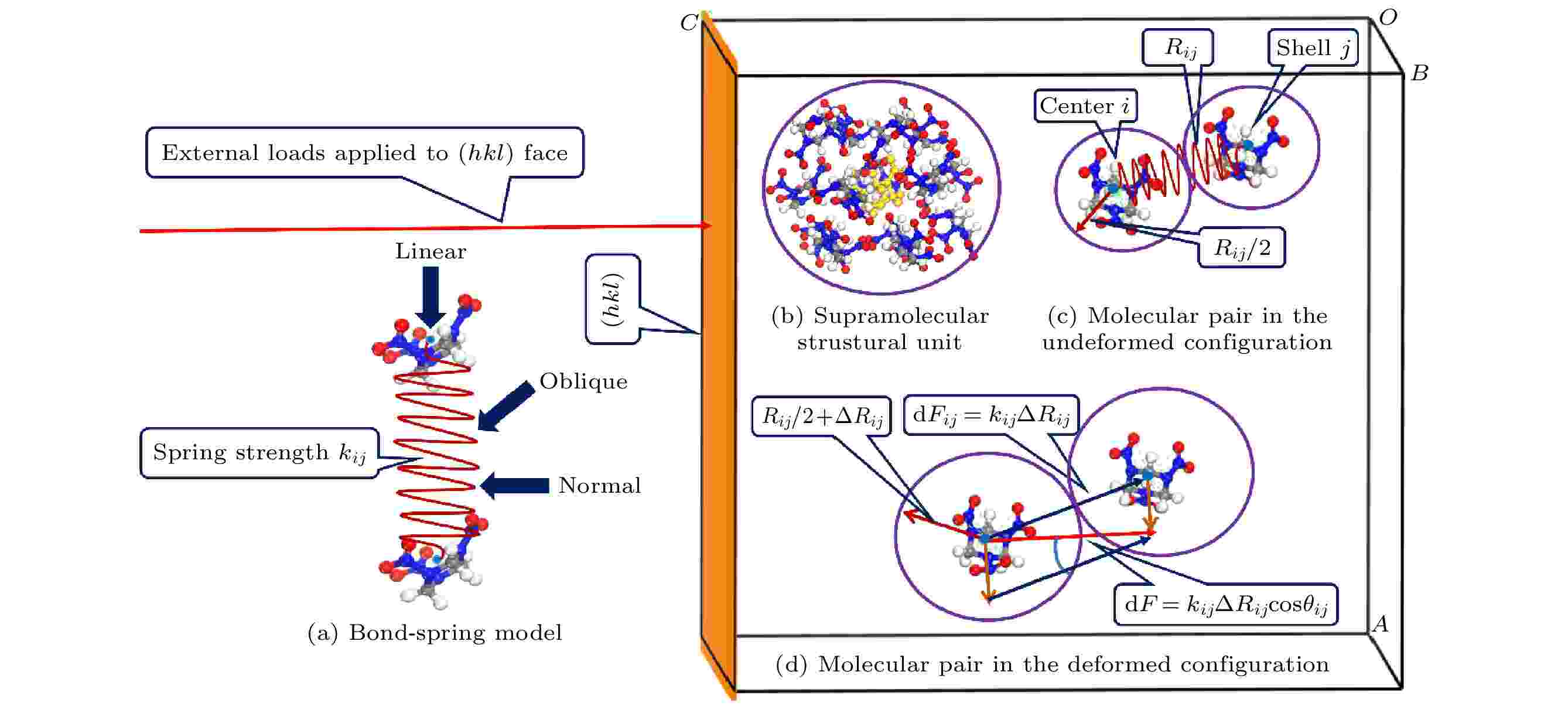
The relation between elastic property and crystal structure provides a foundation for designing new materials with desired properties and understanding the chemical decomposition and explosion of energetic materials. The supramolecular structural unit is proposed as the smallest chemical unit to quantitatively characterize the elastic anisotropy of 1, 3, 5-trinitro-1, 3, 5-triazacyclohexane (RDX). The supramolecular structural unit refers to the nearest-neighbor coordination polyhedron of one molecule. The supramolecular structural unit of RDX is composed of 15 molecules, and analyzed by the total molecular number density and the density of intermolecular interactions. The elastic modulus model is established on the assumption that 1) the RDX molecule is of sphere and rigid-body; 2) the intermolecular interaction is regarded as a linear spring, i.e. it is described by a bond-spring model; 3) the molecules are close-packed in the series mode. The elastic modulus model based on the supramolecular structural unit demonstrates that the elastic modulus is intrinsically determined by the total molecular number, the equilibrium distance of the molecular pair, the intermolecular force constant, and the angle between the intermolecular non-bonding interaction and the normal to crystal face. The intermolecular force constant is calculated as the second derivative of the intermolecular interaction with respect to the equilibrium centroid distance. The intermolecular interaction is expressed as the summation of van der Waals and electrostatic interactions calculated by COMPASS (condensed-phase optimized molecular potentials for atomistic simulation studies) II forcefield. The calculated elastic moduli are 21.7, 17.1, 20.1, 19.1, and 15.3 GPa for RDX (100), (010), (001), (210), and (021) crystal faces, respectively. The calculation results are consistent with the theoretical values computed by the density functional theory. Excluding RDX(001), the calculated elastic moduli accord with the experimental results measured by the resonant ultrasound spectroscopy (RUS), impulsive stimulated thermal scattering, Brillouin spectroscopy, and nanoindentation methods. The theoretical value (20.1 GPa) of RDX(001) overestimates the experimental values in a range of 15.9–16.6 GPa. The reason can be attributed to the rigid-body approximation for flexible molecules, in which are ignored the motion and deformation of the ring and NO2 groups when the external loads are applied to RDX(001). The results suggest that the supramolecular structural unit can be the smallest chemical unit to quantitatively characterize the elastic anisotropy of RDX and the elastic anisotropy is mainly due to the angle between the intermolecular interaction and the normal to crystal face.
2023, 72 (9): 096301.
doi: 10.7498/aps.72.20230116
Abstract +
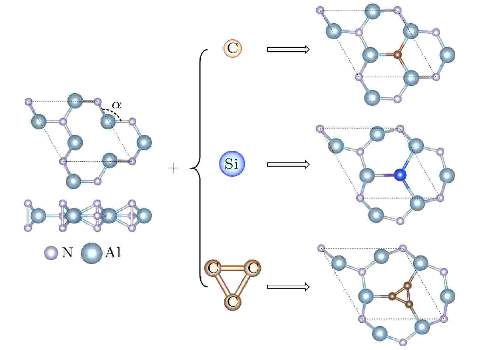
Aluminum nitride (AlN) is of paramount importance in developing electronic devices because of excellent stability and thermal transport performance. However, lack of novel materials which can provide colorful physical and chemical properties seriously hinders further digging out application potential. In this work, we perform an evolutionary structural search based on first-principles calculation and verify the dynamic and thermal dynamic stability of porous buckled AlN and X-AlN (X = C, Si, TC) structural system, which constructs by introducing C, Si atoms and triangular carbon (TC) into the porous vacancy of AlN, by calculating phonon spectra and first-principles molecular dynamic simulations. Structural deformation becomes gradually serious with the increase of structural unit size and significantly influences structural, electronic, and thermal transport properties. Firstly, we point out that a flat energy band appears around the Fermi level in C-AlN and Si-AlN because of weak interatomic interaction between C/Si and the neighbor Al atoms. Unoccupied C-/Si-pz and Al-pz do not form $ {\rm{\pi }} $ bond and only a localized flat band near Fermi level arises, and thus the absorption peaks of structures are enhanced and the red shift occurs. Bonding state of $ {\rm{\pi }} $ bond from hybridized C-pz orbitals in triangular carbon of TC-AlN lowers the energy of conduction band at K point in the first Brillouin zone and the corresponding antibonding state raises the band at Γ, therefore transition from indirect bandgap of AlN to direct bandgap of TC-AlN appears. Secondly, porous buckled AlN shows the lowest thermal conductivity due to asymmetric Al—N bonds around the porous vacancy and vertically stacked N—N bonds. Introduced C and Si atoms both reduce structural anharmonicity, while the former has a relatively small distortion, and so it has a higher thermal conductivity. Triangular carbon in TC-AlN hinders phonon scattering between FA mode and other phonon modes and has the weakest anharmonicity because of the strongest bond strength, and obtains the highest thermal transport performance. Finally, we unveil the physical mechanism of anomalous thermal conductivity in X-AlN system by modulating the biaxial tensile strain. Enhanced vertical N—N bonds dominate thermal transport due to its weaker anharmonicity with a slightly strain, and when tensile strain is above the 4%, soften phonon modes reduce phonon velocity and thus hinders the thermal transport process. Therefore, occurs the anomalous thermal transport behavior, i.e. thermal conductivity first rises and then drops with applied biaxial strain increasing. Our work paves the way for modulating two-dimensional AlN performance and provides a new insight for designing promising novel two-dimensional semiconductors.

CONDENSED MATTER: ELECTRONIC STRUCTURE, ELECTRICAL, MAGNETIC, AND OPTICAL PROPERTIES
EDITOR'S SUGGESTION
2023, 72 (9): 097101.
doi: 10.7498/aps.72.20230231
Abstract +
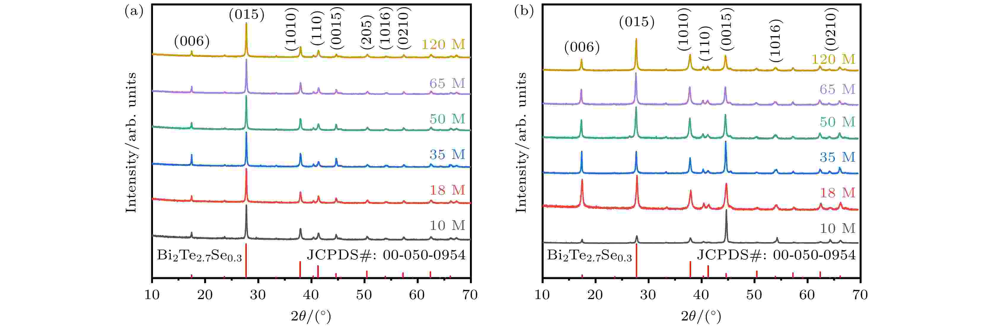
Grain size refinement is the vital stratagem for improving mechanical properties of Bi2Te3-based thermoelectric material. However, the donor-like effect induced by grain size refinement seriously deteriorates the thermoelectric properties especially near room temperature. Once the donor-like effect is generated, it is very difficult to eliminate the donor-like effect by the simple heat treatment process and other processes. In this study, the influences of particle size on the donor-like effect and thermoelectric properties are systematically studied for Bi2Te3-based compounds. As the particle size decreases, the donor-like effect is enhanced significantly. The oxygen-induced donor-like effect dramatically increases the carrier concentration from 3.36× 1019 cm–3 for 10 M sintered sample to 7.33×1019 cm–3 for 120 M sintered sample, which is largely beyond the optimal carrier concentration of 2.51×1019 cm–3 and seriously deteriorates the thermoelectric properties. However, when the particle size of the powder is 1–2 mm, the Seebeck coefficient of –195 μV/K and the carrier concentration of 3.36×1019 cm–3 near room temperature are achieved, which are similar to those of the ZM sample with the Seebeck coefficient of –203 μV/K and the carrier concentration of 2.51×1019 cm–3. The powders without the obvious donor-like effect can be used as the excellent raw material for powder metallurgy process. A maximum ZT value of 0.75 is achieved for the 18 M sintered sample. The excellent thermoelectric properties are expected to be obtained by enhancing the texture further. This study provides a new way to regulate and effectively suppress the generation of the donor-like effect, and provides an important guidance for the preparation of materials with excellent thermoelectric and mechanical properties by powder metallurgy process.
EDITOR'S SUGGESTION
2023, 72 (9): 097501.
doi: 10.7498/aps.72.20230197
Abstract +
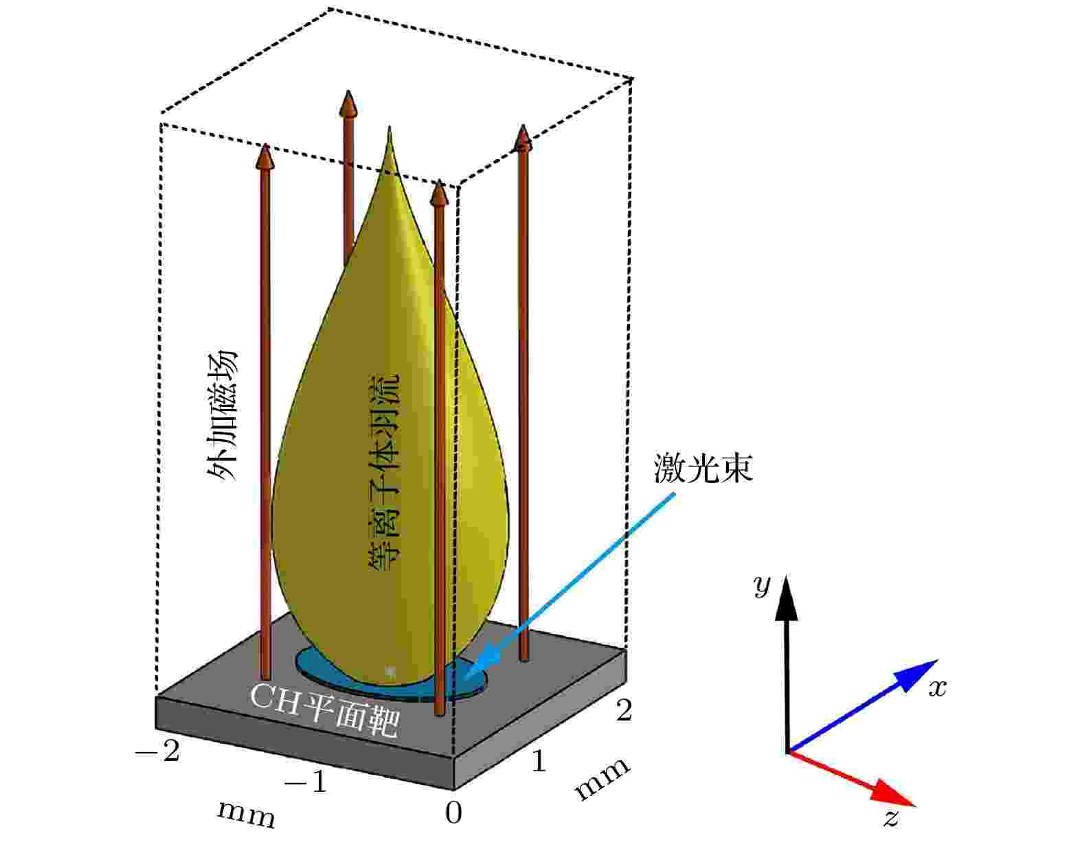
Astrophysical jets are highly collimated supersonic plasma beams distributed across various astrophysical backgrounds. The triggering mechanism, collimation transmission, and stability of jets have always been a research hotspot of astrophysics. In recent years, observations and laboratory research have found that the magnetic field plays a crucial role in jet collimation, transmission, and acceleration. In this work, the two-dimensional numerical simulation of the jet in front of the CH plane target driven by an intense laser is carried out by using the open-source MHD FLASH simulation program. We systematically investigate the dynamic behaviors of jet evolution caused by the Biermann self-generated magnetic field, the external magnetic field with different directions and initial strengths and compare them with each other. Simulation results show that the Biermann self-generated magnetic field does not affect the jet interface dynamics. The external magnetic field has a redirecting effect on the plasma outflow. The external magnetic field, which is parallel to the direction of the plasma outflow center in front of the target, is conducive to the generation and collimation of the jet. The evolution of the jet goes through three stages: antimagnetic ellipsoid cavity, conical nozzle, and collimated jet. Its formation process and evolution process result from competition among plasma thermal, magnetic, and ram pressure. In terms of force, plasma thermal pressure gradient and magnetic pressure forces play a decisive role in the jet evolution process. The presence of magnetic pressure significantly limits the radial expansion of the jet to achieve axial collimation transmission. The length-diameter ratio of the jet is positively correlated with the initial axial applied magnetic field intensity. In addition, we observe in the simulation that there are many node-like structures in the jet evolution zone, similar to the jet node in YSO. The results provide a reference for future experimental research related to jets and contribute to a more in-depth understanding of the evolution of celestial jets.
2023, 72 (9): 097801.
doi: 10.7498/aps.72.20230066
Abstract +
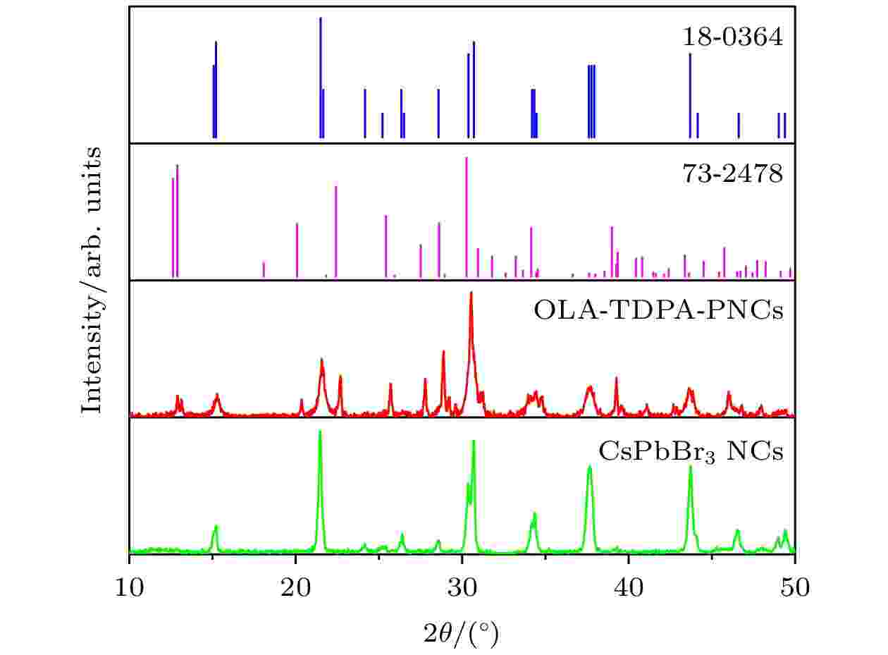
CsPbBr3-Cs4PbBr6 dual-phase nanocrystals are prepared by adding the mixture ligand of oleylamine and tetradecyl-phosphonic acid (OLA-TDPA) to CsPbBr3 perovskite nanocrystals through ligand post-treatment. The structure, the morphology, optical property and the stability of CsPbBr3-Cs4PbBr6 dual-phase nanocrystals are characterized by X-ray diffraction, transmission electron microscopy (high-resolution TEM), UV-vis spectrophotometer, fluorescence spectrophotometer, and transient fluorescence spectrophotometer. The as-obtained nanocrystals have a high photoluminescence quantum yield of 78% and long fluorescence lifetime of 476 ns when prepared at the optimal molar ratio of CsPbBr3, TDPA and OLA (1∶1∶15). Moreover, the nanocrystal is quite stable at room temperature for at least 25 days, and has a good thermal stability in five heating-cooling cycles at temperature in a range between 293 K and 328 K. The formation of dual-phase nanocrystals go through two stages of surface passivation/dissolution and recrystallization to generate CsPbBr3-Cs4PbBr6 nanocrystals. In the first stage (t ≤ 1 h), the m OLA-TDPA mixing ligand can form (RNH3)2PO3 X type ligand and exchanges with [RNH3]+-[RCOO]– at the surface of CsPbBr3 nanocrystals, which can effectively passivate surface defects by strong interaction with Pb2+ and high ligand content at surface, thus improving the quantum yield and fluorescence life of CsPbBr3 nanocrystals with spherical shape. In the second stage, with the increase of reaction time, PbBr2 partially dissolves from the surface of CsPbBr3 nanocrystals, then some CsPbBr3 nanocrystals transform into lead-depleted Cs4PbBr6 nanocrystals with hexagonal phase, thus improving the stability of nanocrystals. This work has a certain reference value for promoting the applications of high efficient and stable perovskite nanocrystals.
INTERDISCIPLINARY PHYSICS AND RELATED AREAS OF SCIENCE AND TECHNOLOGY
2023, 72 (9): 098101.
doi: 10.7498/aps.72.20222321
Abstract +
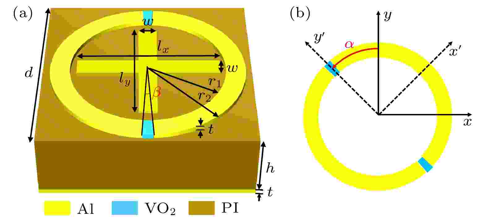
Terahertz (THz) wave has the advantages of low photon energy, high resolution, large communication bandwidth, etc. It has broad application prospects in security detection, high-resolution imaging, high-speed communication, and other fields. In recent years, as a new way to control THz wave, THz metasurface functional devices have attracted extensive attention of researchers. In this work, vanadium dioxide (VO2), a phase change material, is introduced into the coding metasurface. By regulating a circularly polarized wave and the orthogonal linearly polarized waves independently, a multi-function coding metasurface that can work at dual frequency points is obtained. It is composed of three layers. The top layer is a metal-VO2 composite structure. The middle is a polyimide dielectric layer. The bottom is a metal ground. Under certain conditions, the double split ring resonator (DSRR) and the cross structure in the top layer are relatively independent. Designing the coding sequences for them enable the coding metasurface to have multiple functions. The electromagnetic simulation software CST is used to establish model and conduct simulation, and the obtained results are as follows. When the VO2 is in an insulating state and a circularly polarized wave at 0.34 THz is incident vertically, the characteristics of coding metasurface elements are mainly affected by the DSRR. The DSRR is rotated to meet the requirements of 3-bit Pancharatnam-Berry phase coding. The coding sequence is designed to generate vortex beams with the topological charge l = ±1 at a specific angle. The VO2 state is changed into a metallic state, and the DSRR can be equivalent to a metal ring. When the orthogonal linearly polarized wave at 0.74 THz is incident vertically, the characteristics of coding metasurface elements are mainly affected by the cross structure. Because of its anisotropy, four different 2-bit coding metasurface elements can be obtained respectively by changing the length of the horizontal arm and the vertical arm. The design of appropriate coding sequences can reduce the radar cross section of the x-polarized wave and the beam splitting of the y-polarized wave, and the results have broadband characteristics. Multiple coding sequences can be designed by special characteristics of the coding metasurface, then various expected functions can be realized on the same metasurface. It solves the problem of single function of ordinary metasurface devices to a certain extent, and paves a novel way to the development of THz multi-function systems.
2023, 72 (9): 098103.
doi: 10.7498/aps.72.20222021
Abstract +
Ternary alloy CdSxSe1–x has the physical properties of CdS and CdSe, and its band gap can be adjusted by changing the component ratio of the elements. The alloy has excellent photoelectric properties and has potential application in optoelectronic devices. Although one has made some research progress of the CdSSe-based photodetectors, their performances are still far from the commercial requirements, so how to improve the performance of the device is the focus of current research. In this work, a single crystal CdS0.42Se0.58 nanobelt device is first prepared by thermal evaporation. Under 550 nm illumination and 1 V bias, the ratio of photocurrent to dark current of the device is 1.24×10³, the responsivity arrives at 60.1 A/W, and the external quantum efficiency reaches 1.36×10⁴%, and the detectivity is 2.16×10¹¹ Jones. Its rise time and fall time are about 41.1/41.5 ms, respectively. Secondly, after the CdSSe nanobelt is decorated by Au nanoislands, the optoelectronic performance of the device is significantly improved. Under 550 nm illumination and 1 V bias, the Ip/Id ratio, responsivity, external quantum efficiency and detectivity of the device are increased by 5.4, 11.8, 11.8 and 10.6 times, respectively, and the rise time and fall time are both reduced to half of counterparts of single CdSSe nanobelt. Finally, the microscopic physical mechanism of the enhanced optoelectronic performance of the device is explained based on localized surface plasmon resonance of Au nanoislands. After the combination of gold nanoislands and CdSSe nanobelt, the difference in Fermi level between them results in the transfer of electrons from CdSSe nanobelt to Au nanoislands, thus forming an internal electric field at the interface, which is directed from CdSSe nanobelt to Au nanoislands. Under illumination, the electrons in the Au nanoislands acquire enough energy to jump over the Schottky barrier because of localized surface plasmon resonance. These photoexcited hot electrons are trapped and stored in extra energy levels above the conduction band minimum, and then are cooled down to the band edge, thus realizing the transfer of electrons from Au nanoislands to CdSSe nanobelt. Moreover, the internal electric field also greatly promotes the transfer of hot electrons from Au nanoislands to CdSSe nanobelt, and inhibits the recombination of carriers at the interface, resulting in large photocurrent. Our work provides an effective strategy for fabricating high-performance photodetectors without increasing the device area.
2023, 72 (9): 098104.
doi: 10.7498/aps.72.20221942
Abstract +
Self-heating has become a limited factor for the performance improvement of GaN electronics. Growing polycrystalline diamond directly on GaN material to solve the heating problem of GaN devices has become one of the research highlights. Polycrystalline diamond on Si-based GaN material has the advantages of being close to the channel region and high heat dissipation efficiency. However, there is a problem that the thermal expansion mismatch between polycrystalline diamond and GaN material leads to the deterioration of electrical characteristics of GaN. In this work, we adopt microwave plasma chemical vapor deposition (MPCVD) method to grow polycrystalline diamond on 2-inch Si-based GaN material. The test results show that the polycrystalline diamond is uniform as a whole. The average thickness is in the range of 9–81 μm. With the thickness of polycrystalline diamond increasing, the XRD (002) diffraction peak FWHM increment and mobility loss gradually increase for the Si-based GaN material. Through laser cutting and acid etching, the Si-based GaN material is successfully stripped from the polycrystalline diamond. It is found that during the process of diamond growth at high temperature, hydrogen atoms etch the defect positions of the silicon nitride epitaxial layer, forming a hole area in the GaN, and the etching depth can reach the intrinsic GaN layer. During the process of cooling, a crack area is formed around the hole area. Raman characteristic peaks, full widths at half maximum of XRD (002) diffraction peaks, and electrical properties of the stripped Si-based GaN materials are all returned to their intrinsic states. The above results show that the thermal expansion mismatch between polycrystalline diamond and Si-based GaN introduces stress into GaN, which leads to lattice distortion of GaN lattice and the degradation of electrical property of GaN material. The degradation of GaN material is recoverable, but not destructive.
EDITOR'S SUGGESTION
2023, 72 (9): 098501.
doi: 10.7498/aps.72.20230248
Abstract +
EDITOR'S SUGGESTION
2023, 72 (9): 098801.
doi: 10.7498/aps.72.20222435
Abstract +
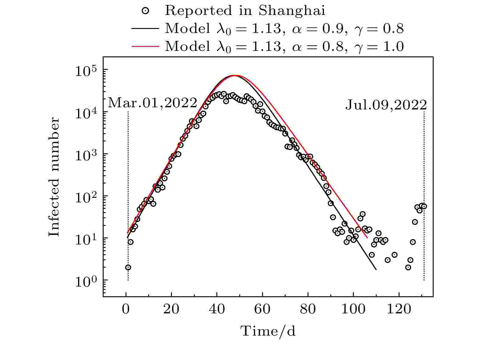
Owing to the continuous variant of the COVID-19 virus, the present epidemic may persist for a long time, and each breakout displays strongly region/time-dependent characteristics. Predicting each specific burst is the basic task for the corresponding strategies. However, the refinement of prevention and control measures usually means the limitation of the existing records of the evolution of the spread, which leads to a special difficulty in making predictions. Taking into account the interdependence of people’s travel behaviors and the epidemic spreading, we propose a modified logistic model to mimic the COVID-19 epidemic spreading, in order to predict the evolutionary behaviors for a specific bursting in a megacity with limited epidemic related records. It continuously reproduced the COVID-19 infected records in Shanghai, China in the period from March 1 to June 28, 2022. From December 7, 2022 when China adopted new detailed prevention and control measures, the COVID-19 epidemic broke out nationwide, and the infected people themselves took “ibuprofen” widely to relieve the symptoms of fever. A reasonable assumption is that the total number of searches for the word “ibuprofen” is a good representation of the number of infected people. By using the number of searching for the word “ibuprofen” provided on Baidu, a famous searching platform in China, we estimate the parameters in the modified logistic model and predict subsequently the epidemic spreading behavior in Shanghai, China starting from December 1, 2022. This situation lasted for 72 days. The number of the infected people increased exponentially in the period from the beginning to the 24th day, reached a summit on the 31st day, and decreased exponentially in the period from the 38th day to the end. Within the two weeks centered at the summit, the increasing and decreasing speeds are both significantly small, but the increased number of infected people each day was significantly large. The characteristic for this prediction matches very well with that for the number of metro passengers in Shanghai. It is suggested that the relevant departments should establish a monitoring system composed of some communities, hospitals, etc. according to the sampling principle in statistics to provide reliable prediction records for researchers.
GEOPHYSICS, ASTRONOMY, AND ASTROPHYSICS
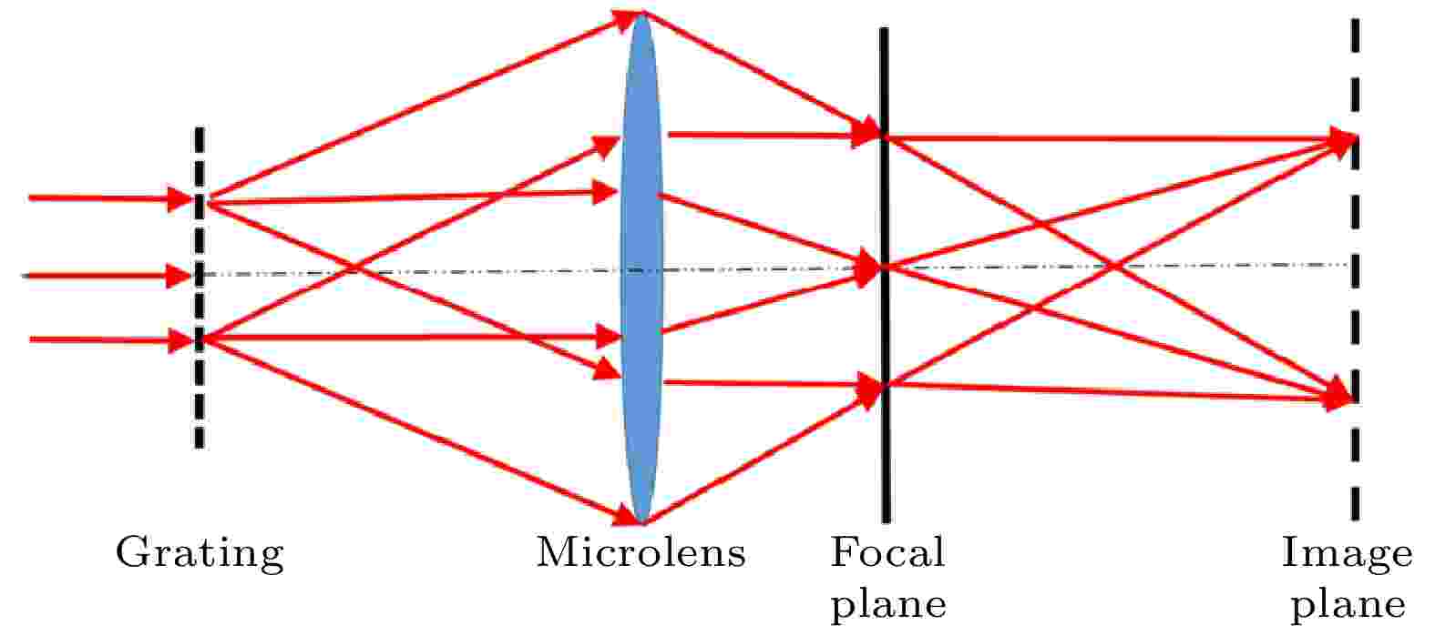
2023, 72 (9): 099501.
doi: 10.7498/aps.72.20222251
Abstract +
The microlens-assisted microscope realizes super-resolution imaging and observation, and has the advantages of no marking, no damage, real-time, localization, and good environmental compatibility. Liquid microlens arrays with uniformity and easy manipulation can realize super-resolution imaging without complicated mechanical scanning and driving. However, simply and efficiently controlling the imaging distance is a key technical challenge to the realization of super-resolution imaging of microlens. In this paper, the uniform depths of photoresist microholes on light disk are fabricated by ultraviolet exposure technology. Using liquid self-assembly technology, the microholes are filled with glycerol droplets, and thus ensuring the near-field imaging distance of the microlens. The reconfigurable super-resolution of 226-nm-wide grating line and the imaging magnification of 1.59 times are observed under the optical microscope. At present, the theory of super-resolution imaging based on microlens is not unified and perfect. In this paper, the Abbe imaging principle is used to explain the imaging magnification and super-resolution characteristics. Therefore, the liquid microlens arrays integrated on the light disk show great potential application in optical nanometer measurements and sensing devices.
