-
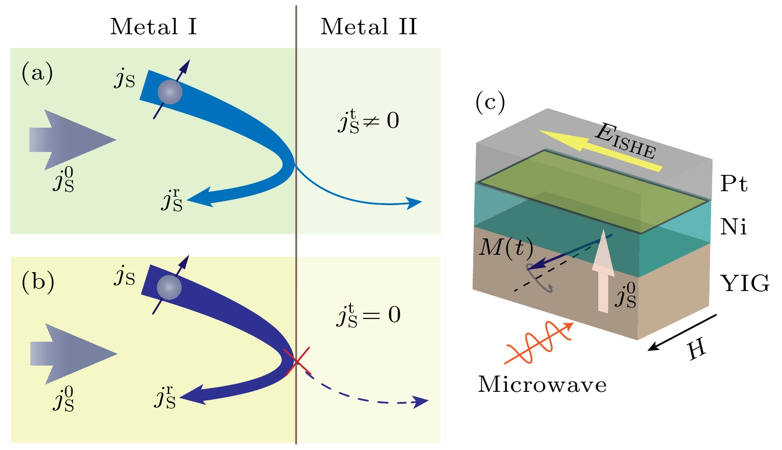
Spin current, the flow of spin angular momentum, can carry and transport energy and/or information without generating Joule heating, which makes spin-based devices become one of the potential aspects for the next-generation information processing devices. It is important to investigate the generation, transport, and detection of spins for developing spin-based devices, in which the spin transport and its related phenomena attract ongoing interest due to the complex interactions between spins and condensed matter system. Here, spin transport phenomenon is studied at a heterojunction consisting of ferromagnetic metal nickel and nonmagnetic heavy metal platinum, where transport spins are found to be totally blocked. Two series of spin-pumping devices, i.e. the yttrium iron garnet (YIG)/Ni/Pt trilayer devices and the contrastive YIG/Ni bilayer devices, are made in this work. The YIG serves as a substrate and spin-pump layer, on which nickel film and platinum film are deposited by a dc magnetron sputtering system. Spin currents are generated from YIG and injected into nickel layers by spin pumping technology. The voltage signals corresponding to the inverse spin Hall effect are detected and analyzed comparatively for both YIG/Ni/Pt trilayer device and YIG/Ni bilayer device. It is found that the platinum layers in YIG/Ni/Pt trilayer devices act only as charge current shunting but do not contribute to the spin-charge conversion. This implies that the spin current cannot transport through the Ni/Pt interface even when the nickel layer is as thin as 1 nm, in other words, the spin current is blocked at the Ni/Pt interface. Our result proposes a heterojunction that can block transport spins totally, which has never been discussed before, and the present study may expand the views and promote the development of spin-based devices.
-
Keywords:
- spin current /
- heterojunction interface /
- spin blocking /
- spin pumping
[1] Flatte M E 2007 IEEE Trans. Electron Devices 54 907
 Google Scholar
[2] Brataas A, Kent A D, Ohno H 2012 Nat. Mater. 11 372
 Google Scholar
[3] Wolf S A, Awschalom D D, Buhrman R A, Daughton J M, von Molnar S, Roukes M L, Chtchelkanova A Y, Treger D M 2001 Science 294 1488
 Google Scholar
[4] Matsuo M, Ieda J, Saitoh E, Maekawa S 2011 Phys. Rev. Lett. 106 076601
 Google Scholar
[5] Maekawa S, Adachi H, Uchida K-i, Ieda J i, Saitoh E 2013 J. Phys. Soc. Jpn. 82 102002
 Google Scholar
[6] Takahashi S, Maekawa S 2008 Sci. Technol. Adv. Mater. 9 014105
 Google Scholar
[7] Hirsch J E 1999 Phys. Rev. Lett. 83 1834
 Google Scholar
[8] Sinova J, Valenzuela S O, Wunderlich J, Back C H, Jungwirth T 2015 Rev. Mod. Phys. 87 1213
 Google Scholar
[9] Shen J, Feng Z, Xu P, Hou D, Gao Y, Jin X 2021 Phys. Rev. Lett. 126 197201
 Google Scholar
[10] Chen X, Shi S, Shi G, Fan X, Song C, Zhou X, Bai H, Liao L, Zhou Y, Zhang H, Li A, Chen Y, Han X, Jiang S, Zhu Z, Wu H, Wang X, Xue D, Yang H, Pan F 2021 Nat. Mater. 20 800
 Google Scholar
[11] Okamoto S 2016 Phys. Rev. B 93 064421
 Google Scholar
[12] Liu M, Sha R, Wang M, Peng Y, Zhang Z, Zou A, Xu Y, Guo F, Qiu Z 2021 J. Phys. D Appl. Phys. 54 155001
 Google Scholar
[13] Zhu L, Ralph D C, Buhrman R A 2019 Phys. Rev. Lett. 123 057203
 Google Scholar
[14] Ong T T, Nagaosa N 2018 Phys. Rev. Lett. 121 066603
 Google Scholar
[15] Wimmer T, Althammer M, Liensberger L, Vlietstra N, Geprags S, Weiler M, Gross R, Huebl H 2019 Phys. Rev. Lett. 123 257201
 Google Scholar
[16] Kroemer H 2001 Rev. Mod. Phys. 73 783
 Google Scholar
[17] Kurt H, Loloee R, Eid K, Pratt W P, Bass J 2002 Appl. Phys. Lett. 81 4787
 Google Scholar
[18] Nguyen H Y T, Pratt W P, Bass J 2014 J. Magn. Magn. Mater. 361 30
 Google Scholar
[19] Rojas-Sanchez J C, Reyren N, Laczkowski P, Savero W, Attane J P, Deranlot C, Jamet M, George J M, Vila L, Jaffres H 2014 Phys. Rev. Lett. 112 106602
 Google Scholar
[20] Chen K, Zhang S 2015 Phys. Rev. Lett. 114 126602
 Google Scholar
[21] Hoffmann A 2007 Phys. Status Solidi C 4 4236
 Google Scholar
[22] Yang F, Chris Hammel P 2018 J. Phys. D Appl. Phys. 51 253001
 Google Scholar
[23] Ando K, Kajiwara Y, Takahashi S, Maekawa S, Takemoto K, Takatsu M, Saitoh E 2008 Phys. Rev. B 78 014413
 Google Scholar
[24] Ando K, Takahashi S, Ieda J, Kajiwara Y, Nakayama H, Yoshino T, Harii K, Fujikawa Y, Matsuo M, Maekawa S, Saitoh E 2011 J. Appl. Phys. 109 103913
 Google Scholar
[25] Saitoh E, Ueda M, Miyajima H, Tatara G 2006 Appl. Phys. Lett. 88 182509
 Google Scholar
[26] Qiu Z, Li J, Hou D, Arenholz E, N'Diaye A T, Tan A, Uchida K, Sato K, Okamoto S, Tserkovnyak Y, Qiu Z Q, Saitoh E 2016 Nat. Commun. 7 12670
 Google Scholar
[27] Sha R, Liu Q, Wang M, Liu M, Peng Y, Zhang Z, Zou A, Xu Y, Jiang X, Qiu Z 2021 Phys. Rev. B 103 024432
 Google Scholar
[28] Qiu Z, An T, Uchida K, Hou D, Shiomi Y, Fujikawa Y, Saitoh E 2013 Appl. Phys. Lett. 103 182404
 Google Scholar
[29] Du C, Wang H, Yang F, Hammel P C 2014 Phys. Rev. B 90 140407
 Google Scholar
[30] Nakayama H, Ando K, Harii K, Yoshino T, Takahashi R, Kajiwara Y, Uchida K, Fujikawa Y, Saitoh E 2012 Phys. Rev. B 85 144408
 Google Scholar
-
图 2 (a) 自旋泵浦实验设置与YIG/Ni/Pt三层器件及YIG/Ni双层器件的结构示意图; (b) 多层器件的典型微波吸收谱; (c) YIG/Ni(3 nm)/Pt三层及YIG/Ni(3 nm)双层器件的电压信号V与外磁场H的依存关系图
Figure 2. (a) Illustration of experimental spin pumping set-up of YIG/Ni/Pt trilayer and YIG/Ni bilayer devices; (b) the typical microwave absorption spectrum; (c) the external magnetic field H dependences of the voltage signals V for the YIG/Ni(3 nm)/Pt trilayer and YIG/Ni(3 nm) bilayer devices.
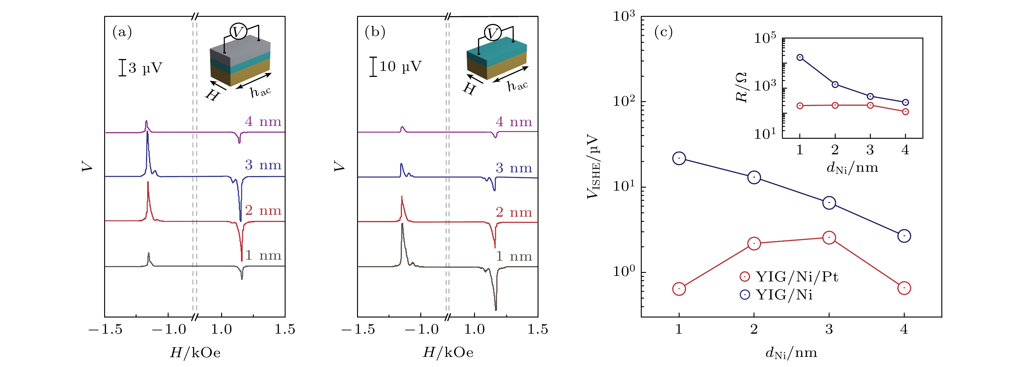
图 3 不同Ni层厚度dNi的YIG/Ni/Pt三层 (a) 及YIG/Ni双层器件 (b) 的电压信号V与外磁场H的关系; (c) 逆自旋霍尔电压VISHE 与Ni层厚度dNi的关系(插图为两种器件的横向电阻R与Ni层厚度dNi的关系)
Figure 3. The external magnetic field H dependences of the voltage signals V for the YIG/Ni/Pt trilayer devices (a) and the YIG/Ni bilayer devices (b) with different nickel layer thicknesses dNi; (c) the nickel layer thickness dNi dependences of the inverse spin Hall voltage signal VISHE for the two series of devices (the inset shows the nickel layer thickness dNi dependences of the transverse resistances R).
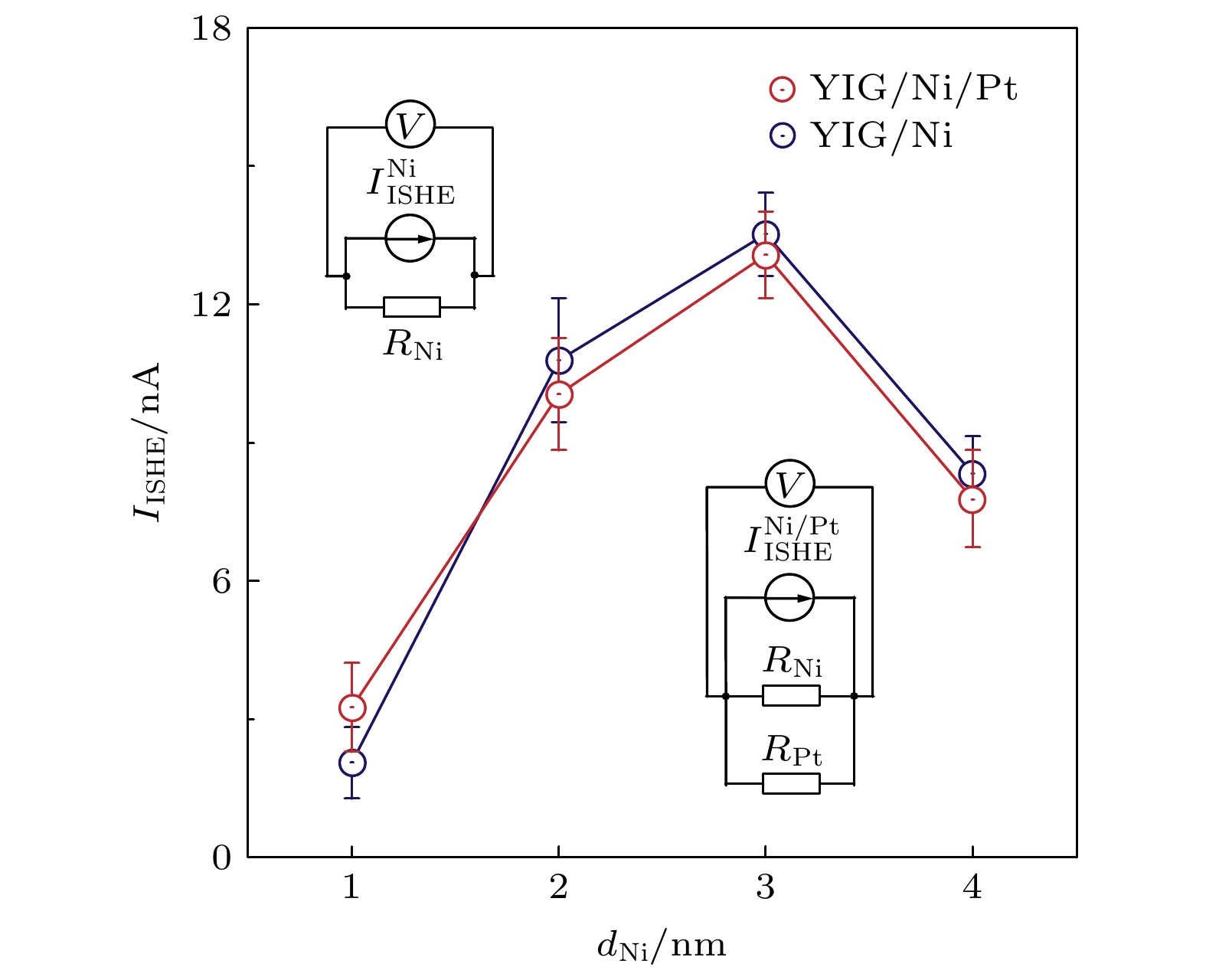
图 4 YIG/Ni/Pt三层及YIG/Ni双层器件中逆自旋霍尔电流 IISHE与Ni层厚度dNi的依存关系图(插图是两种器件中逆自旋霍尔效应测量的等效电路图)
Figure 4. The nickel layer thicknesses dNi dependences of the inverse spin Hall current IISHE for the YIG/Ni/Pt trilayer devices and the YIG/Ni bilayer devices (the insets are the equivalent circuits for inverse spin Hall measurement for the two series of devices).
-
[1] Flatte M E 2007 IEEE Trans. Electron Devices 54 907
 Google Scholar
[2] Brataas A, Kent A D, Ohno H 2012 Nat. Mater. 11 372
 Google Scholar
[3] Wolf S A, Awschalom D D, Buhrman R A, Daughton J M, von Molnar S, Roukes M L, Chtchelkanova A Y, Treger D M 2001 Science 294 1488
 Google Scholar
[4] Matsuo M, Ieda J, Saitoh E, Maekawa S 2011 Phys. Rev. Lett. 106 076601
 Google Scholar
[5] Maekawa S, Adachi H, Uchida K-i, Ieda J i, Saitoh E 2013 J. Phys. Soc. Jpn. 82 102002
 Google Scholar
[6] Takahashi S, Maekawa S 2008 Sci. Technol. Adv. Mater. 9 014105
 Google Scholar
[7] Hirsch J E 1999 Phys. Rev. Lett. 83 1834
 Google Scholar
[8] Sinova J, Valenzuela S O, Wunderlich J, Back C H, Jungwirth T 2015 Rev. Mod. Phys. 87 1213
 Google Scholar
[9] Shen J, Feng Z, Xu P, Hou D, Gao Y, Jin X 2021 Phys. Rev. Lett. 126 197201
 Google Scholar
[10] Chen X, Shi S, Shi G, Fan X, Song C, Zhou X, Bai H, Liao L, Zhou Y, Zhang H, Li A, Chen Y, Han X, Jiang S, Zhu Z, Wu H, Wang X, Xue D, Yang H, Pan F 2021 Nat. Mater. 20 800
 Google Scholar
[11] Okamoto S 2016 Phys. Rev. B 93 064421
 Google Scholar
[12] Liu M, Sha R, Wang M, Peng Y, Zhang Z, Zou A, Xu Y, Guo F, Qiu Z 2021 J. Phys. D Appl. Phys. 54 155001
 Google Scholar
[13] Zhu L, Ralph D C, Buhrman R A 2019 Phys. Rev. Lett. 123 057203
 Google Scholar
[14] Ong T T, Nagaosa N 2018 Phys. Rev. Lett. 121 066603
 Google Scholar
[15] Wimmer T, Althammer M, Liensberger L, Vlietstra N, Geprags S, Weiler M, Gross R, Huebl H 2019 Phys. Rev. Lett. 123 257201
 Google Scholar
[16] Kroemer H 2001 Rev. Mod. Phys. 73 783
 Google Scholar
[17] Kurt H, Loloee R, Eid K, Pratt W P, Bass J 2002 Appl. Phys. Lett. 81 4787
 Google Scholar
[18] Nguyen H Y T, Pratt W P, Bass J 2014 J. Magn. Magn. Mater. 361 30
 Google Scholar
[19] Rojas-Sanchez J C, Reyren N, Laczkowski P, Savero W, Attane J P, Deranlot C, Jamet M, George J M, Vila L, Jaffres H 2014 Phys. Rev. Lett. 112 106602
 Google Scholar
[20] Chen K, Zhang S 2015 Phys. Rev. Lett. 114 126602
 Google Scholar
[21] Hoffmann A 2007 Phys. Status Solidi C 4 4236
 Google Scholar
[22] Yang F, Chris Hammel P 2018 J. Phys. D Appl. Phys. 51 253001
 Google Scholar
[23] Ando K, Kajiwara Y, Takahashi S, Maekawa S, Takemoto K, Takatsu M, Saitoh E 2008 Phys. Rev. B 78 014413
 Google Scholar
[24] Ando K, Takahashi S, Ieda J, Kajiwara Y, Nakayama H, Yoshino T, Harii K, Fujikawa Y, Matsuo M, Maekawa S, Saitoh E 2011 J. Appl. Phys. 109 103913
 Google Scholar
[25] Saitoh E, Ueda M, Miyajima H, Tatara G 2006 Appl. Phys. Lett. 88 182509
 Google Scholar
[26] Qiu Z, Li J, Hou D, Arenholz E, N'Diaye A T, Tan A, Uchida K, Sato K, Okamoto S, Tserkovnyak Y, Qiu Z Q, Saitoh E 2016 Nat. Commun. 7 12670
 Google Scholar
[27] Sha R, Liu Q, Wang M, Liu M, Peng Y, Zhang Z, Zou A, Xu Y, Jiang X, Qiu Z 2021 Phys. Rev. B 103 024432
 Google Scholar
[28] Qiu Z, An T, Uchida K, Hou D, Shiomi Y, Fujikawa Y, Saitoh E 2013 Appl. Phys. Lett. 103 182404
 Google Scholar
[29] Du C, Wang H, Yang F, Hammel P C 2014 Phys. Rev. B 90 140407
 Google Scholar
[30] Nakayama H, Ando K, Harii K, Yoshino T, Takahashi R, Kajiwara Y, Uchida K, Fujikawa Y, Saitoh E 2012 Phys. Rev. B 85 144408
 Google Scholar
Catalog
Metrics
- Abstract views: 6767
- PDF Downloads: 167
- Cited By: 0


 DownLoad:


