


-
In recent years, regulating organic functional molecule has gradually received much attention in the field of materials due to its significant contribution in improving the charge carrier mobility of nanometer optoelectronic device. Molecular configuration and assembly structure of vanadyl phthalocyanine (VOPc) are systemically investigated on pristine and oxidized Cu(110) surface by using low temperature scanning tunneling microscopy. In the initial deposition stage, two molecular adsorption configurations, referring to O-up and O-down, are randomly distributed on the pristine Cu(110) surface. By oxidizing Cu(110) at different oxygen atmospheres and substrate temperatures, two different copper oxide structures are obtained, i.e. CuO-(2×1) and Cu5O6-c(6×2). The VOPc molecules are then deposited on both surfaces via thermal evaporation. For the CuO-(2×1) surface, contrastly, extended molecular chains form in the initial adsorption and subsequently the VOPc molecules assemble into an ordered molecular film involving both configurations. The VOPc molecules shows two packing orientations with a rotation angle of about 36° relative to each other. On Cu5O6-c(6×2), the O-down and O-up molecules are isolatedly adsorbed at the initial coverage. As the coverage increases, molecular assembly film gradually forms a parallelogram-shaped unit cell that involves only the O-up molecules. The molecular film exhibits two distinct molecular orientations with a rotation angle of about 42° relative to each other. The dipole-dipole interaction drives the configuration transition from the O-up configuration to O-down configuration. The O-down VOPc molecules of the second layer tend to be adsorbed on the molecular membrane supported by the Cu5O6-c(6×2) surface. The dipole-dipole interaction between neighboring molecular layers may be responsible for the preferable adsorption of the second-layered molecules. This study suggests the importance of surface oxidization in modifying configurations and orbital distributions of adsorbed molecules that can affect the charge transport in molecular films during fabricating electronic devices.
-
Keywords:
- vanadyl phthalocyanine /
- copper oxide layer /
- scanning tunneling microscopy /
- molecular assembly
[1] Salehi A, Fu X, Shin D H, So F 2019 Adv. Funct. Mater. 29 1808803
 Google Scholar
[2] Huang Y, Hsiang E L, Deng M Y, Wu S T 2020 Light Sci. Appl. 9 105
Google Scholar
[3] Park J W, Shin D C, Park S H 2011 Semicond. Sci. Technol. 26 034002
Google Scholar
[4] Lakshminarayana A N, Ong A, Chi C 2018 J. Mater. Chem. C 6 3551
Google Scholar
[5] Chase D T, Fix A G, Kang S J, Rose B D, Weber C D, Zhong Y, Zakharov L N, Lonergan M C, Nuckolls C, Haley M M 2012 J. Am. Chem. Soc. 134 10349
Google Scholar
[6] Yan Y, Zhao Y, Liu Y 2022 J. Polym. Sci. 60 311
Google Scholar
[7] Brabec C J, Distler A, Du X, Egelhaaf H J, Hauch J, Heumueller T, Li N 2020 Adv. Eng. Mater. 10 2001864
Google Scholar
[8] Wang Z, Gao K, Kan Y, Zhang M, Qiu C, Zhu L, Zhao Z, Peng X, Feng W, Qian Z, Gu X, Jen A K Y, Tang B Z, Cao Y, Zhang Y, Liu F 2021 Nat. Commun. 12 332
Google Scholar
[9] Gao K, Zhu Z, Xu B, Jo S B, Kan Y, Peng X, Jen A K Y 2017 Adv. Mater. 29 1703980
Google Scholar
[10] Hofmann O T, Zojer E, Hörmann L, Jeindl A, Maurer R J 2021 Phys. Chem. Chem. Phys. 23 8132
Google Scholar
[11] Street R A 2016 Adv. Mater. 28 3814
Google Scholar
[12] Li P, Lu Z H 2021 Small Sci. 1 2000015
Google Scholar
[13] Shen Q, Sun X, Chen X, Li R, Li X, Chen S 2023 Device 1 100061
Google Scholar
[14] He D, Qiao J, Zhang L, Wang J, Lan T, Qian J, Li Y, Shi Y, Chai Y, Lan W, Ono L K, Qi Y, Xu J, Ji W, Wang X 2017 Sci. Adv. 3 e1701186
Google Scholar
[15] Yang F, Cheng S, Zhang X, Ren X, Li R, Dong H, Hu W 2018 Adv. Mater. 30 1702415
Google Scholar
[16] Jin E, Geng K, Fu S, Yang S, Kanlayakan N, Addicoat M A, Kungwan N, Geurs J, Xu H, Bonn M, Wang H I, Smet J, Kowalczyk T, Jiang D 2021 Chem 7 3309
Google Scholar
[17] Dou L, Wong A B, Yu Y, Lai M, Kornienko N, Eaton S W, Fu A, Bischak C G, Ma J, Ding T, Ginsberg N S, Wang L, Alivisatos A P , Yang P 2015 Sciences 349 1518
Google Scholar
[18] Xiong P, Wu Y, Liu Y, Ma R, Sasaki T, Wang X, Zhu J 2020 Energy Environ. 13 4834
Google Scholar
[19] Coppedè N, Bonnini E, Mezzadri F, Tarabella G, Ranzieri P, Barba L, Arrighetti G, Lutterotti L, Iannotta, S 2016 Org. Electron. 32 15
Google Scholar
[20] Sun C, Ran X, Wang X, Cheng Z, Wu Q, Cai S, Gu L, Gan N, Shi H, An Z, Shi H, Huang W 2018 J. Phys. Chem. Lett. 9 335
Google Scholar
[21] Xie W, Wang X, Xu J 2012 J. Phys. Chem. C 116 17580
Google Scholar
[22] Paes L W C, Suarez J A, Márquez A M, Cruz A G B d, Sanz J F 2019 Theor. Chem. Acc. 138 88
Google Scholar
[23] Kolotovska V, Friedrich M, Zahn D R T, Salvan G 2006 J. Cryst. 291 166
Google Scholar
[24] Zhong Y, Huang M, Huang G, Lu S, Guo Q, Yu Y 2021 Vacuum 186 110036
Google Scholar
[25] Lu S, Huang M, Qin Z, Yu Y, Guo Q, Cao G 2018 Nanotechnology 29 315301
Google Scholar
[26] Mattioli G, Filippone F, Bonapasta A A 2010 J. Phys. Chem. Lett. 1 2757
Google Scholar
[27] Zhang Q, Wang D, Xu J, Cao J, Sun J, Wang M 2003 Mater. Chem. Phys. 82 525
Google Scholar
[28] Zhu H, Song H, Zhao W, Peng Z, Liu D, Di B, Xing L, Chen H, Huang Z C, Wang Y, Wu K 2019 J. Phys. Chem. C 23 17390
Google Scholar
[29] Malavolti L, Briganti M, Hänze M, Serrano G, Cimatti I, McMurtrie G, Otero E, Ohresser P, Totti F, Mannini M, Sessoli R, Loth S 2018 Nano Lett. 18 7955
Google Scholar
[30] Liu Y, Ma L, Shen C, Wang X, Zhou X, Zhao Z, Xu A 2019 Chin. J. Catal. 40 168
Google Scholar
[31] Wang H, Song D, Yang J, Yu B, Geng Y, Yan D 2007 Appl. Phys. Lett. 90 253510
Google Scholar
[32] Barlow D E, Hipps K W 2000 J. Phys. Chem. B 104 5993
Google Scholar
[33] Niu T, Zhang J, Chen W 2014 J. Phys. Chem. C 118 4151
Google Scholar
[34] Eguchi K, Takagi Y, Nakagawa T, Yokoyama T 2013 J. Phys. Chem. C 117 22843
Google Scholar
[35] Adler H, Paszkiewicz M, Uihlein J, Polek M, Ovsyannikov R, Basova T V, Chassé T, Peisert H 2015 J. Phys. Chem. C 119 8755
Google Scholar
[36] Rochford L A, Ramadan A J, Woodruff D P, Heutz S, Jones T S 2015 Phys. Chem. Chem. Phys. 17 29747
Google Scholar
[37] Wang Y F, Kröger J, Berndt R, Vázquez H, Brandbyge M, Paulsson M 2010 Phys. Rev. Lett. 104 176802
Google Scholar
[38] Zhang J, Wang Z, Niu T, Li Z, Chen W 2014 Appl. Phys. Lett. 104 113506
Google Scholar
[39] Niu T, Zhou M, Zhang J, Feng Y, Chen W 2013 J. Phys. Chem. C 117 1013
Google Scholar
[40] Guillemot L, Bobrov K 2011 Phys. Rev. B 83 075409
Google Scholar
[41] Fukagawa H, Hosoumi S, Yamane H, Kera S, Ueno N 2011 Phys. Rev. B 83 085304
Google Scholar
[42] Duan X, Warschkow O, Soon A, Delley B, Stampfl C 2010 Phys. Rev. B 81 075430
Google Scholar
-

图 1 (a) VOPc分子结构模型的侧视图和俯视图; (b) 在0.2 MLE 覆盖度下获得的STM形貌图 (24 nm × 24 nm, U = 0.5 V, I = 0.1 nA), 蓝色圆圈和红色圆圈分别标识出氧原子向上和氧原子向下两种分子构型
Figure 1. (a) Side view and top view of the VOPc structural model; (b) STM topography obtained at 0.2 MLE coverage (24 nm × 24 nm, U = 0.5 V, I = 0.1 nA). Blue and red circles highlight the O-up and O-down configurations of absorbed VOPc molecules, respectively.
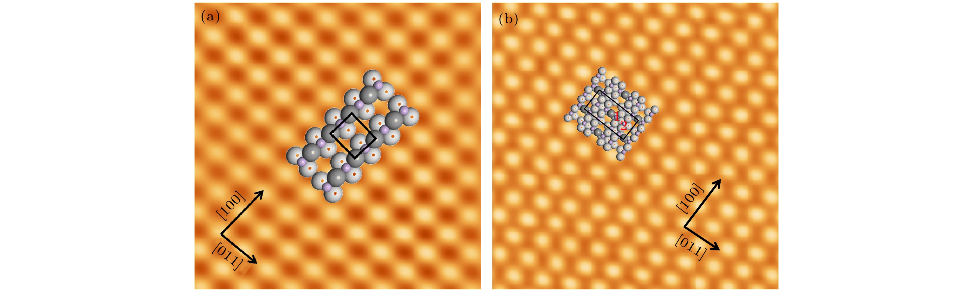
图 2 (a) 衬底温度保持在520 K下制备的CuO-(2×1)氧化层的原子分辨STM图和其结构模型图 (4 nm × 4 nm, U = –0.5 V, I = –0.1 nA); (b) 衬底温度保持在700 K下制备的Cu5O6-c(6×2)氧化层的原子分辨STM和其结构模型图 (9 nm × 9 nm, U = 0.2 V, I = 0.2 nA). 灰色球和白色球代表铜原子, 紫色球代表氧原子. 两种不等价的氧原子分别用数字“1”和“2”标识
Figure 2. (a) Atomic resolution STM image obtained on the CuO-(2×1) surface (4 nm × 4 nm, U = –0.5 V, I = –0.1 nA), the structural model of CuO-(2×1) is superimposed onto it; (b) atomic resolution STM image obtained on the Cu5O6-c(6×2) surface (9 nm × 9 nm, U = 0.2 V, I = 0.2 nA). The structural model of Cu5O6-c(6×2) is superimposed onto it. In the structural models, the gray and white balls represent the topmost and underlying copper atoms, respectively. The purple balls represent the oxygen atoms. Two unequal oxygen atoms are denoted by the numbers “1” and “2”.
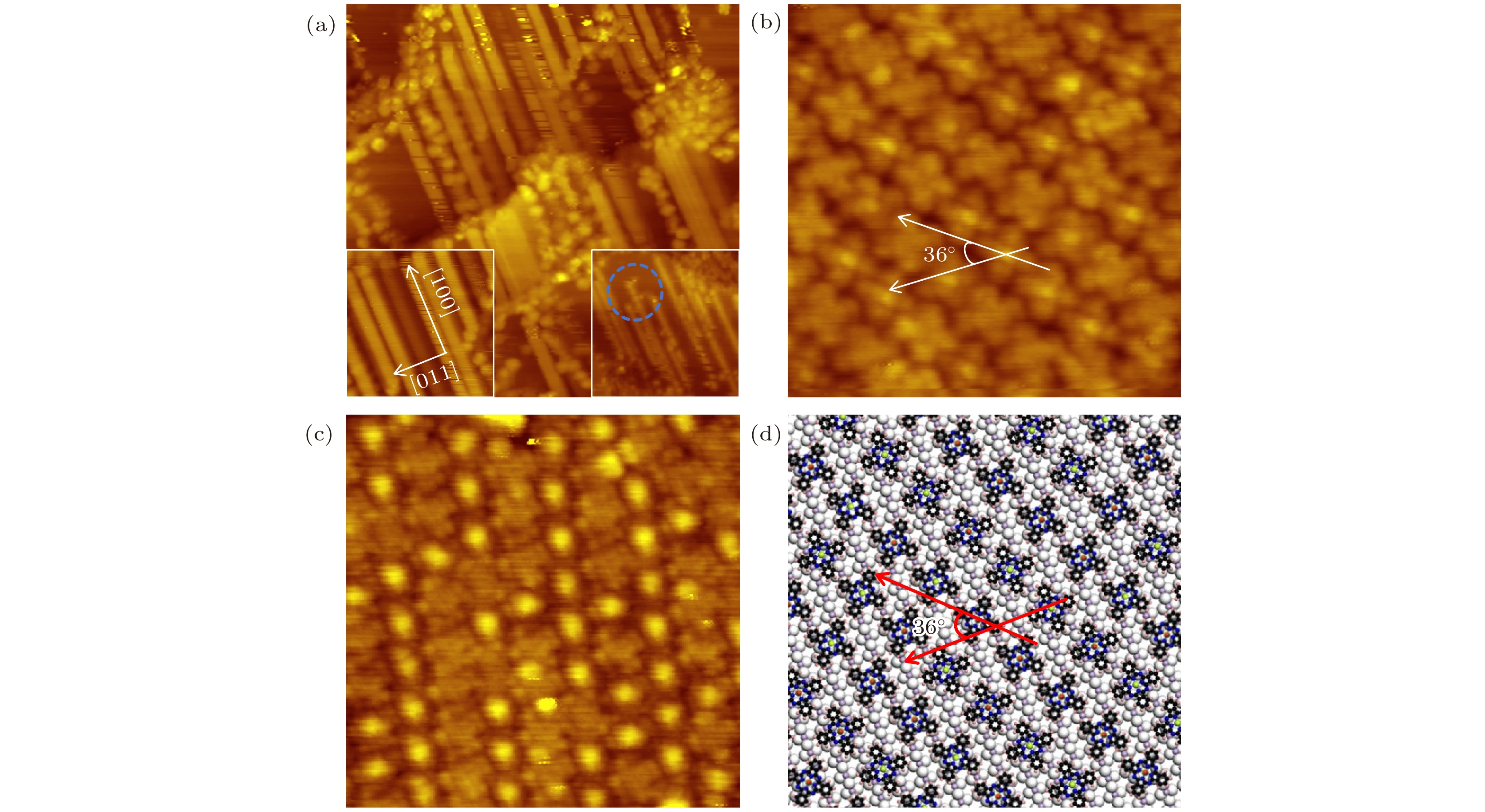
图 3 (a) 0.25 MLE VOPc分子沉积在CuO-(2×1)表面上后获得的STM形貌图 (64 nm × 64 nm, U = 1.0 V, I = 0.1 nA), 右插图显示VOPc分子在氧化层表面上形成了分子链结构, 并不是VOPc分子沿着台面迁移 (29 nm × 29 nm, U = 2.0 V, I = 0.2 nA), 左插图显示所有分子链沿Cu(110)表面的[100]方向排列 (24 nm × 24 nm, U = 1.0 V, I = 0.1 nA); (b) 覆盖度增加到大约一个单层时获得的亚分子分辨的STM形貌图, 吸附的VOPc分子组装为具有$ {C}_{6} $对称性的有序膜, 相邻分子取向的夹角约为36° (10 nm × 10 nm, U = 1.0 V, I = 0.1 nA); (c) 针尖顶端被分子碎片功能化后获得的STM形貌图 (13.7 nm × 13.7 nm, U = 1.0 V, I = 0.1 nA); (d) 对应图(b)的可能组装模型图
Figure 3. (a) STM image recorded on the CuO-(2×1) surface with the VOPc coverage of about 0.25 MLE (64 nm × 64 nm, U = 1.0 V, I = 0.1 nA). The right inset shows that VOPc molecules form extended molecular chains instead of molecular diffusion on the terrace (29 nm × 29 nm, U = 2.0 V, I = 0.2 nA). The left inset shows the zoomed STM image which reveals the molecular chains align along the [100] direction (24 nm × 24 nm, U = 1.0 V, I = 0.1 nA). (b) STM topography obtained at the VOPc coverage of about 1.0 MLE. The angle between adjacent molecular orientations is about 36° (10 nm × 10 nm, U = 1.0 V, I = 0.1 nA). (c) STM topography obtained by using a functionalized tip (13.7 nm × 13.7 nm, U = 1.0 V, I = 0.1 nA). (d) The proposed assembly model of panel (b).
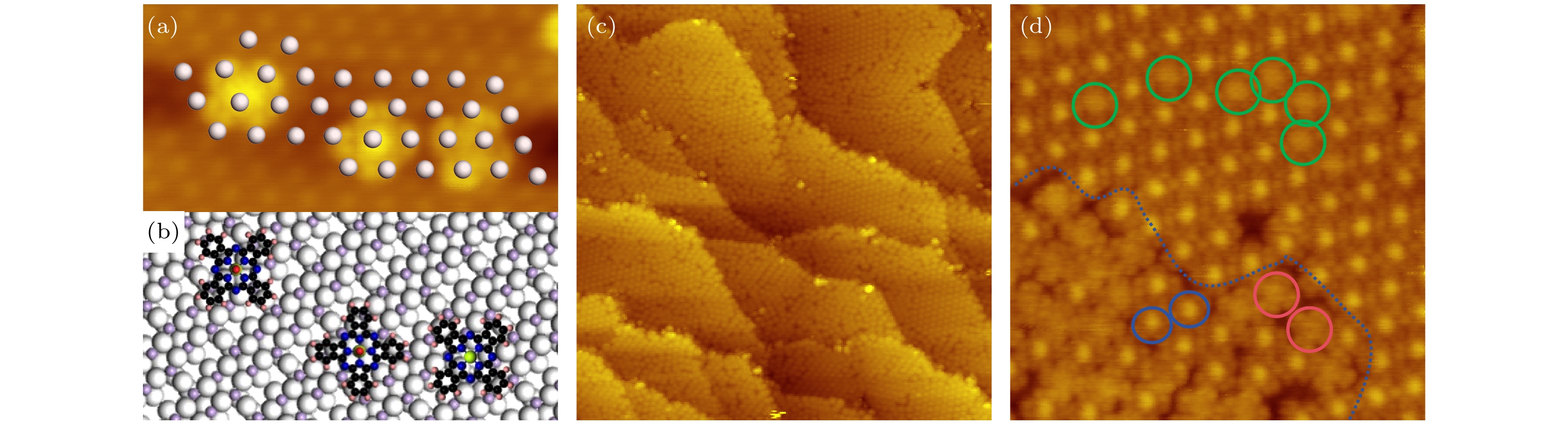
图 4 (a) 0.2 MLE VOPc分子沉积在Cu5O6-c(6×2)表面后获得的原子分辨STM形貌图 (10 nm × 6 nm, U = 1.5 V, I = 0.2 nA); (b)图(a)对应的分子吸附结构模型图; (c) 当覆盖度约为0.6 MLE时获得的STM形貌图, 可见部分VOPc分子组装成了有序结构 (94 nm × 94 nm, U= 1.5 V, I = 0.2 nA); (d) 扫描区域缩小后的STM图像, 其中有序结构和无序结构用蓝色虚线分隔开, 氧原子向上构型用蓝色圆圈标识, 氧原子向下构型用红色和绿色圆圈标识 (17 nm × 17 nm, U = 1.0 V, I = 0.2 nA)
Figure 4. (a) Atomic resolution STM image recorded on the Cu5O6-c(6×2) surface with the VOPc coverage of about 0.2 MLE (10 nm × 6 nm, U = 1.5 V, I = 0.2 nA). (b) The possible adsorption model of VOPc corresponding to panel (a). (c) STM topography obtained at the 0.6 MLE coverage (94 nm × 94 nm, U = 1.5 V, I = 0.2 nA). (d) Zoomed STM image. Ordered and disordered structures are separated by the blue curve. The blue circles denote the O-up molecules. The red and green circles highlight the O-down molecules (17 nm × 17 nm, U = 1.0 V, I = 0.2 nA).
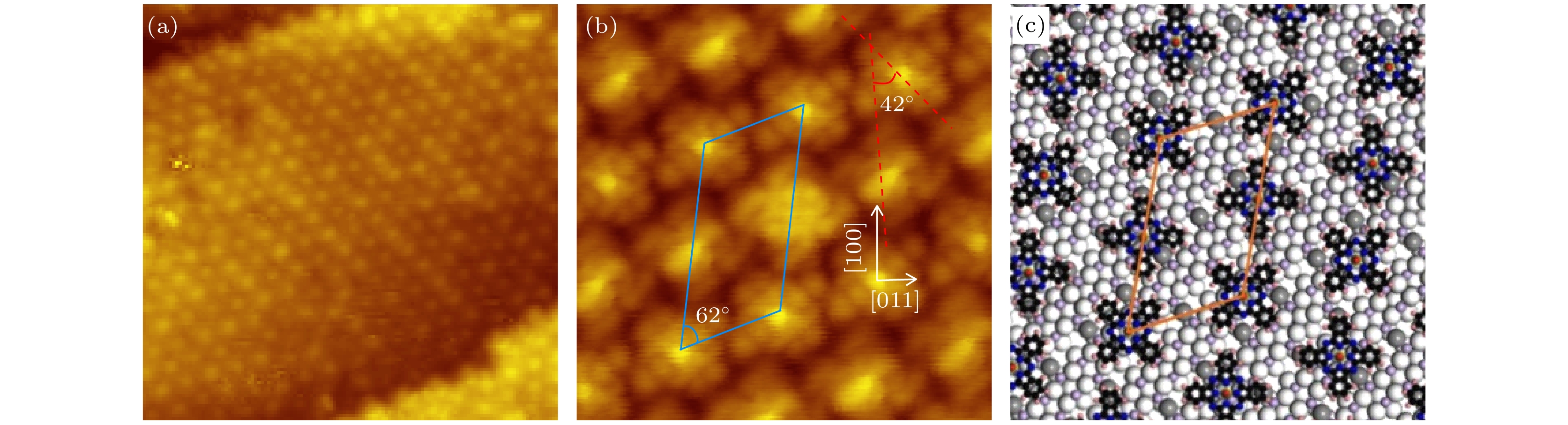
图 5 (a) 0.9 MLE VOPc分子沉积在Cu5O6-c(6×2)表面后获得的STM形貌图 (24 nm × 24 nm, U = 2.5 V, I = 0.2 nA); (b) 当覆盖度约为一个单层时获得的具有亚分子分辨的STM图像 (6.4 nm × 6.4 nm, U = 0.5 V, I = 0.2 nA), 平行四边形单胞用蓝线表示, 相邻两分子取向的夹角约为42°; (c)图(b)对应的分子组装结构模型图, 结构单胞用橙色四边形表示
Figure 5. (a) STM image recorded on the Cu5O6-c(6×2) surface with the VOPc coverage of about 0.9 MLE (24 nm × 24 nm, U = 2.5 V, I = 0.2 nA). (b) The submolecular resolution STM topography obtained at the coverage of about 1.0 MLE (6.4 nm × 6.4 nm, U = 0.5 V, I = 0.2 nA). The blue parallelogram indicates the unit cell of the molecular membrane. The angle between the orientations of two adjacent molecules is about 42° as denoted. (c) Proposed structure model of the VOPc assembly. The unit cell is indicated by an orange parallelogram.

图 6 (a) 在Cu5O6-c(6×2)表面上沉积约0.2 MLE锑原子并吸附约1.1 MLE VOPc分子后获得的STM形貌图 (47 nm × 22 nm, U = 2.0 V, I = 0.2 nA), 图中存在两种不同的组装结构; (b)扫描区域缩小后获得的STM图像 (26 nm × 24 nm, U = 2.0 V, I = 0.2 nA), 两种不同的组装结构用绿色虚线分隔; (c) 在Cu5O6区域缩小扫描范围后获得的STM 形貌图 (15.6 nm × 15.6 nm, U = 2.0 V, I = 0.2 nA)
Figure 6. (a) STM image obtained on the Cu5O4-c(6×2) surface with about 0.2 MLE Sb deposition and followed 1.1 MLE VOPc adsorption (47 nm × 22 nm, U = 2.0 V, I = 0.2 nA). (b) Zoomed STM image (26 nm × 24 nm, U = 2.0 V, I = 0.2 nA). Two kinds of assembly structures are separated by a green curve. (c) Zoomed STM image obtained on the Cu5O6-c(6×2) region (15.6 nm × 15.6 nm, U = 2.0 V, I = 0.2 nA).
-
[1] Salehi A, Fu X, Shin D H, So F 2019 Adv. Funct. Mater. 29 1808803
Google Scholar
[2] Huang Y, Hsiang E L, Deng M Y, Wu S T 2020 Light Sci. Appl. 9 105
Google Scholar
[3] Park J W, Shin D C, Park S H 2011 Semicond. Sci. Technol. 26 034002
Google Scholar
[4] Lakshminarayana A N, Ong A, Chi C 2018 J. Mater. Chem. C 6 3551
Google Scholar
[5] Chase D T, Fix A G, Kang S J, Rose B D, Weber C D, Zhong Y, Zakharov L N, Lonergan M C, Nuckolls C, Haley M M 2012 J. Am. Chem. Soc. 134 10349
Google Scholar
[6] Yan Y, Zhao Y, Liu Y 2022 J. Polym. Sci. 60 311
Google Scholar
[7] Brabec C J, Distler A, Du X, Egelhaaf H J, Hauch J, Heumueller T, Li N 2020 Adv. Eng. Mater. 10 2001864
Google Scholar
[8] Wang Z, Gao K, Kan Y, Zhang M, Qiu C, Zhu L, Zhao Z, Peng X, Feng W, Qian Z, Gu X, Jen A K Y, Tang B Z, Cao Y, Zhang Y, Liu F 2021 Nat. Commun. 12 332
Google Scholar
[9] Gao K, Zhu Z, Xu B, Jo S B, Kan Y, Peng X, Jen A K Y 2017 Adv. Mater. 29 1703980
Google Scholar
[10] Hofmann O T, Zojer E, Hörmann L, Jeindl A, Maurer R J 2021 Phys. Chem. Chem. Phys. 23 8132
Google Scholar
[11] Street R A 2016 Adv. Mater. 28 3814
Google Scholar
[12] Li P, Lu Z H 2021 Small Sci. 1 2000015
Google Scholar
[13] Shen Q, Sun X, Chen X, Li R, Li X, Chen S 2023 Device 1 100061
Google Scholar
[14] He D, Qiao J, Zhang L, Wang J, Lan T, Qian J, Li Y, Shi Y, Chai Y, Lan W, Ono L K, Qi Y, Xu J, Ji W, Wang X 2017 Sci. Adv. 3 e1701186
Google Scholar
[15] Yang F, Cheng S, Zhang X, Ren X, Li R, Dong H, Hu W 2018 Adv. Mater. 30 1702415
Google Scholar
[16] Jin E, Geng K, Fu S, Yang S, Kanlayakan N, Addicoat M A, Kungwan N, Geurs J, Xu H, Bonn M, Wang H I, Smet J, Kowalczyk T, Jiang D 2021 Chem 7 3309
Google Scholar
[17] Dou L, Wong A B, Yu Y, Lai M, Kornienko N, Eaton S W, Fu A, Bischak C G, Ma J, Ding T, Ginsberg N S, Wang L, Alivisatos A P , Yang P 2015 Sciences 349 1518
Google Scholar
[18] Xiong P, Wu Y, Liu Y, Ma R, Sasaki T, Wang X, Zhu J 2020 Energy Environ. 13 4834
Google Scholar
[19] Coppedè N, Bonnini E, Mezzadri F, Tarabella G, Ranzieri P, Barba L, Arrighetti G, Lutterotti L, Iannotta, S 2016 Org. Electron. 32 15
Google Scholar
[20] Sun C, Ran X, Wang X, Cheng Z, Wu Q, Cai S, Gu L, Gan N, Shi H, An Z, Shi H, Huang W 2018 J. Phys. Chem. Lett. 9 335
Google Scholar
[21] Xie W, Wang X, Xu J 2012 J. Phys. Chem. C 116 17580
Google Scholar
[22] Paes L W C, Suarez J A, Márquez A M, Cruz A G B d, Sanz J F 2019 Theor. Chem. Acc. 138 88
Google Scholar
[23] Kolotovska V, Friedrich M, Zahn D R T, Salvan G 2006 J. Cryst. 291 166
Google Scholar
[24] Zhong Y, Huang M, Huang G, Lu S, Guo Q, Yu Y 2021 Vacuum 186 110036
Google Scholar
[25] Lu S, Huang M, Qin Z, Yu Y, Guo Q, Cao G 2018 Nanotechnology 29 315301
Google Scholar
[26] Mattioli G, Filippone F, Bonapasta A A 2010 J. Phys. Chem. Lett. 1 2757
Google Scholar
[27] Zhang Q, Wang D, Xu J, Cao J, Sun J, Wang M 2003 Mater. Chem. Phys. 82 525
Google Scholar
[28] Zhu H, Song H, Zhao W, Peng Z, Liu D, Di B, Xing L, Chen H, Huang Z C, Wang Y, Wu K 2019 J. Phys. Chem. C 23 17390
Google Scholar
[29] Malavolti L, Briganti M, Hänze M, Serrano G, Cimatti I, McMurtrie G, Otero E, Ohresser P, Totti F, Mannini M, Sessoli R, Loth S 2018 Nano Lett. 18 7955
Google Scholar
[30] Liu Y, Ma L, Shen C, Wang X, Zhou X, Zhao Z, Xu A 2019 Chin. J. Catal. 40 168
Google Scholar
[31] Wang H, Song D, Yang J, Yu B, Geng Y, Yan D 2007 Appl. Phys. Lett. 90 253510
Google Scholar
[32] Barlow D E, Hipps K W 2000 J. Phys. Chem. B 104 5993
Google Scholar
[33] Niu T, Zhang J, Chen W 2014 J. Phys. Chem. C 118 4151
Google Scholar
[34] Eguchi K, Takagi Y, Nakagawa T, Yokoyama T 2013 J. Phys. Chem. C 117 22843
Google Scholar
[35] Adler H, Paszkiewicz M, Uihlein J, Polek M, Ovsyannikov R, Basova T V, Chassé T, Peisert H 2015 J. Phys. Chem. C 119 8755
Google Scholar
[36] Rochford L A, Ramadan A J, Woodruff D P, Heutz S, Jones T S 2015 Phys. Chem. Chem. Phys. 17 29747
Google Scholar
[37] Wang Y F, Kröger J, Berndt R, Vázquez H, Brandbyge M, Paulsson M 2010 Phys. Rev. Lett. 104 176802
Google Scholar
[38] Zhang J, Wang Z, Niu T, Li Z, Chen W 2014 Appl. Phys. Lett. 104 113506
Google Scholar
[39] Niu T, Zhou M, Zhang J, Feng Y, Chen W 2013 J. Phys. Chem. C 117 1013
Google Scholar
[40] Guillemot L, Bobrov K 2011 Phys. Rev. B 83 075409
Google Scholar
[41] Fukagawa H, Hosoumi S, Yamane H, Kera S, Ueno N 2011 Phys. Rev. B 83 085304
Google Scholar
[42] Duan X, Warschkow O, Soon A, Delley B, Stampfl C 2010 Phys. Rev. B 81 075430
Google Scholar

 DownLoad:
Catalog
Metrics
- Abstract views: 4112
- PDF Downloads: 88
- Cited By: 0
