-
Diamond coating has many excellent properties such as extreme hardness, high elastic modulus, high thermal conductivity, low friction coefficient, low thermal expansion coefficient, and good corrosion resistance. Those properties are close to natural diamond’s, thereby making the diamond coating an ideal new type of wear-resistant tool coating material. However, a large number of experiments have proved that during the deposition of diamond coating, the bonding phase cobalt on the surface of impregnated diamond substrate will generate a layer of graphite at the interface, which seriously weakens the adhesive strength between the substrate and the coating. To thoroughly solve this problem, it is necessary to investigate the microscopic process of graphitization caused by the Co element embedded on the substrate surface. Therefore, the first principle theory is adopted to simulate and analyze the interfacial adhesive strength of diamond coating when Co atom is embedded at different depths on the surface of impregnated diamond substrate, thereby exploring the mechanism of the influence of bonding phase Co element in the substrate on the diamond coating and the mechanism of Co promoting diamond graphitization. The calculation results show that the interfacial binding energy first decreases and then increases with the increase of Co embedding depth in the substrate. When Co atom is embedded in the third layer, obvious graphite structures are prone to appear at the interface, and Co promotes diamond graphitization most significantly, resulting in the minimum bonding strength between the film and substrate interface. The results of structure and charge indicate that under the influence of surface effect and Co—C bond length, the C atoms in the second layer of the substrate move to the first layer and the hybridization mode changes from sp3 to sp2. Meanwhile, this movement leads to an increase in the interaction space and quantity between Co atoms and the surrounding C atoms. In addition, there are many unpaired electrons in the Co valence layer, which can easily mix and rearrange electron orbitals with the surrounding C atoms, ultimately resulting in a graphite structure on the substrate surface. When Co atoms are embedded in the fifth layer, the stable configuration of the substrate surface and the interfacial adhesive strength are no longer affected.
-
Keywords:
- diamond coating /
- Co element /
- adhesive strength /
- graphitization
[1] Yan B, He N, Chen N, Weigold M, Chen H W, Sun S C, Wu Y, Fu S Y, Li L, Abele E 2025 Int. J. Extrem. Manuf. 7 015106
 Google Scholar
[2] Du Y F, Xie F M, Wang J, Xu B, Chen H Y, Yan B N, Wu Y J, Huang W F, Li H 2023 Materials 16 3640
 Google Scholar
[3] Wheeler D W, Wood R J K 2024 Wear 556–557 205488
 Google Scholar
[4] 简小刚, 张允华 2015 物理学报 64 046701
 Google Scholar
Jian X G, Zhang Y H 2015 Acta Phys. Sin. 64 046701
 Google Scholar
[5] Wang X L, Wu X, Lu K, Ye J W 2025 Diam. Relat. Mater. 152 111886.
 Google Scholar
[6] Liu X W, Zhang H, Lin G L, Wang Z G, Zhang J L, Shi H Y 2023 Vacuum 217 112562
 Google Scholar
[7] Tian Q Q, Huang N, Yang B, Zhuang H, Wang C, Zhai Z F, Li G H, Jia X Y, Liu L S, Jiang X 2017 J. Mater. Sci. Technol. 33 1097
 Google Scholar
[8] Li X J, He L L, Li Y S, Yang Q 2019 Surf. Coat. Technol. 360 20
 Google Scholar
[9] Saiki Y, Bando T, Harigai T, Takikawa Hirofumi, Hattori T, Sugita H, Kawahara, N, Tanaka K 2023 Diam. Relat. Mater. 132 109643
 Google Scholar
[10] Qiao Y, Nie S Y, Li W H, Liu E Z, Wang X C 2023 Appl. Surf. Sci. 633 157589
 Google Scholar
[11] Sedov V, Martyanov A, Ashkinazi E, Tiazhelov I, Savin S, Sovyk D, Mandal S, Fedorov S, Grigoriev S, Ralchenko V 2023 Surf. Interfaces 38 102861
 Google Scholar
[12] 简小刚, 陈军 2015 物理学报 64 216701
 Google Scholar
Jian X G, Chen J 2015 Acta Phys. Sin. 64 216701
 Google Scholar
[13] Sarangi S K, Chattopadhyay A, Chattopadhyay A K 2008 Appl. Surf. Sci. 254 3721
 Google Scholar
[14] Hu J B, Jian X G 2022 Mod. Phys. Lett. B 36 2250086
 Google Scholar
[15] 范舒瑜, 匡同春, 林松盛, 代明江 2023 材料导报 37 28
 Google Scholar
Fan S Y, Kuang T C, Lin S S, Dai M J 2023 Mater. Rep. 37 28
 Google Scholar
[16] Donnet J B, Paulmier D, Oulanti H 2004 Carbon 42 2215
 Google Scholar
[17] Lloret F, Soto B, Rouzbahani R, Gutiérrez M, Haenen K, Araujo D 2023 Diam. Relat. Mater. 133 109746
 Google Scholar
[18] Zhu P, Zhang Q, Xia Y X, Ma Y F, Gou H S, Liang X, Wu G H 2024 Mater. Today Phys. 48 101563
 Google Scholar
[19] Hu J B, Jian X G, Yang T, Peng X Y 2022 Diam. Relat. Mater. 123 108864
 Google Scholar
[20] Bi K, Liu J, Dai Q X 2012 Appl. Surf. Sci. 258 4581
 Google Scholar
[21] Pang X Z, Yang X Y, Yang J B, Zhao Y J, Pang M J 2021 Diam. Relat. Mater. 113 108297
 Google Scholar
[22] Ernzerhof M, Scuseria G E 1999 J. Chem. Phys. 110 5029
 Google Scholar
[23] Perdew J P, Burke K, Ernzerhof M 1996 Phys. Rev. Lett. 77 3865
 Google Scholar
[24] Chadi D J 1977 Phys. Rev. B 16 1746
 Google Scholar
[25] Jin S S, You Z Y, Han P D, Jiang A X, Sun C L, Wang L B, Zhang T, Liu S L 2024 Comput. Mater. Sci. 244 113235
 Google Scholar
-
图 3 孕镶金刚石基底金刚石涂层膜基界面模型 (a) Co在第1层; (b) Co在第2层; (c) Co在第3层; (d) Co在第4层; (e) Co在第5层; (f)不含Co
Figure 3. Interface model between impregnated diamond substrate and diamond coating: (a) Co atom doped in the first layer; (b) Co atom doped in the second layer; (c) Co atom doped in the third layer; (d) Co atom doped in the fourth layer; (e) Co atom doped in the fifth layer; (f) without Co atom.
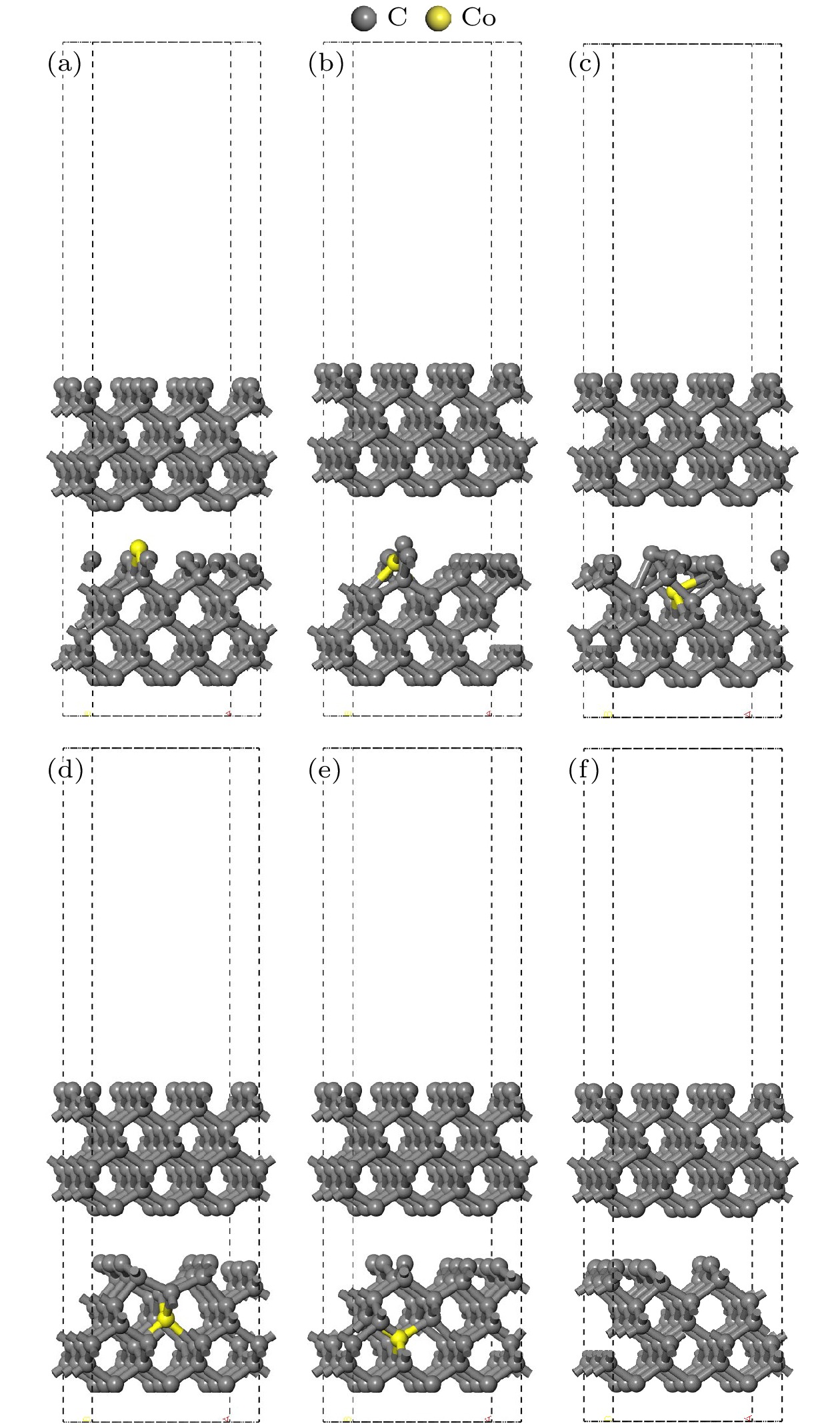
图 4 结构优化后的孕镶金刚石基底模型 (a) Co在第1层; (b) Co在第2层; (c) Co在第3层; (d) Co在第4层; (e) Co在第5层; (f)不含Co
Figure 4. Impregnated diamond substrate model after structural optimization: (a) Co atom doped in the first layer; (b) Co atom doped in the second layer; (c) Co atom doped in the third layer; (d) Co atom doped in the fourth layer; (e) Co atom doped in the fifth layer; (f) no Co atom.
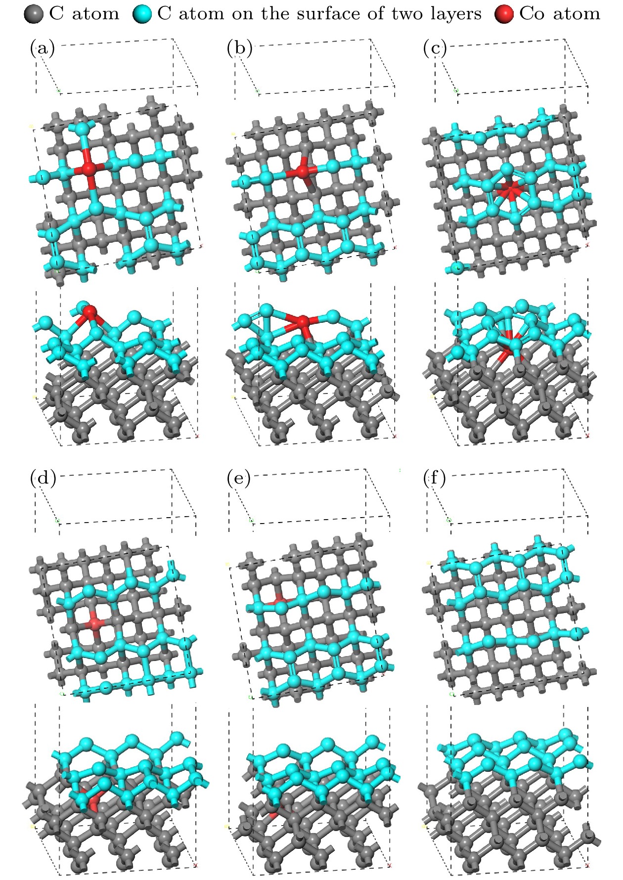
图 6 结构优化后的孕镶金刚石基底和金刚石涂层的界面模型 (a) Co在第1层; (b) Co在第2层; (c) Co在第3层; (d) Co在第4层; (e) Co在第5层; (f)不含Co
Figure 6. Interface model between impregnated diamond substrate and diamond coating after structural optimization: (a) Co atom doped in the first layer; (b) Co atom doped in the second layer; (c) Co atom doped in the third layer; (d) Co atom doped in the fourth layer; (e) Co atom doped in the fifth layer; (f) no Co atom.
图 7 基底差分电荷密度图 (a) Co在第1层; (b) Co在第2层; (c) Co在第3层; (d) Co在第4层; (e) Co在第5层
Figure 7. Differential charge density of substrate: (a) Co atom doped in the first layer; (b) Co atom doped in the second layer; (c) Co atom doped in the third layer; (d) Co atom doped in the fourth layer; (e) Co atom doped in the fifth layer.
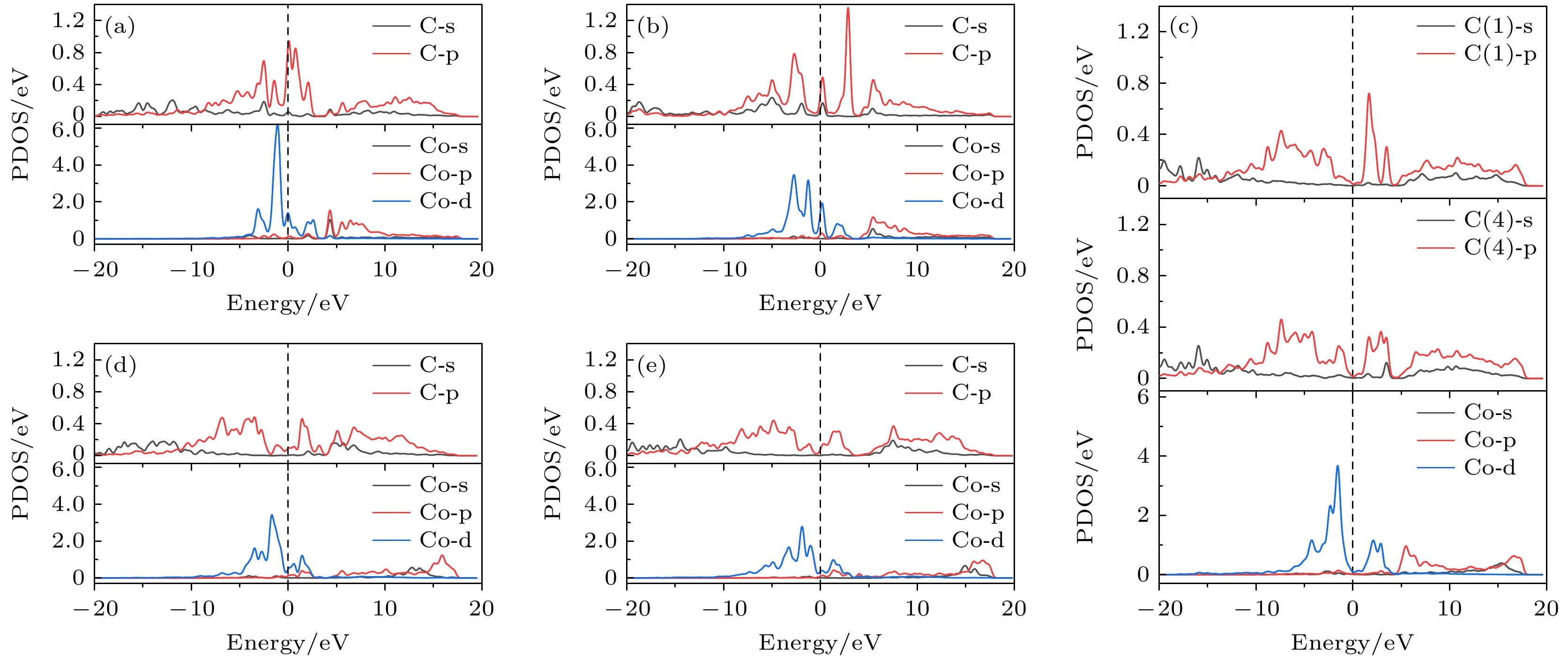
图 8 基底中Co与成键C原子的部分态密度图 (a) Co在第1层; (b) Co在第2层; (c) Co在第3层; (d) Co在第4层; (e) Co在第5层
Figure 8. Partial density of states of Co and bonded C atoms in the substrate: (a) Co atom doped in the first layer; (b) Co atom doped in the second layer; (c) Co atom doped in the third layer; (d) Co atom doped in the fourth layer; (e) Co atom doped in the fifth layer.
表 1 不同原子层数金刚石表面结构优化后的层间距变化
Table 1. Variation of layer spacing after structural optimization of diamond models with different numbers of atomic layers.
原子层数/N 层间距变化/% ${\varDelta _{12}}$ ${\varDelta _{23}}$ ${\varDelta _{34}}$ ${\varDelta _{45}}$ ${\varDelta _{56}}$ ${\varDelta _{67}}$ 3 –10.852 5 –11.142 4.606 7 –10.716 4.643 –0.429 9 –10.708 4.643 –0.701 0.933 11 –10.701 4.688 –0.702 0.825 0.472 13 –10.718 4.688 –0.704 0.862 0.330 –0.613 表 2 Co原子嵌入不同深度的孕镶金刚石基底/金刚石涂层界面结合能
Table 2. Interface binding energy of impregnated diamond substrates with Co atoms doped in different depths /diamond coating.
基底中
Co位置Eslab1
/eVEslab2
/eVEinterface
/eVA/Å2 Wad/
(J·m–2)表面第1层 –10822.680 –9874.157 –20740.528 56.903 12.302 表面第2层 –10824.324 –20739.004 11.410 表面第3层 –10820.914 –20725.527 8.575 表面第4层 –10816.048 –20735.417 12.730 表面第5层 –10816.702 –20738.245 13.342 不含Co –9879.266 –19801.206 13.454 表 3 Co位于第3层的原子布居数
Table 3. Atomic population when Co is doped in the third layer.
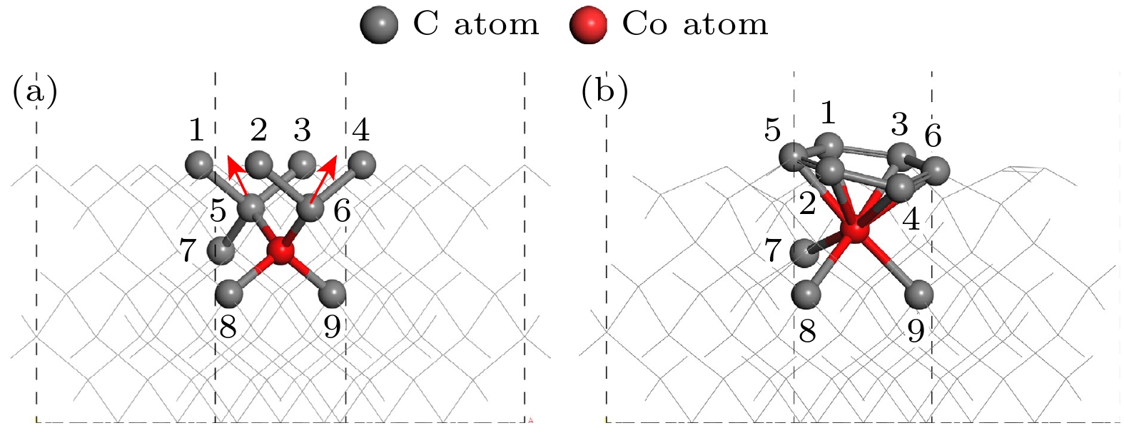
Atom Mulliken atomic populations Total electron/e Transfer charge/e s p d Co 0.05 –0.77 7.79 7.06 1.94 C(1) 1.32 2.82 0.00 4.14 –0.14 C(2) 1.19 2.91 0.00 4.10 –0.10 C(3) 1.22 2.94 0.00 4.15 –0.15 C(4) 1.18 3.00 0.00 4.17 –0.17 C(5) 1.22 2.94 0.00 4.15 –0.15 C(6) 1.18 2.91 0.00 4.10 –0.10 C(7) 1.22 2.90 0.00 4.12 –0.12 C(8) 1.17 3.04 0.00 4.20 –0.20 C(9) 1.17 3.04 0.00 4.20 –0.20 表 4 Co位于第3层的化学键布居数
Table 4. Bond population when Co is doped in the third layer.
Bond Population Length/Å Co—C(1) –0.22 1.94970 Co—C(2) –0.22 2.02913 Co—C(3) –0.31 1.93623 Co—C(4) –0.19 1.98079 Co—C(5) –0.13 1.93626 Co—C(6) –0.22 2.02911 Co—C(7) 0.41 2.07074 Co—C(8) 0.34 1.88913 Co—C(9) 0.34 1.88915 -
[1] Yan B, He N, Chen N, Weigold M, Chen H W, Sun S C, Wu Y, Fu S Y, Li L, Abele E 2025 Int. J. Extrem. Manuf. 7 015106
 Google Scholar
[2] Du Y F, Xie F M, Wang J, Xu B, Chen H Y, Yan B N, Wu Y J, Huang W F, Li H 2023 Materials 16 3640
 Google Scholar
[3] Wheeler D W, Wood R J K 2024 Wear 556–557 205488
 Google Scholar
[4] 简小刚, 张允华 2015 物理学报 64 046701
 Google Scholar
Jian X G, Zhang Y H 2015 Acta Phys. Sin. 64 046701
 Google Scholar
[5] Wang X L, Wu X, Lu K, Ye J W 2025 Diam. Relat. Mater. 152 111886.
 Google Scholar
[6] Liu X W, Zhang H, Lin G L, Wang Z G, Zhang J L, Shi H Y 2023 Vacuum 217 112562
 Google Scholar
[7] Tian Q Q, Huang N, Yang B, Zhuang H, Wang C, Zhai Z F, Li G H, Jia X Y, Liu L S, Jiang X 2017 J. Mater. Sci. Technol. 33 1097
 Google Scholar
[8] Li X J, He L L, Li Y S, Yang Q 2019 Surf. Coat. Technol. 360 20
 Google Scholar
[9] Saiki Y, Bando T, Harigai T, Takikawa Hirofumi, Hattori T, Sugita H, Kawahara, N, Tanaka K 2023 Diam. Relat. Mater. 132 109643
 Google Scholar
[10] Qiao Y, Nie S Y, Li W H, Liu E Z, Wang X C 2023 Appl. Surf. Sci. 633 157589
 Google Scholar
[11] Sedov V, Martyanov A, Ashkinazi E, Tiazhelov I, Savin S, Sovyk D, Mandal S, Fedorov S, Grigoriev S, Ralchenko V 2023 Surf. Interfaces 38 102861
 Google Scholar
[12] 简小刚, 陈军 2015 物理学报 64 216701
 Google Scholar
Jian X G, Chen J 2015 Acta Phys. Sin. 64 216701
 Google Scholar
[13] Sarangi S K, Chattopadhyay A, Chattopadhyay A K 2008 Appl. Surf. Sci. 254 3721
 Google Scholar
[14] Hu J B, Jian X G 2022 Mod. Phys. Lett. B 36 2250086
 Google Scholar
[15] 范舒瑜, 匡同春, 林松盛, 代明江 2023 材料导报 37 28
 Google Scholar
Fan S Y, Kuang T C, Lin S S, Dai M J 2023 Mater. Rep. 37 28
 Google Scholar
[16] Donnet J B, Paulmier D, Oulanti H 2004 Carbon 42 2215
 Google Scholar
[17] Lloret F, Soto B, Rouzbahani R, Gutiérrez M, Haenen K, Araujo D 2023 Diam. Relat. Mater. 133 109746
 Google Scholar
[18] Zhu P, Zhang Q, Xia Y X, Ma Y F, Gou H S, Liang X, Wu G H 2024 Mater. Today Phys. 48 101563
 Google Scholar
[19] Hu J B, Jian X G, Yang T, Peng X Y 2022 Diam. Relat. Mater. 123 108864
 Google Scholar
[20] Bi K, Liu J, Dai Q X 2012 Appl. Surf. Sci. 258 4581
 Google Scholar
[21] Pang X Z, Yang X Y, Yang J B, Zhao Y J, Pang M J 2021 Diam. Relat. Mater. 113 108297
 Google Scholar
[22] Ernzerhof M, Scuseria G E 1999 J. Chem. Phys. 110 5029
 Google Scholar
[23] Perdew J P, Burke K, Ernzerhof M 1996 Phys. Rev. Lett. 77 3865
 Google Scholar
[24] Chadi D J 1977 Phys. Rev. B 16 1746
 Google Scholar
[25] Jin S S, You Z Y, Han P D, Jiang A X, Sun C L, Wang L B, Zhang T, Liu S L 2024 Comput. Mater. Sci. 244 113235
 Google Scholar
Catalog
Metrics
- Abstract views: 1814
- PDF Downloads: 36
- Cited By: 0


 DownLoad:
