-
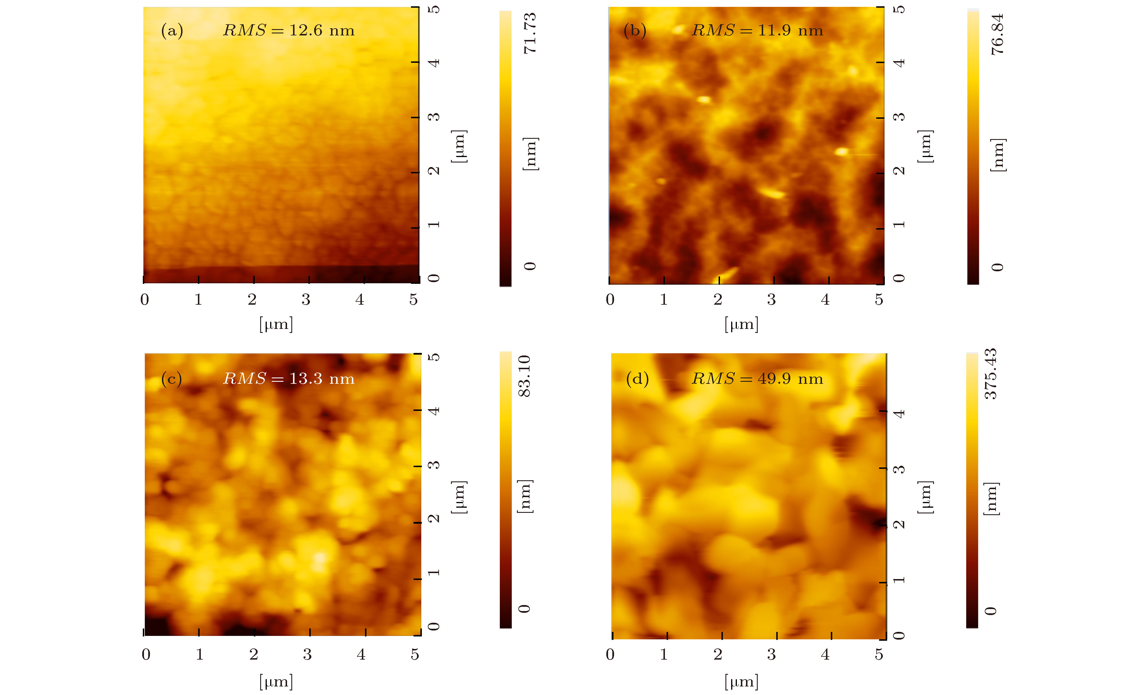
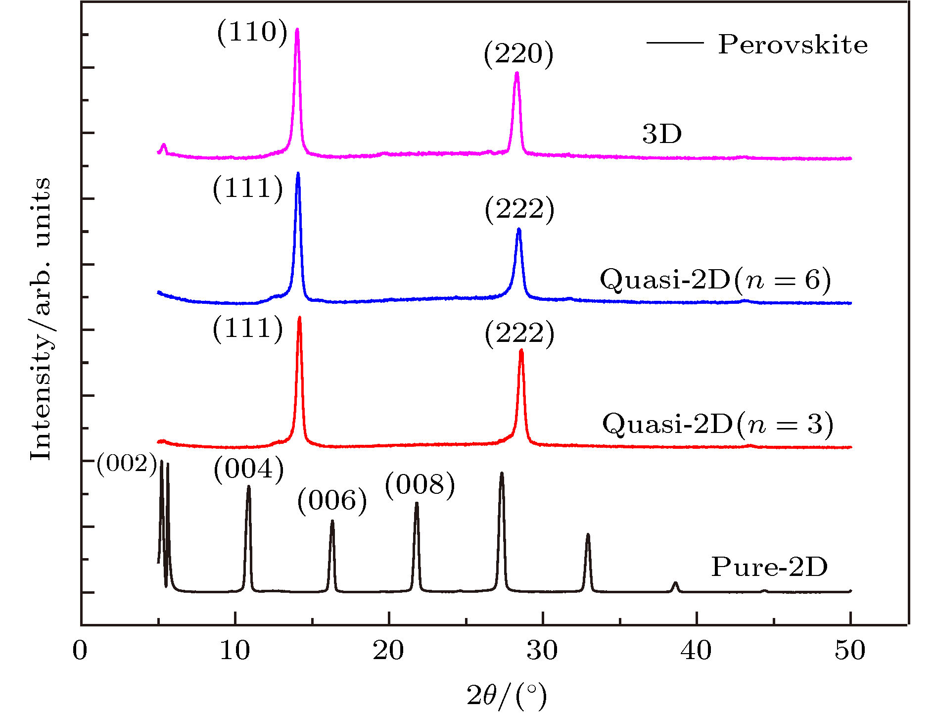
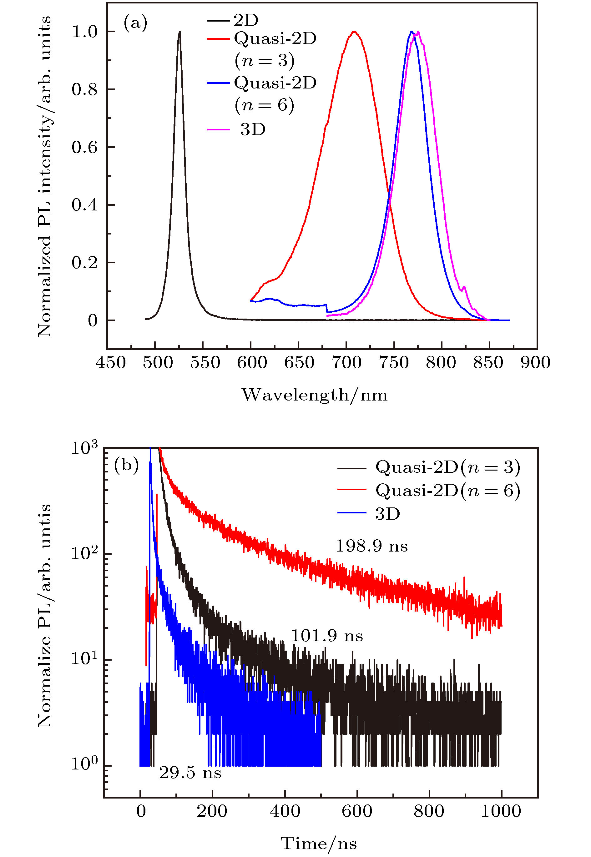
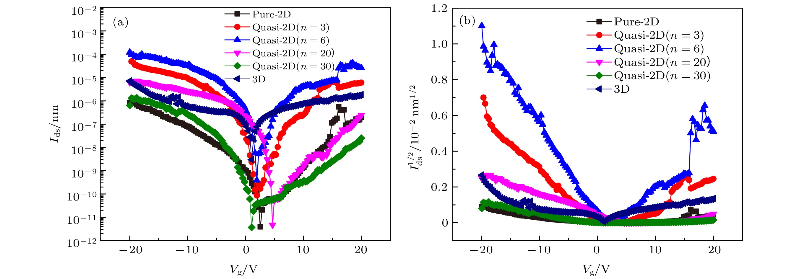
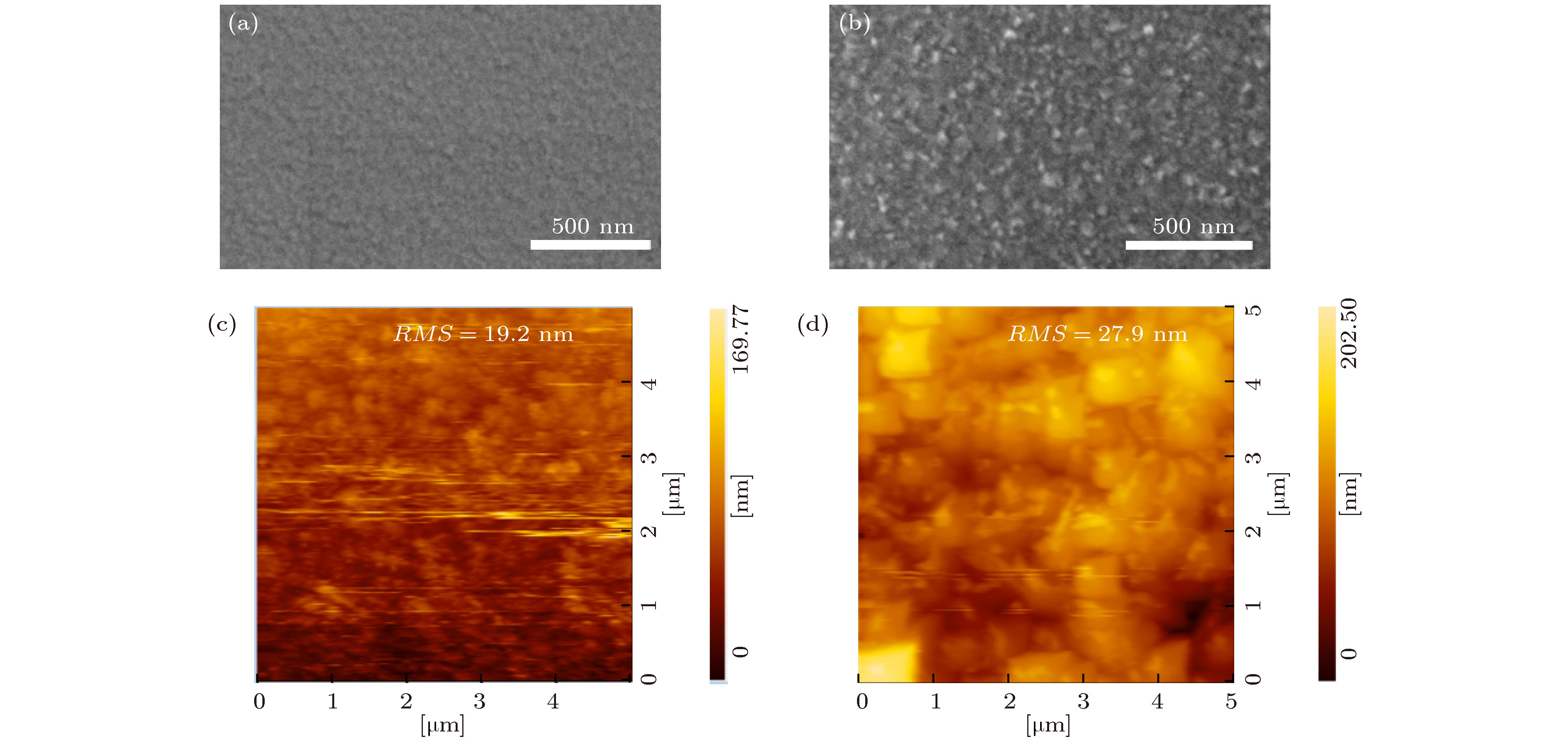
三维有机无机杂化钙钛矿因其优异的光电性能被视为光电领域极具前景的材料, 但其在湿度环境下的不稳定性成为制约产业化进程的关键因素之一. 本文采用一步溶液法成功制备了碘化铅基二维钙钛矿(PEA)2(MA)n–1PbnI3n + 1 (n = 1, 3 ,6, 20, 30), 对钙钛矿的维度及微观结构进行调控, 并将其应用作为薄膜晶体管(TFTs)器件的半导体沟道层. 实验结果表明, 独特的二维层状结构和量子约束效应有效地抑制了器件的环境不稳定性和离子迁移现象, TFTs器件性能得到提高. 基于准二维Quasi-2D (n = 6)钙钛矿的薄膜晶体管器件空穴迁移率(μhole)达到3.9 cm2/(V·s)、阈值电压为1.85 V、开关比高于104. 首次提出将准二维有机无机杂化钙钛矿材料应用到薄膜晶体管中, 为制备高性能、高稳定性的薄膜晶体管器件提供了新的思路.Despite the fact that three-dimensional organic-inorganic hybrid perovskite is regarded as a promising material in the field of optoelectronics and microelectronics due to its excellent photoelectric properties, however, the instability under the moisture environment and the gate-voltage screening effect associated with ionic transport are still serious, which restricts the development of perovskite devices. Here in this work, the lead iodide perovskite (PEA)2(MA)n–1PbnI3n+1 series are successfully prepared by one-step solution method, including pure-two-dimensional (pure-2D), quasi-two-dimensional (quasi-2D) and traditional three-dimensional (3D) perovskite materials. The dimension and microstructure of the perovskites are regulated, and the effects of dimensions on the performance of organic-inorganic hybrid perovskite materials are investigated firstly. The crystallization of the 2D perovskites and 3D perovskite films are observed obviously. Moreover, the surface of pure-2D perovskite film with discoid, regular and micron-sized grains is smoother than that of 3D perovskite film. And also, the unapparent grain boundary is exhibited in the quasi-2D perovskites. A uniform perovskite film with full coverage and inconspicuous grain boundaries facilitates the transmission capacity of the charge carriers in the channel layer due to the reduction of defects caused by the grain boundaries. And benefited from the high-quality films with inconspicuous grain boundary as demonstrated, the quasi-2D hybrid perovskite film exhibits a longer carrier lifetime (τns) than traditional 3D MAPbI3 perovskite film, revealing that the layered 2D structure is more favorable for carrier transport due to the fewer defects in it. In addition, under the condition of the same environment humidity, the 2D perovskite materials show better moisture stability. Then, to investigate the influences of dimensional structure on the perovskite field-effect devices, we fabricate the bottom-gate and top-contact thin film transistors (TFTs) based on the perovskite materials with different dimensions. As a result, the instability and ion migration effect for each of the devices are suppressed effectively due to the distinct 2D layer-structure and quantum confinement effect, which leads the device performance to be further improved. The device based on quasi-2D (n = 6) channel TFT achieves a hole mobility (μhole) of 3.9 cm2/(V·s), an on-off current ratio of 104 and more, and a 1.85V turn-on voltage of 1.85 V. The first application of quasi-2D organic and inorganic hybrid perovskite materials to thin film transistors provides a new idea for preparing the high-performance and stable thin film transistor devices.
-
Keywords:
- two-dimensional perovskite /
- environmental stability /
- thin film transistors /
- hole mobility
[1] Kojima A, Teshima K, Shirai Y, Miyasaka T 2009 J. Am. Chem. Soc. 131 6050
 Google Scholar
[2] Lee M M, Teuscher J, Miyasaka T, Murakami T N, Snaith H J 2012 Science 338 643
 Google Scholar
[3] Im J H, Jang I H, Pellet N, Grätzel M, Park N G 2014 Nat. Nanotechnol. 9 927
 Google Scholar
[4] Mei Y, Zhang C, Vardeny Z V, Jurchescu O D 2015 MRS Commun. 5 297
 Google Scholar
[5] Park C B, Kim K M, Lee J E, Na H I, Yoo S S, Yang M S 2014 Org. Electron. 15 3538
 Google Scholar
[6] Takeya J, Yamagishi M, Tominari Y, Nakazawa Y 2007 Solid-State Electron. 51 1338
 Google Scholar
[7] Robert F 2000 Science 287 415
 Google Scholar
[8] Chiarella F, Ferro P, Licci F, et al. 2007 Appl. Phys. A: Mater. Sci. Process. A86 89
 Google Scholar
[9] Feng L, Chun M, Hong W, Wei J H, Wei L Y, Arif D S, Tom W 2015 Nat. Commun. 6 8238
 Google Scholar
[10] Yusoff A R B M, Kim H P, Li X, Kim J, Jang J, Nazeeruddin M K 2017 Adv. Mater. 29 1602940
 Google Scholar
[11] Lin Y, Bai Y, Fang Y, Wang Q, Deng Y, Huang J 2017 ACS Energy Lett. 2 1571
 Google Scholar
[12] Chin X Y, Cortecchia D, Yin J, Bruno A, Soci C 2015 Nat. Commun. 6 7383
 Google Scholar
[13] Labram J G, Fabini D H, Perry E E, et al. 2015 J. Phys. Chem. Lett. 6 3565
 Google Scholar
[14] Smith I C, Hoke E T, Solis‐Ibarra D, McGehee M D, Karunadasa H I 2014 Angew. Chem. Int. Ed. 53 11232
 Google Scholar
[15] Cao D H, Stoumpos C C, Farha O K, Hupp J T, Kanatzidis M G 2015 J. Am. Chem. Soc. 137 7843
 Google Scholar
[16] Saparov B, Mitzi D B 2016 Chem. Rev. 116 4558
 Google Scholar
[17] Yang S, Niu W, Wang A L, Fan Z, Chen B, Tan C, Lu Q, Zhang H 2017 Angew. Chem. Int. Ed. 56 4252
 Google Scholar
[18] Wang Y, Liu X, Li L, Ji C, Sun Z, Han S, Tao K, Luo J 2019 Chem. Asian J. 14 1530
 Google Scholar
[19] Kagan C R, Mitzi D B, Dimitrakopoulos C D 1999 Science 286 945
 Google Scholar
[20] Matsushima T, Mathevet F, Heinrich B, et al. 2016 Appl. Phys. Lett. 109 253301
 Google Scholar
[21] Zhu H, Liu A, Luque H L, Sun H, Ji D, Noh Y Y 2019 Acs Nano. 13 3971
 Google Scholar
[22] Ahmad S, Fu P, Yu S, Yang Q, Liu X, Wang X, Wang X, Guo X, Li C 2019 Joule 3 794
 Google Scholar
[23] 陈皓然, 夏英东, 陈永华, 黄维 2018 材料导报 32 1
 Google Scholar
Chen H R, Xia Y D, Chen Y H, Huang W 2018 Materials Reports 32 1
 Google Scholar
[24] 张琦忠 2018 硕士学位论文 (合肥: 中国科学技术大学)
Zhang Q 2018 M. S. Thesis (Hefei: University of Science and Technology of China) (in Chinese)
[25] Tsai H, Nie W, Blancon J C, et al. 2016 Nature 536 312
 Google Scholar
[26] Cheng Z, Lin J 2010 Crystengcomm 12 2646
 Google Scholar
[27] Zhang F, Lu H, Tong J, Berry J J, Beard M C, Zhu K 2020 Energy Environ. Sci. 13 1154
 Google Scholar
[28] Zheng H, Liu G, Zhu L, Ye J, Zhang X, Alsaedi A, Hayat T, Pan X, Dai S 2018 Adv. Energy Mater. 8 1800051.1
[29] Peng Y, Tang L, Zhou Z, Xu J, Li J, Cai H, Ni J, Zhang J 2018 J. Phys. D: Appl. Phys. 51 445101
 Google Scholar
[30] Soe C M M, Nagabhushana G P, Shivaramaiah R, et al. 2018 Proc. Natl. Acad. Sci. 116 58
-
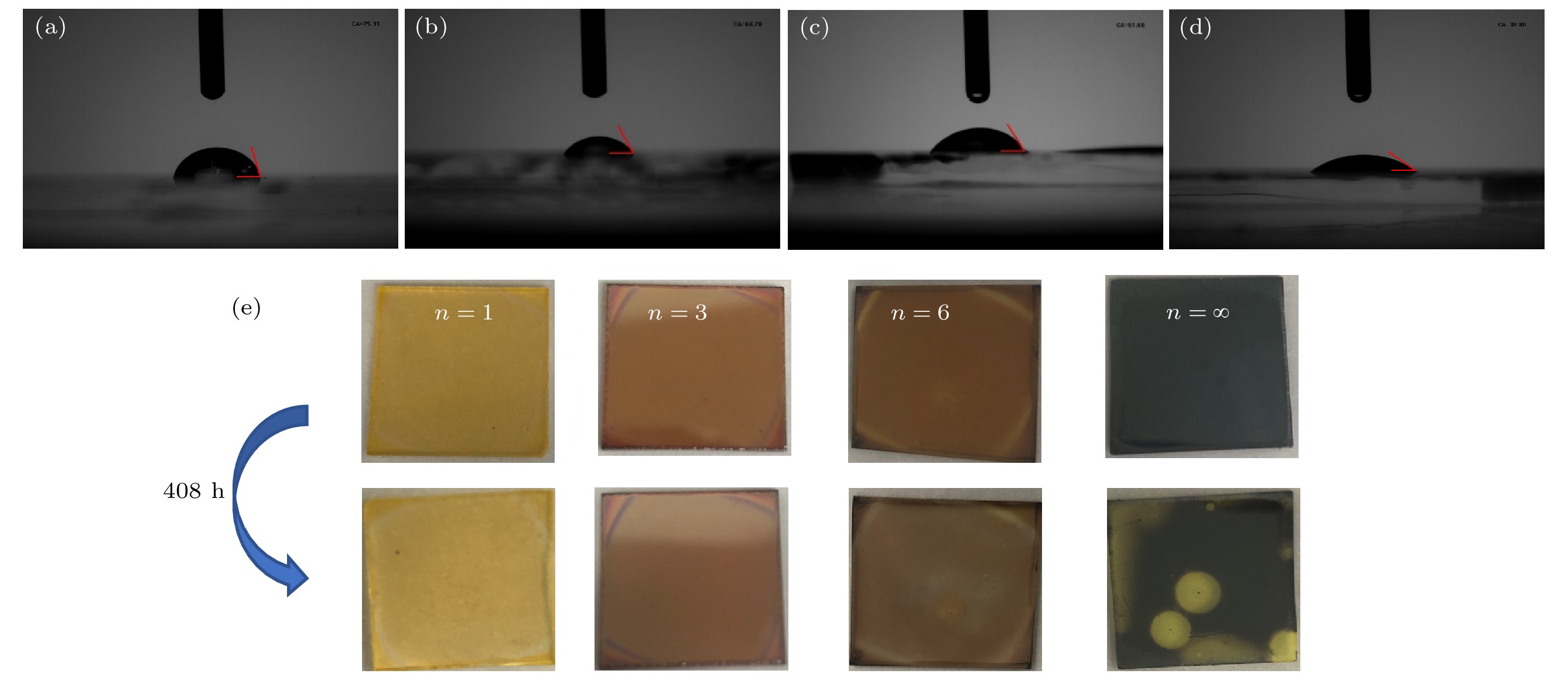
图 7 不同维度钙钛矿薄膜的水接触角 (a) 纯二维; (b) n = 3的准二维; (c) n = 6的准二维; (d) 三维钙钛矿; (e) 不同维度钙钛矿在30%湿度的空气环境下暴露前后对比图
Fig. 7. Water contact angle of perovskite films with different dimensions: (a) Pure-2D; (b) Quasi-2D (n = 3); (c) Quasi-2D (n = 6); (d) 3D; (e) images of perovskite films with different dimensions before and after exposed to 30% humidity of the ambient environment.
表 1 不同维度钙钛矿TRPL衰减曲线拟合的时间常数和振幅
Table 1. Time constant and amplitude of perovskites with different dimensions by fitting the TRPL decay curves.
PEA2MAn-1PbnI3 n+1 A1 τ1/ns A2 τ2/ns τave/ns n = 1 — — — — — n = 3 572.0 18.3 66.9 125.2 101.9 n = 6 520.9 31.2 306.2 236.6 198.9 n = ∞ 347.6 6.2 77.16 44.3 29.5 表 2 不同维度钙钛矿薄膜的水接触角
Table 2. Summary of water contact angle of perovskite films with different dimensions
Pure-2D Quasi-2D (n = 3) Quasi-2D (n = 6) 3D Water contact angle/(°) 75.31 64.70 61.66 38.88 表 3 基于不同维度钙钛矿的薄膜晶体管器件的相关性能参数
Table 3. Summary of related performance parameters of TFT devices based on the perovskite with different dimensions.
Perovskite
styleμhole/cm2·(V·s)–1 Ion/Ioff Vth/V SS/V·dec–1 Pure-2D 7.2×10⁻² 105 2.30 0.11 Quasi-2D
(n = 3)2.90 105 3.10 0.60 Quasi-2D
(n = 6)3.90 105 1.85 1.10 Quasi-2D
(n = 20)0.79 105 0.44 1.25 Quasi-2D
(n = 30)0.27 105 0.70 1.60 3D 0.30 104 0.60 0.14 -
[1] Kojima A, Teshima K, Shirai Y, Miyasaka T 2009 J. Am. Chem. Soc. 131 6050
 Google Scholar
[2] Lee M M, Teuscher J, Miyasaka T, Murakami T N, Snaith H J 2012 Science 338 643
 Google Scholar
[3] Im J H, Jang I H, Pellet N, Grätzel M, Park N G 2014 Nat. Nanotechnol. 9 927
 Google Scholar
[4] Mei Y, Zhang C, Vardeny Z V, Jurchescu O D 2015 MRS Commun. 5 297
 Google Scholar
[5] Park C B, Kim K M, Lee J E, Na H I, Yoo S S, Yang M S 2014 Org. Electron. 15 3538
 Google Scholar
[6] Takeya J, Yamagishi M, Tominari Y, Nakazawa Y 2007 Solid-State Electron. 51 1338
 Google Scholar
[7] Robert F 2000 Science 287 415
 Google Scholar
[8] Chiarella F, Ferro P, Licci F, et al. 2007 Appl. Phys. A: Mater. Sci. Process. A86 89
 Google Scholar
[9] Feng L, Chun M, Hong W, Wei J H, Wei L Y, Arif D S, Tom W 2015 Nat. Commun. 6 8238
 Google Scholar
[10] Yusoff A R B M, Kim H P, Li X, Kim J, Jang J, Nazeeruddin M K 2017 Adv. Mater. 29 1602940
 Google Scholar
[11] Lin Y, Bai Y, Fang Y, Wang Q, Deng Y, Huang J 2017 ACS Energy Lett. 2 1571
 Google Scholar
[12] Chin X Y, Cortecchia D, Yin J, Bruno A, Soci C 2015 Nat. Commun. 6 7383
 Google Scholar
[13] Labram J G, Fabini D H, Perry E E, et al. 2015 J. Phys. Chem. Lett. 6 3565
 Google Scholar
[14] Smith I C, Hoke E T, Solis‐Ibarra D, McGehee M D, Karunadasa H I 2014 Angew. Chem. Int. Ed. 53 11232
 Google Scholar
[15] Cao D H, Stoumpos C C, Farha O K, Hupp J T, Kanatzidis M G 2015 J. Am. Chem. Soc. 137 7843
 Google Scholar
[16] Saparov B, Mitzi D B 2016 Chem. Rev. 116 4558
 Google Scholar
[17] Yang S, Niu W, Wang A L, Fan Z, Chen B, Tan C, Lu Q, Zhang H 2017 Angew. Chem. Int. Ed. 56 4252
 Google Scholar
[18] Wang Y, Liu X, Li L, Ji C, Sun Z, Han S, Tao K, Luo J 2019 Chem. Asian J. 14 1530
 Google Scholar
[19] Kagan C R, Mitzi D B, Dimitrakopoulos C D 1999 Science 286 945
 Google Scholar
[20] Matsushima T, Mathevet F, Heinrich B, et al. 2016 Appl. Phys. Lett. 109 253301
 Google Scholar
[21] Zhu H, Liu A, Luque H L, Sun H, Ji D, Noh Y Y 2019 Acs Nano. 13 3971
 Google Scholar
[22] Ahmad S, Fu P, Yu S, Yang Q, Liu X, Wang X, Wang X, Guo X, Li C 2019 Joule 3 794
 Google Scholar
[23] 陈皓然, 夏英东, 陈永华, 黄维 2018 材料导报 32 1
 Google Scholar
Chen H R, Xia Y D, Chen Y H, Huang W 2018 Materials Reports 32 1
 Google Scholar
[24] 张琦忠 2018 硕士学位论文 (合肥: 中国科学技术大学)
Zhang Q 2018 M. S. Thesis (Hefei: University of Science and Technology of China) (in Chinese)
[25] Tsai H, Nie W, Blancon J C, et al. 2016 Nature 536 312
 Google Scholar
[26] Cheng Z, Lin J 2010 Crystengcomm 12 2646
 Google Scholar
[27] Zhang F, Lu H, Tong J, Berry J J, Beard M C, Zhu K 2020 Energy Environ. Sci. 13 1154
 Google Scholar
[28] Zheng H, Liu G, Zhu L, Ye J, Zhang X, Alsaedi A, Hayat T, Pan X, Dai S 2018 Adv. Energy Mater. 8 1800051.1
[29] Peng Y, Tang L, Zhou Z, Xu J, Li J, Cai H, Ni J, Zhang J 2018 J. Phys. D: Appl. Phys. 51 445101
 Google Scholar
[30] Soe C M M, Nagabhushana G P, Shivaramaiah R, et al. 2018 Proc. Natl. Acad. Sci. 116 58
计量
- 文章访问数: 12017
- PDF下载量: 257
- 被引次数: 0


 下载:
下载:


