


-
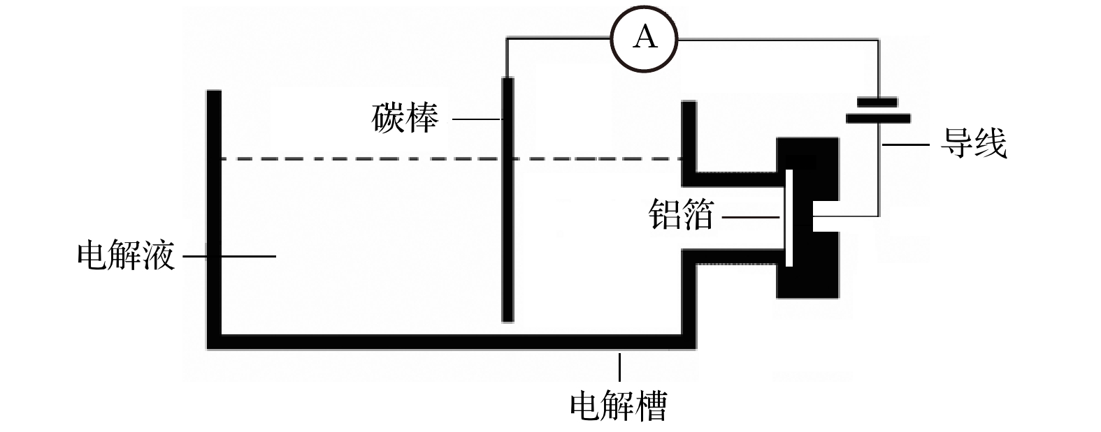
多孔氧化铝薄膜因其优异的介电、机械和光学性能, 广泛应用于电子器件、催化载体等领域. 阳极氧化是制备高质量多孔氧化铝薄膜的主要方法, 常用的碳棒对电极的导电行为和机制是影响薄膜微结构及其物性的一个重要因素. 本文选取质量分数为6%的磷酸为电解液, 圆形铝箔为阳极, 碳棒作为对电极, 电极间距为15 cm, 氧化时间为40 s, 实验研究了氧化电压在100—140 V下碳棒的导电行为. 实验结果显示, 氧化铝薄膜的孔洞深度和孔径由薄膜中心向外呈对称性递减分布. 当氧化电压低于110 V时, 制备的氧化铝薄膜孔深和孔径由薄膜中心向外渐变梯度较小, 宏观上呈现均一的结构色; 当氧化电压达到110 V时, 氧化铝薄膜孔深和孔径渐变梯度较大, 薄膜呈现虹彩环形的结构色, 随着氧化电压的增大, 薄膜孔深和孔径渐变梯度增加, 结构色环的数量增多, 可见光内色域宽度显著增大. 利用电磁学和电化学理论计算了碳棒在不同氧化电压下的导电行为并分析了其导电机制, 得到了碳棒具有“准点电极”导电特性的结论, 揭示了碳棒上点电极位置的选择遵循两极间的电阻最小原则. 这一发现不仅丰富了阳极氧化的电化学理论, 还为制备多功能的氧化铝薄膜提供了理论和实验支撑.Porous anodic aluminum oxide (AAO) films, due to their excellent dielectric, mechanical, and optical properties, have been widely used in electronic devices, catalytic supports, and optical materials. Anodization is the primary method for fabricating high-quality porous AAO films. The conductive behavior and mechanism of commonly used carbon rod counter electrodes are significant factors influencing the microstructure and properties of the films. In this study, a phosphoric acid solution with a mass fraction of 6% is used as the electrolyte, circular aluminum foil serves as the anode, and carbon rods are used as the counter electrodes spaced 15 cm apart. The oxidation time is fixed at 40 s. The conductive behaviors of the carbon rod under oxidation voltages ranging from 100 to 140 V are experimentally investigated. The results show that the pore depth and diameter of the AAO film symmetrically decrease from the film center toward the edges. When the oxidation voltage is below 110 V, the gradients of pore depth and diameter from the center outward are relatively small, resulting in a macroscopically uniform structural color. At an oxidation voltage of 110 V, the gradients of pore depth and diameter increase significantly, resulting in iridescent concentric ring structural colors. As the voltage increases further, the gradients become more pronounced, the number of structural color rings increases, and the visible color gamut significantly broadens. Electromagnetic and electrochemical theories are utilized to calculate the conductive behaviors of the carbon rod under different oxidation voltages and to analyze its conduction mechanism. The carbon rod is found to exhibit “quasi-point electrode” conductive characteristics, with the selection of point electrode positions on the carbon rod following the principle of minimizing the resistance between the two electrodes. This finding not only enriches the electrochemical theory of anodization but also provides theoretical and experimental support for fabricating multifunctional AAO films.
-
Keywords:
- porous anodic aluminum oxide /
- quasi-point electrode /
- current density gradient /
- structural color modulation
-
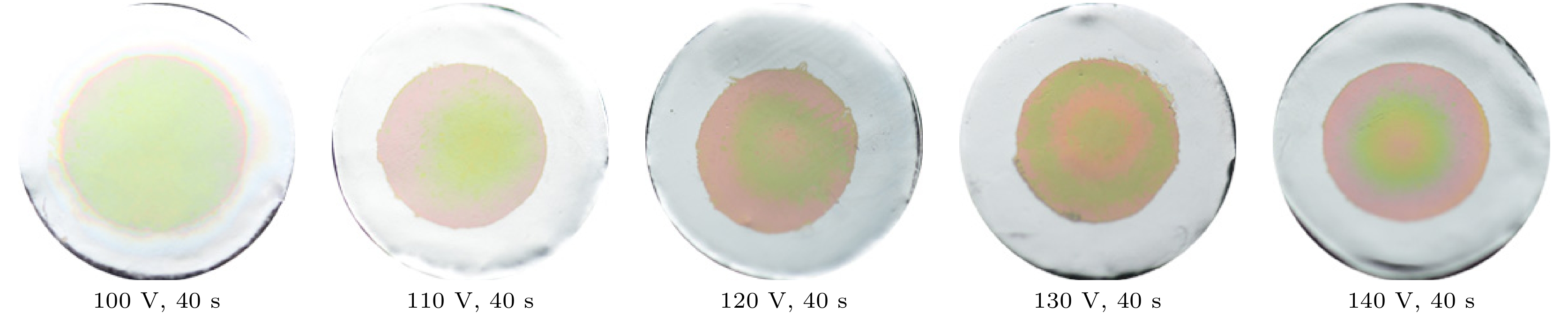
图 2 氧化电压分别为100, 110, 120, 130和140 V, 氧化时间均为40 s的薄膜数码照片
Fig. 2. Digital photographs of thin films prepared under conditions with oxidation voltages of 100, 110, 120, 130, and 140 V, and oxidation times of 40 seconds each.

图 3 (a)氧化电压大于110 V时电流线示意图; (b)AAO薄膜测试区域图
Fig. 3. (a) Current line diagram when the oxidation voltage is greater than 110 V; (b) AAO film test area map.
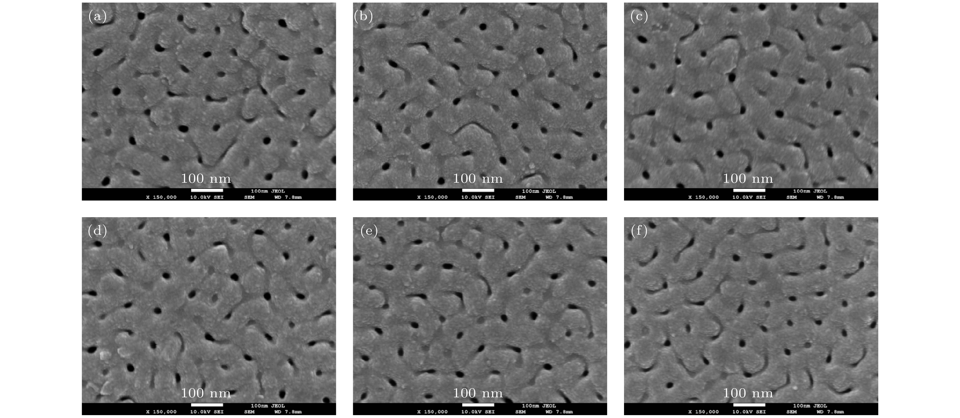
图 4 氧化电压140 V, 氧化时间40 s制备的AAO薄膜不同区域的SEM图 (a) 薄膜A区域; (b) 薄膜B区域; (c) 薄膜C区域; (d) 薄膜D区域; (e) 薄膜E区域; (f) 薄膜F区域
Fig. 4. Surface electron microscopic images of different regions of AAO films prepared at oxidation voltage of 140 V, oxidation time of 40 s: (a) Region A; (b) region B; (c) region C; (d) region D; (e) region E; (f) region F.
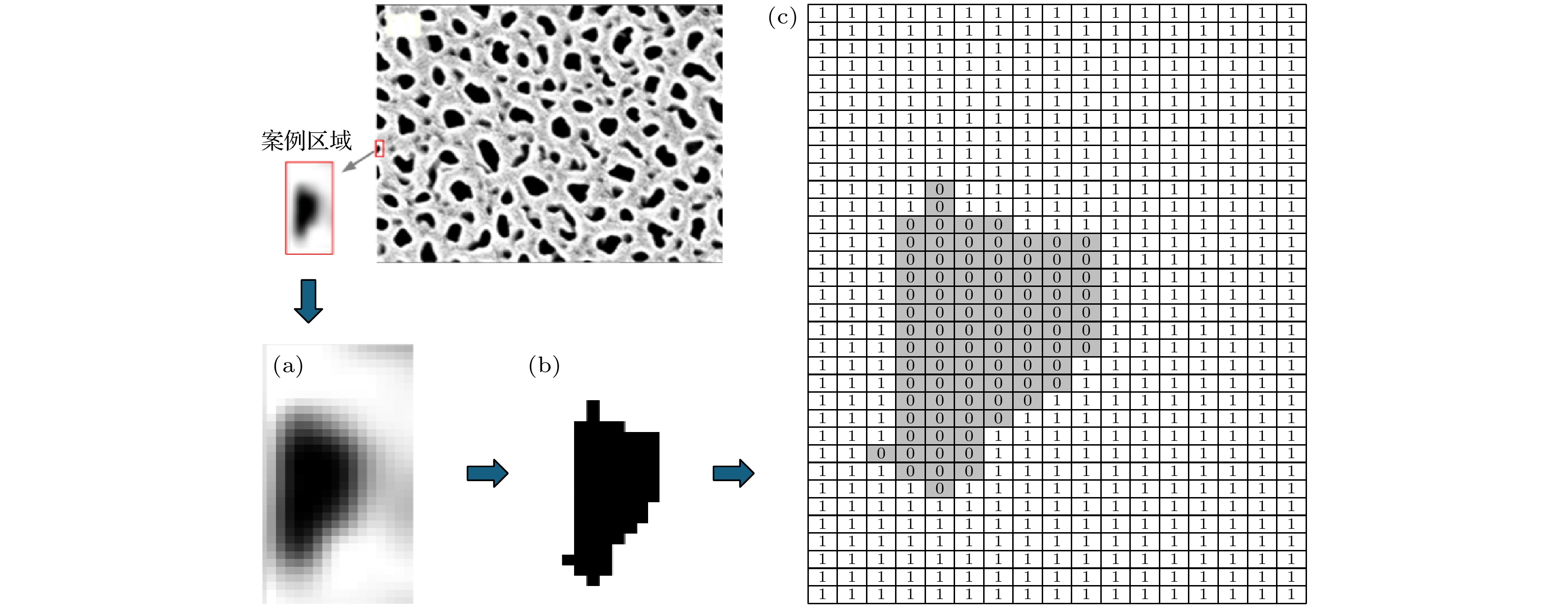
图 5 图像二值法计算AAO孔隙率示意图 (a) 先将图像二值化; (b) 阈值选择; (c) 面积计算
Fig. 5. Diagram illustrating the calculation of porosity of AAO using image binarization method: (a) Convert the image to a binary format; (b) threshold selection; (c) area calculation.
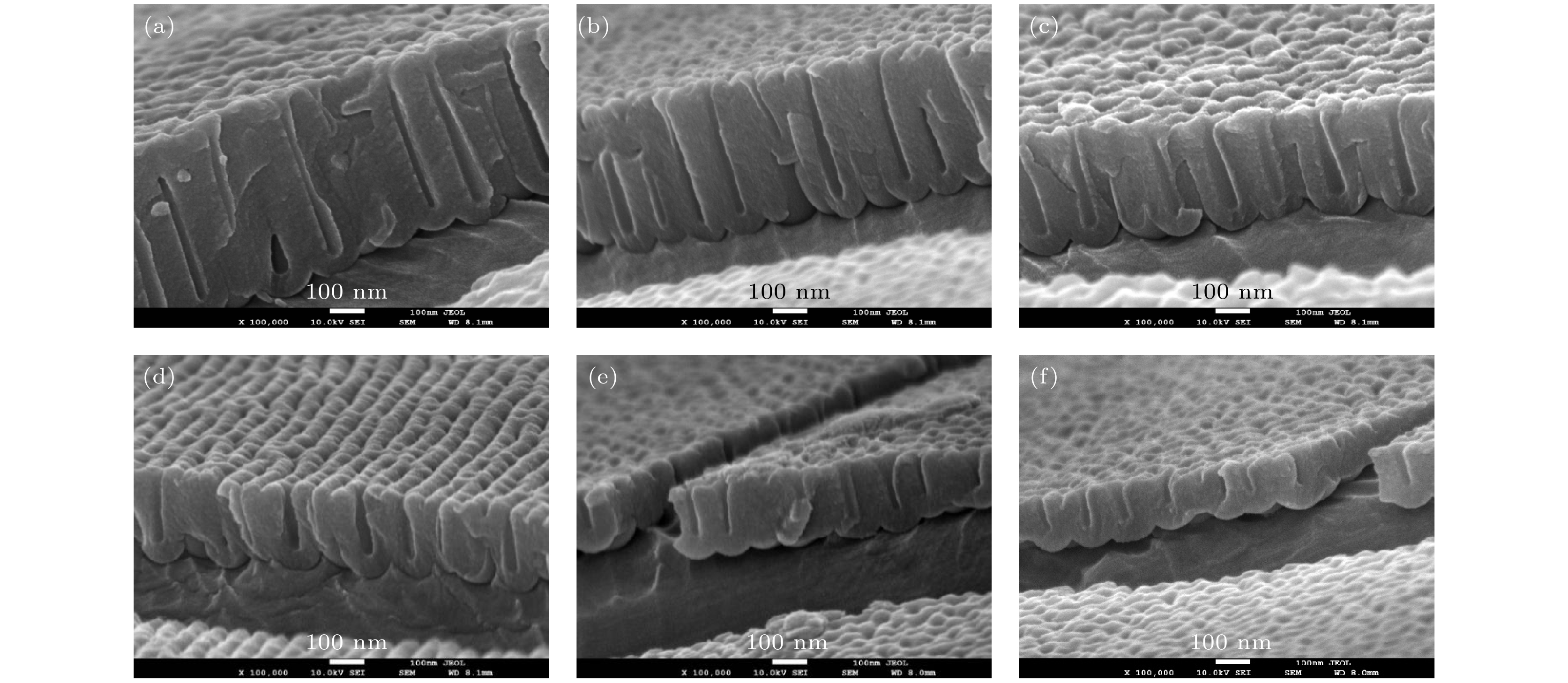
图 6 氧化电压140 V, 氧化时间40 s制备的AAO薄膜不同区域的SEM截面图 (a) 薄膜A区域; (b) 薄膜B区域; (c) 薄膜C区域; (d) 薄膜D区域; (e) 薄膜E区域; (f) 薄膜F区域
Fig. 6. Cross-sectional electron microscopy images of AAO films prepared at an oxidation voltage of 140 V and an oxidation time of 40 s, showing different regions: (a) Region A; (b) region B; (c) region C; (d) region D; (e) region E; (f) region F.

图 7 (a) AAO薄膜厚度截面示意图; (b) 100 V制备的AAO薄膜测试区域图
Fig. 7. (a)AAO film thickness cross-section diagram; (b)test area map of AAO film fabricated at 100 V.
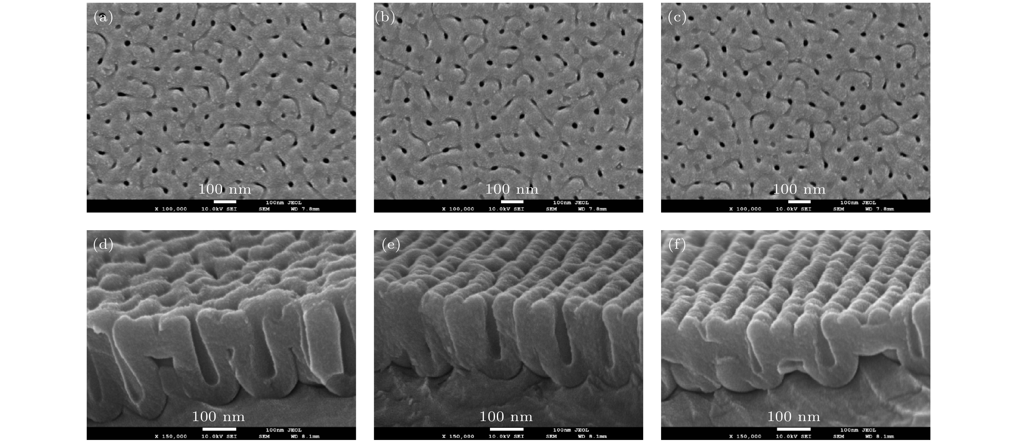
图 8 氧化电压100 V, 氧化时间40 s制备的AAO薄膜不同区域的SEM图 (a), (d) 薄膜A区域的表面和截面SEM照片; (b), (e) 薄膜B区域的表面和截面SEM照片; (c), (f) 薄膜C区域的表面和截面SEM照片
Fig. 8. SEM images of different regions of the AAO film prepared at an anodization voltage of 100 V and an anodization time of 40 s: (a), (d) Surface SEM image of region A in film; (b), (e) surface SEM image of region B in film; (c), (f) surface SEM image of region C in film.
图 9 氧化电压100 V时等效电流线示意图
Fig. 9. Equivalent current line diagram at an oxidation voltage of 100 V.
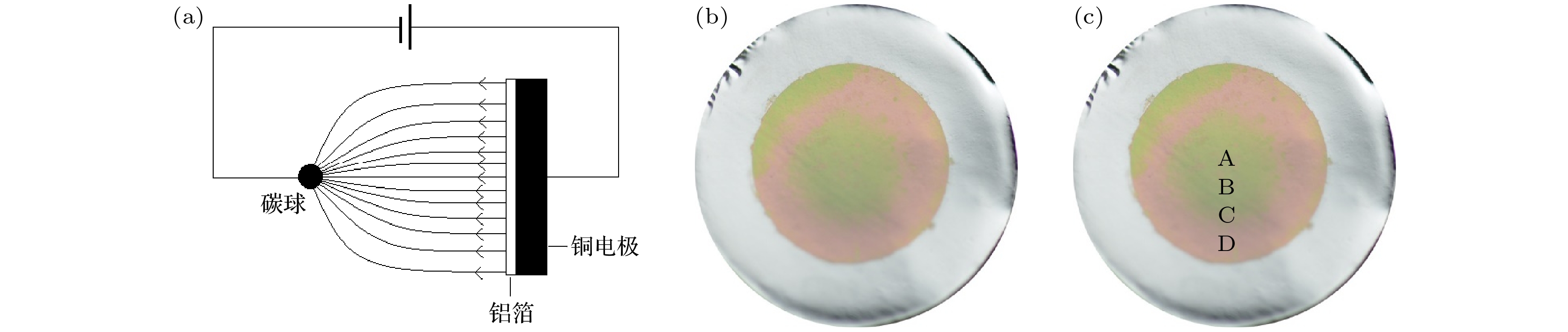
图 10 (a) 碳球点电极电流线示意图; (b) 碳球点电极、氧化电压30 V、氧化时间为4 min数码照片; (c) 碳球点电极、氧化电压30 V、氧化时间为4 min样品的测试区域
Fig. 10. (a) Schematic diagram of current lines for carbon sphere microelectrode; (b) digital photograph of carbon sphere microelectrode at an oxidation voltage of 30 V and oxidation time of 4 min; (c) test area of the sample with carbon sphere microelectrode at an oxidation voltage of 30 V and oxidation time of 4 min.
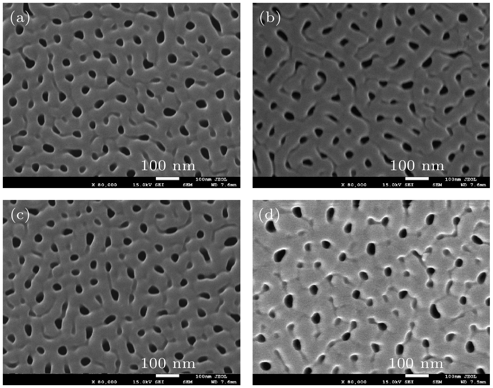
图 11 碳球点电极、氧化电压30 V, 氧化时间4 min制备的AAO薄膜不同区域的表面电镜图 (a) 区域A; (b) 区域B; (c) 区域C; (d) 区域D
Fig. 11. Surface SEM images of AAO films prepared with a carbon sphere point electrode, oxidation voltage of 30 V, and oxidation time of 4 min from different regions: (a) Region A; (b) region B; (c) region C; (d) region D.
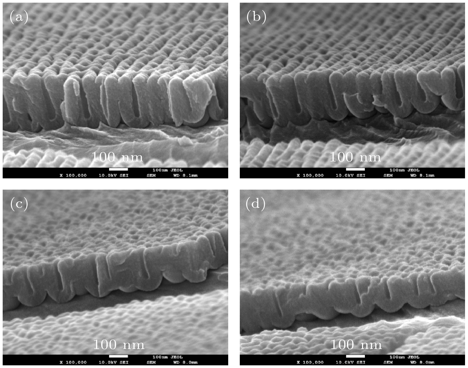
图 12 碳球点电极、氧化电压30 V, 氧化时间4 min制备的AAO薄膜不同区域的截面电镜图 (a) 区域A; (b) 区域B; (c) 区域C; (d) 区域D
Fig. 12. Cross-sectional SEM images of AAO films prepared with a carbon sphere point electrode, oxidation voltage of 30 V, and oxidation time of 4 min from different regions: (a) Region A; (b) region B; (c) region C; (d) region D.
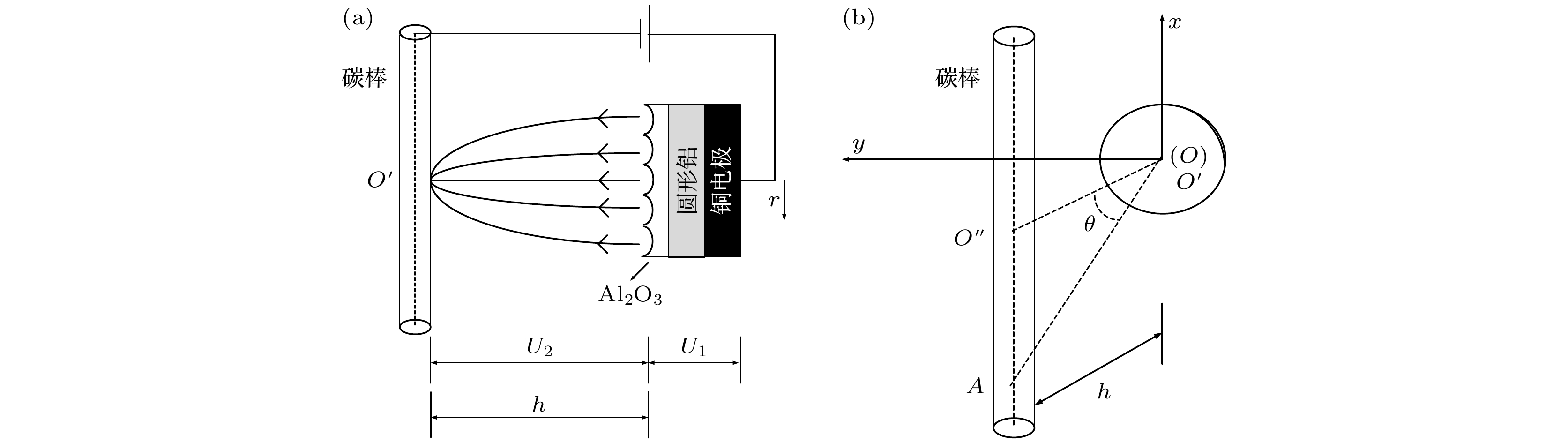
图 13 碳棒“准点电极”氧化示意图
Fig. 13. Schematic diagram of oxidation of carbon rod “quasi-point electrode”.
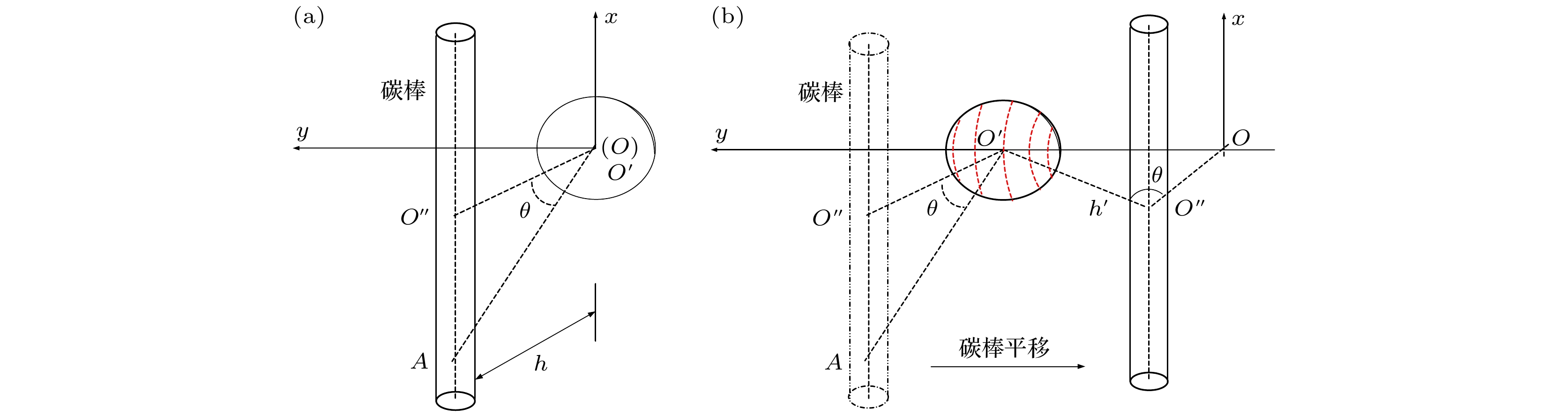
图 14 碳棒作为“准点电极”导电机理探讨示意图
Fig. 14. Schematic diagram for investigating the conduction mechanism of carbon rod as a "quasi-point electrode".
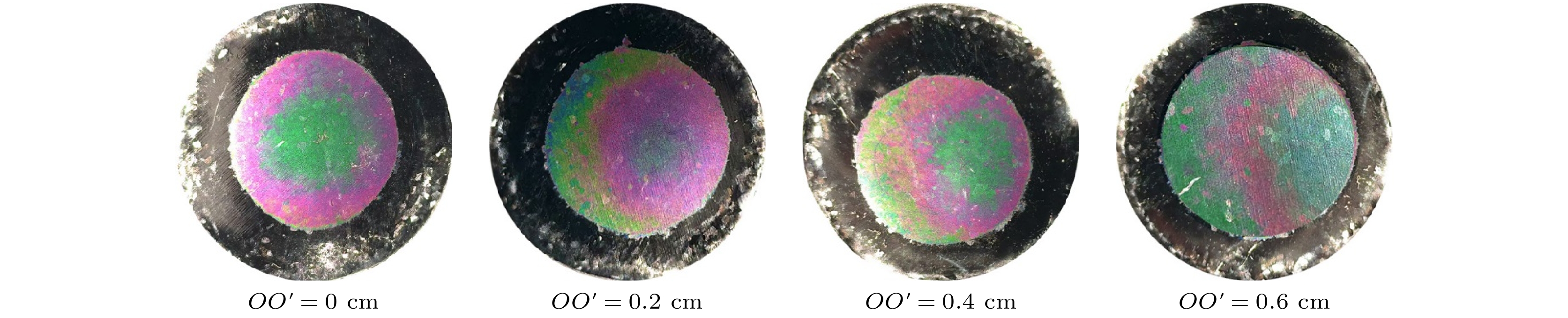
图 15 图14(b)中O与$ {O}^{\prime} $距离分别为0, 0.2, 0.4和0.6 cm, 氧化电压为110 V, 氧化时间为40 s条件下制备的AAO薄膜数码照片
Fig. 15. In Fig.14(b) shows digital photographs of AAO films prepared under an oxidation voltage of 110 V and an oxidation time of 40 s, with O-to-$ {O}^{\prime} $ distances of 0, 0.2, 0.4, and 0.6 cm, respectively.
表 1 氧化电压140 V, 氧化时间40 s的氧化铝薄膜测量参数和计算数据
Table 1. Measurement parameters and calculation data of alumina film with oxidation voltage of 140 V, oxidation time of 40 s.
区域 A B C D E F 孔隙率 0.0463 0.0457 0.0448 0.0426 0.0418 0.0377 薄膜厚度/nm 550 458 386 250 220 178 有效折射率 1.62 干涉级别/m 2 2 2 1 1 1 反射波长/nm 713 594 500 540 475 385 对应颜色 红色 黄色 绿色 绿色 蓝色 紫色  下载: 导出CSV
表 2 氧化电压100 V, 氧化时间40 s的氧化铝薄膜测量参数和计算数据
Table 2. Measurement parameters and calculation data of alumina film with oxidation voltage of 100 V, oxidation time of 40 s.
区域 A B C 平均孔半径/nm 10 9.5 9 孔隙率 0.0425 0.0410 0.0382 薄膜厚度/nm 264 254 230 有效折射率 1.62 1.62 1.62 干涉级别/m 1 1 1 反射波长/nm 570 549 497 对应颜色 绿色 绿色 绿色
下载: 导出CSV
表 3 碳球点电极、氧化电压30 V, 氧化时间4 min的氧化铝薄膜测量参数和计算数据
Table 3. Measurement parameters and calculation data for the aluminum oxide film with carbon sphere point electrode, oxidation voltage of 30 V, and oxidation time of 4 min.
区域 A B C D 平均孔径/nm 33 30 28 26 平均孔间距/nm 97 97 100 105 孔隙率 0.127 0.106 0.093 0.061 薄膜厚度/nm 300 263 226 190 有效折射率 1.57 1.58 1.59 1.61 干涉级别/m 1 1 1 1 反射波长/nm 628 554 479 408 对应颜色 红色 绿色 蓝色 紫色
下载: 导出CSV
表 4 碳棒平移不同位置氧化电流对应表
Table 4. Table of oxidation currents corresponding to different lateral positions of the carbon rod.
下载: 导出CSV
-
[1] Kushnir S E, Napolskii K S 2018 Mater. Des. 144 140
 Google Scholar
[2] Liu S X, Tian J L, Zhang W 2021 Nanotechnology 32 222001
Google Scholar
[3] Amouzadeh Tabrizi M, Ferré-Borrull J, Marsal L F 2020 Microchim. Acta 187 230
Google Scholar
[4] Dolbik A V, Sasinovich D A, Zavadskii S M, Golosov D A, Meledina M V, Rabatuev G G, Lazarouk S K 2025 Surf. Eng. Appl. Electrochem. 61 333
Google Scholar
[5] Acosta L K, Law C S, Santos A, Ferré-Borrull J, Marsal L F 2022 APL Photonics 7 026108
Google Scholar
[6] Ruiz-Clavijo A, Caballero-Calero O, Martín-González M 2021 Nanoscale 13 2227
Google Scholar
[7] Pappas J M, Thakur A R, Dong X Y 2020 Mater. Des. 192 108711
Google Scholar
[8] Szwachta G, Januszewska B, Włodarski M, Norek M 2023 Appl. Surf. Sci. 607 155031
Google Scholar
[9] Li P Z, Zhang Y, Zhang J Z, Liu L, Wang S, Liu R, Song Y, Zhu X F 2024 Trans. Nonferrous Met. Soc. China 34 2918
Google Scholar
[10] Sun X D, Guo X, Zhang J H, Wu J, Shi Y, Sun H Y, Pan C F, Pan L J 2024 Rare Met. 43 5410
Google Scholar
[11] He C Y, Qin L Y, Zhang S Y, Chen B Y, Zhu J Q, Lin F, Zhu X F 2024 Ceram. Int. 50 30906
Google Scholar
[12] 岂云开, 杨淑敏, 李欣, 徐芹, 顾建军 2022 物理学报 71 017801
Google Scholar
Qi Y K, Yang S M, Li X, Xu Q, Gu J J 2022 Acta Phys. Sin. 71 017801
Google Scholar
[13] Evertsson J, Vinogradov N A, Harlow G S, Carlà F, McKibbin S R, Rullik L, Linpé W, Felici R, Lundgren E 2018 RSC Adv. 8 18980
Google Scholar
[14] Kim B, Youn Y, Park Y S, Moon D N, Kang K, Han S, Lee J S 2016 Scr. Mater. 122 102
Google Scholar
[15] Roslyakov I V, Gordeeva E O, Napolskii K S 2017 Electrochim. Acta 241 362
Google Scholar
[16] Białek E, Włodarski M, Norek M 2020 Materials 13 3185
Google Scholar
[17] Kant K, Low K S, Marshal A, Shapter J G, Losic D, 2010 Appl. Mater. 2 3447
Google Scholar
[18] 杨淑敏, 韩伟, 顾建军, 李海涛, 岂云开 2015 物理学报 64 076102
Google Scholar
Yang S M, Han W, Gu J J, Li H T, Qi Y K 2015 Acta Phys. Sin. 64 076102
Google Scholar
[19] Yang S M, Wang A, Lin X M, Qi Y K, Shi G C, Han W, Gu J J 2024 Crystals 14 1102
Google Scholar
[20] Yang S M, Wang A, Li X, Shi G C, Qi Y K, Gu J J 2022 Molecules 27 4932
Google Scholar
[21] Brzózka A, Brudzisz A, Jeleń A, Kozak M, Wesół J, Iwaniec M, Sulka G D 2021 Mater. Sci. Eng. , B 263 114801
Google Scholar
[22] Li X Q, Wang J H, Fu Z Y, Dai G M, Tang Y, Chu F, Hou T, Wang Y, Song Y 2025 Chem. Select 10 e202500507
[23] 李国栋, 王倩, 邓保霞, 张雅晶 2014 物理学报 63 247802
Google Scholar
Li G D, Wang Q, Deng B X, Zhang Y J 2014 Acta Phys. Sin. 63 247802
Google Scholar
[24] 邱宇, 欧阳敏, 胡斌, 杨文博, 盖永浩, 邓聪, 张文祥 2023 吉林大学学报(信息科学版) 41 952
Qiu Y, Ouyang M, Hu B, Yang W B, Gai Y H, Deng C, Zhang W X 2023 J. f Jilin Univ. (Inf. Sci. Ed. ) 41 952
[25] Thompson G E, Wood G C 1983 Academic Press 23 269

 下载:
下载:
计量
- 文章访问数: 165
- PDF下载量: 5
- 被引次数: 0
