


-
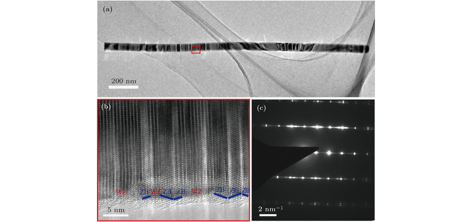
采用分子束外延技术在N-型Si (111)衬底上利用自催化生长机制外延砷化镓(GaAs)纳米线, 对生长的纳米线进行扫描电子显微镜测试, 纳米线垂直度高, 长度直径均匀度好. 对纳米线进行光致发光(photoluminescence, PL)光谱测试, 发现低温10 K下两个发光峰P1和P2分别位于1.493 eV和1.516 eV, 推断可能是纤锌矿/闪锌矿(WZ/ZB)混相结构引起的发光以及激子复合引起的发光; 随着温度升高, 发现两峰出现红移, 并通过Varshni公式拟合得到变温变化曲线. 对纳米线进行变功率PL光谱测试, 发现P1位置的峰位随功率增加而蓝移, 而P2位置的峰位不变. 通过拟合发现P1峰位与功率1/3次方成线性相关, 判断可能是WZ/ZB混相结构引起的Ⅱ型发光; 同时, 对P2位置的峰位进行拟合, P2为激子复合发光. 对纳米线进行拉曼光谱测试, 从光谱图中发现GaAs WZ结构特有的E2声子峰, 因此证明生长出的纳米线为WZ/ZB混相结构, 并通过高分辨透射电子显微镜更直观地观察到纳米线的混相结构.
-
关键词:
- GaAs纳米线 /
- 纤锌矿/闪锌矿混相结构 /
- 光致发光光谱 /
- 拉曼光谱
Gallium arsenide (GaAs) nanowires are epitaxially grown on an N-type Si (111) substrate by molecular beam epitaxy according to self-catalysis growth mechanism. Testing the grown nanowires by scanning electron microscope, it is found that the nanowires have high verticality and good uniformity in length and diameter. Variable temperature photoluminescence (PL) spectroscopy is used on nanowires. The test results show that the two luminescence peaks P1 and P2 at 10 K are located at 1.493 eV and 1.516 eV, respectively, and it is inferred that it may be the luminescence caused by WZ/ZB miscible structure and the free exciton luminescence peak. These two peaks present red-shift with temperature increasing. The temperature change curve is obtained by fitting the Varshni formula. The variable power PL spectroscopy test finds that the peak position of P1 position is blue shifted with power increasing, but the peak position of the P2 remains unchanged. By fitting, it is found that the P1 peak position is linearly related to power to the power of 1/3, and it is judged that it may be type-II luminescence caused by WZ/ZB mixed phase structure. At the same time, the peak position of the P2 position is fitted and parameter α approximately equals 1.56, therefore P2 is a free exciton luminescence. A Raman spectrum test is performed on the nanowires, and an E2 phonon peak unique to the GaAs WZ structure is found from the spectrum. It is proved that the grown nanowires possess WZ/ZB mixed phase structures, and the hybrid phase structure of nanowires is more intuitively observed by high resolution transmission electron microscopy.-
Keywords:
- GaAs nanowires /
- wurtzite/zincblende mixed phase structure /
- photoluminescence spectra /
- Raman spectra
[1] Dai X, Zhang S, Wang Z L, Adamo G, Liu H, Huang Y Z, Couteau C, Soci C 2014 Nano Lett. 14 2688
 Google Scholar
[2] Farrell A C, Senanayake P, Meng X, Hsieh N Y, Huffaker D L 2017 Nano Lett. 17 2420
Google Scholar
[3] Cammi D, Rodiek B, Zimmermann K, Kück S, Voss T 2017 J. Mater. Res. 32 2464
Google Scholar
[4] Tchernycheva M, Lavenus P, Zhang H, Babichev A V, Jacopin G, Shahmohammadi M, Julien F H, Ciechonski R, Vescovi G, Kryliouk O 2014 Nano Lett. 14 2456
Google Scholar
[5] Hussain L, Karimi M, Berg A, Jain V, Borgström M T, Gustafsson A, Samuelson L, Pettersson H 2017 Nanotechnology 28 485205
Google Scholar
[6] Ullah A R, Meyer F, Gluschke J G, Naureen S, Caroff P, Krogstrup P, Nygård J, Micolich A P 2018 Nano Lett. 18 5673
Google Scholar
[7] Price A, Martinez A 2015 J. Appl. Phys. 117 164501
Google Scholar
[8] Yang W, Pan D, Shen R, Wang X, Zhao J, Chen Q 2018 Nanotechnology 29 415230
[9] 毛宏伟, 刘一先, 李富铭 1990 中国激光 17 538
Google Scholar
Mao H W, Liu Y X, Li F M 1990 Chin. J. Las. 17 538
Google Scholar
[10] Han N, Wang F, Hou J J, Yip S, Lin H, Fang M, Xiu F, Shi X L, Hung T F, Ho J C 2012 Cryst. Growth Des. 12 6243
Google Scholar
[11] 夏宁, 方铉, 容天宇, 王登魁, 房丹, 唐吉龙, 王新伟, 王晓华, 李永峰, 姚斌, 魏志鹏 2018 中国激光 45 0603002
Xia N, Fang X, Rong T Y, Wang D K, Fang D, Tang J L, Wang X W, Wang X H, Li Y F, Yao B, Wei Z P 2018 Chin. J. Las. 45 0603002
[12] Glas F, Harmand J C, Patriarche G 2007 Phys. Rev. Lett. 99 146101
Google Scholar
[13] Hoang T B, Zhou H, Moses A F, Dheeraj D L, Helvoor A, Fimland B O, Weman H 2009 Mater. Res. Soc. Symp. Proc. 1144
[14] Vainorius N, Jacobsson D, Lehmann S, Gustafsson A, Dick K A, Samuelson L, Pistol M E 2014 Phys. Rev. B 89 165423
Google Scholar
[15] Kinzel J B, Schülein F J, Weiß M, Janker L, Bühler D D, Heigl M, Rudolph D, Morkötter S, Döblinger M, Bichler M, Abstreiter G, Finley J J, Wixforth A, Koblmüller G, Abstreiter G 2016 ACS Nano 10 4942
Google Scholar
[16] Senichev A, Corfdir P, Brandt O, Ramsteiner M, Breuer S, Schilling J, Geelhaar L, Werner P 2018 Nano Res. 1 14
[17] Mukherjee A, Ghosh S, Breuer S, Jahn U, Geelhaar L, Grahn H T 2017 J. Appl. Phys. 117 054308
[18] Kim H, Ren D, Farrell A C, Huffaker D L 2018 Nanotechnology 29 085601
Google Scholar
[19] 崔建功, 张霞, 颜鑫, 李军帅, 黄永清, 任晓敏 2014 物理学报 63 136103
Google Scholar
Cui J G, Zhang X, Yan X, Li J S, Huang Y Q, Ren X M 2014 Acta Phys. Sin. 63 136103
Google Scholar
[20] Liu Y, Peng Y, Guo J, La D, Xu Z 2018 AIP Adv. 8 055108
Google Scholar
[21] Zhou C, Zheng K, Liao Z M, Chen P P, Lu W, Zou J 2017 J. Mater. Chem. C 5 5257
Google Scholar
[22] Timofeeva M, Bouravleuv A, Cirlin G, Shtrom I, Soshnikov I, Reig Escalé M, Sergeyev A Grange R 2016 Nano Lett. 16 6290
Google Scholar
[23] Bussone G, Schäfer-Eberwein H, Dimakis E, Biermanns A, Carbone D, Tahraoui A, Geelhaar L, Bolívar P H, Schülli T U, Pietsch U 2015 Nano Lett. 15 981
Google Scholar
[24] Fontcuberta i Morral A, Colombo C, Abstreiter G, Arbiol J, Morante J R 2008 Appl. Phys. Lett. 92 063112
Google Scholar
[25] Bauer B, Rudolph A, Soda M, Fontcuberta i Morral A, Zweck J, Schuh D, Reiger E 2010 Nanotechnology 21 435601
Google Scholar
[26] Ramsteiner M, Brandt O, Kusch P, Breuer S, Reich S, Geelhaar L 2013 Appl. Phys. Lett. 103 043121
Google Scholar
[27] Jahn U, Lähnemann J, Pfüller C, Brandt O, Breuer S, Jenichen B, Ramsteiner M, Geelhaar L, Riechert H 2012 Phys. Rev. B 85 045323
Google Scholar
[28] Falcão B P, Leitão J P, Correia M R, Soares M R, Morales F M, Mánuel J M, Garcia R, Gustafsson A, Moreira M V B, de Oliveira A G, González J C 2013 J. Appl. Phys. 114 183508
Google Scholar
[29] Rudolph D, Schweickert L, Morkötter S, Loitsch B, Hertenberger S, Becker J, Bichler M, Abstreiter G, Finley J J, Koblmüller G 2013 Appl. Phys. Lett. 105 033111
[30] Varshni Y P 1967 Physica 34 149
Google Scholar
[31] Chiu Y S, Ya M H, Su W S, Chen Y F 2002 J. Appl. Phys. 92 5810
Google Scholar
[32] Jin S, Zheng Y, Li A 1997 J. Appl. Phys. 82 3870
Google Scholar
[33] Fang X, Wei Z P, Chen R, Tang J L, Zhao H F, Zhang L G, Zhao D X, Fang D, Li J H, Fang F, Chu X Y, Wang X H 2015 ACS Appl. Mater. Inter. 7 10331
Google Scholar
[34] Begum N, Piccin M, Jabeen F, Bais G, Rubini S, Martelli F, Bhatti A S 2008 J. Appl. Phys. 104 104311
Google Scholar
[35] Spirkoska D, Arbiol J, Gustafsson A, Conesa-Boj S, Glas F, Zardo I, Heigoldt M, Gass M H, Bleloch A L, Estrade S, Kaniber M, Rossler J, Peiro F, Morante J R, Abstreiter G, Samuelson L, Fontcuberta i Morral A 2009 Phys. Rev. B 80 245325
Google Scholar
-
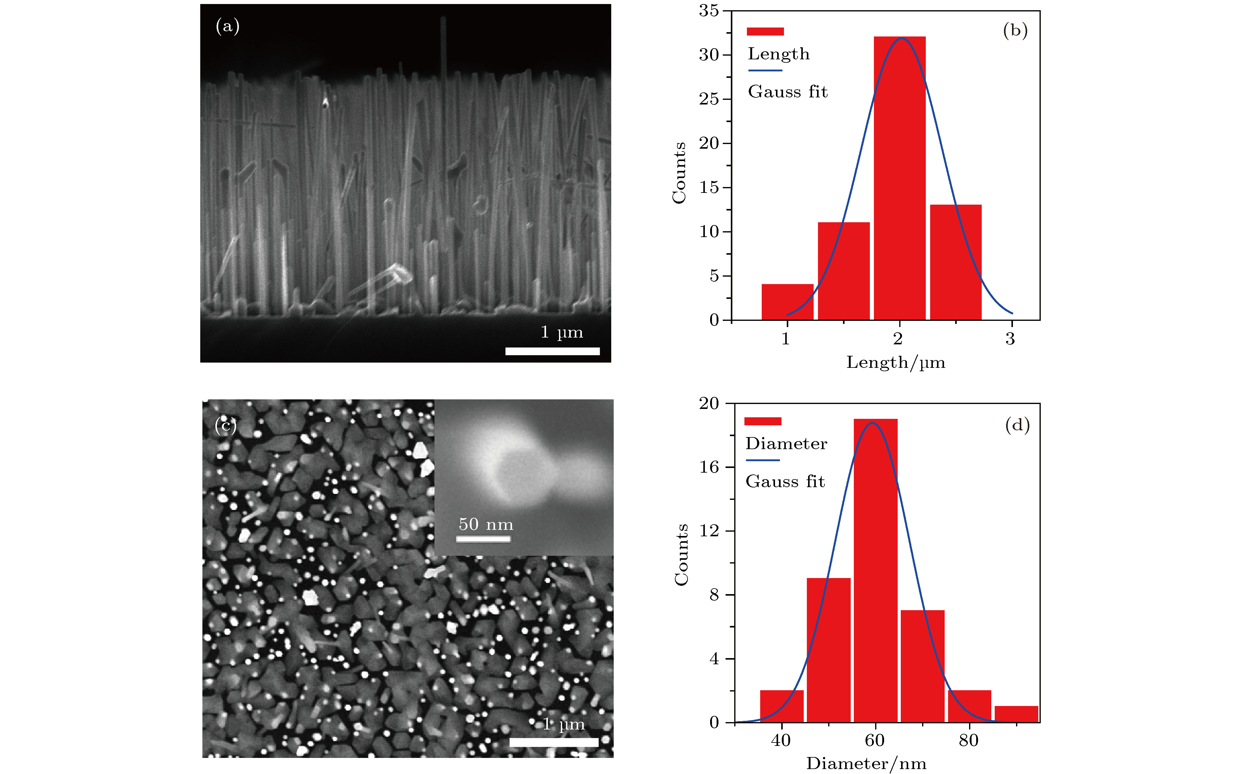
图 1 GaAs纳米线形貌及纳米线长度直径分布 (a) GaAs纳米线侧面SEM图像; (b) GaAs纳米线长度分布统计图; (c) GaAs纳米线平面SEM图像, 插图为纳米线形状; (d) GaAs纳米线直径分布统计图
Fig. 1. The morphology, length, and diameter distribution of GaAs nanowires: (a) Side SEM image of GaAs nanowires; (b) GaAs nanowires length distribution; (c) plane SEM image of GaAs nanowires, inset is the shape of the nanowire; (d) GaAs nanowires diameter distribution
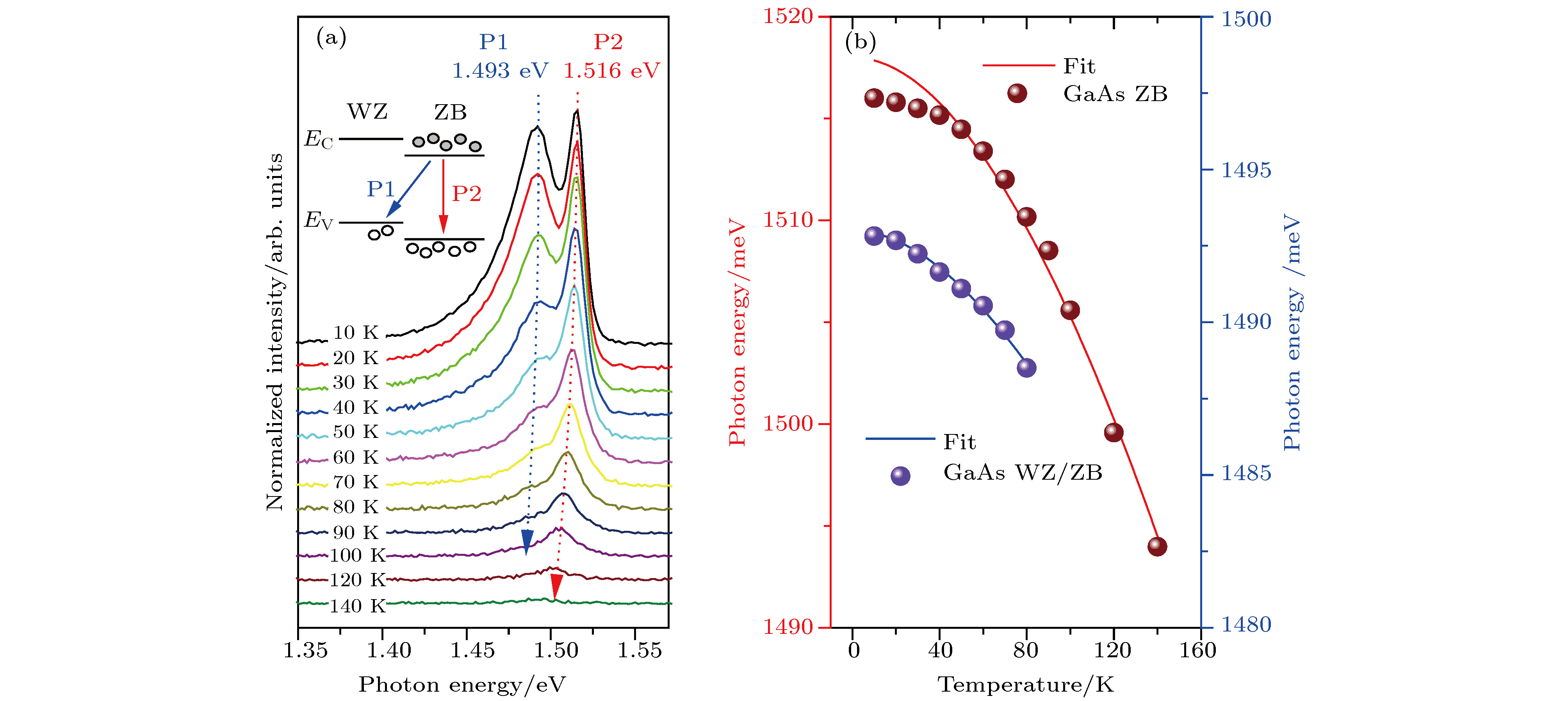
图 2 GaAs纳米线变温PL光谱测试图 (a)发光峰位随温度10−140 K的变化; (b) P1, P2发光峰峰位随温度变化的拟合曲线
Fig. 2. Variable power PL spectrum: (a) The change of luminescence peak position with temperature 10−140 K; (b) fitting curve of the peak position of P1 and P2 luminescence with the change of temperature
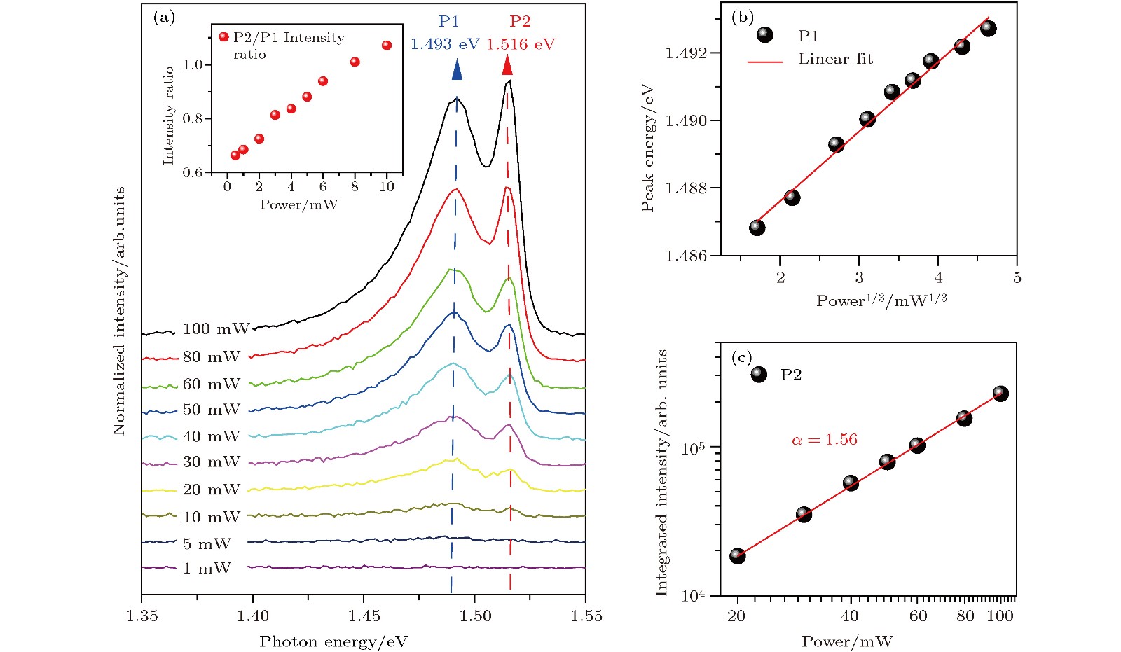
图 3 变功率PL光谱测试图 (a)不同功率下PL光谱曲线, 插图为P2, P1峰强比随功率变化曲线; (b) P1峰位与P1/3的关系; (c) P2峰强与功率的关系
Fig. 3. Variable power PL spectrum: (a) The PL spectral curve with different power is illustrated as the peak ratio of P2, P1 changing with power; (b) the relationship between P1 peak and P1/3; (c) the relationship between P2 peak intensity and power
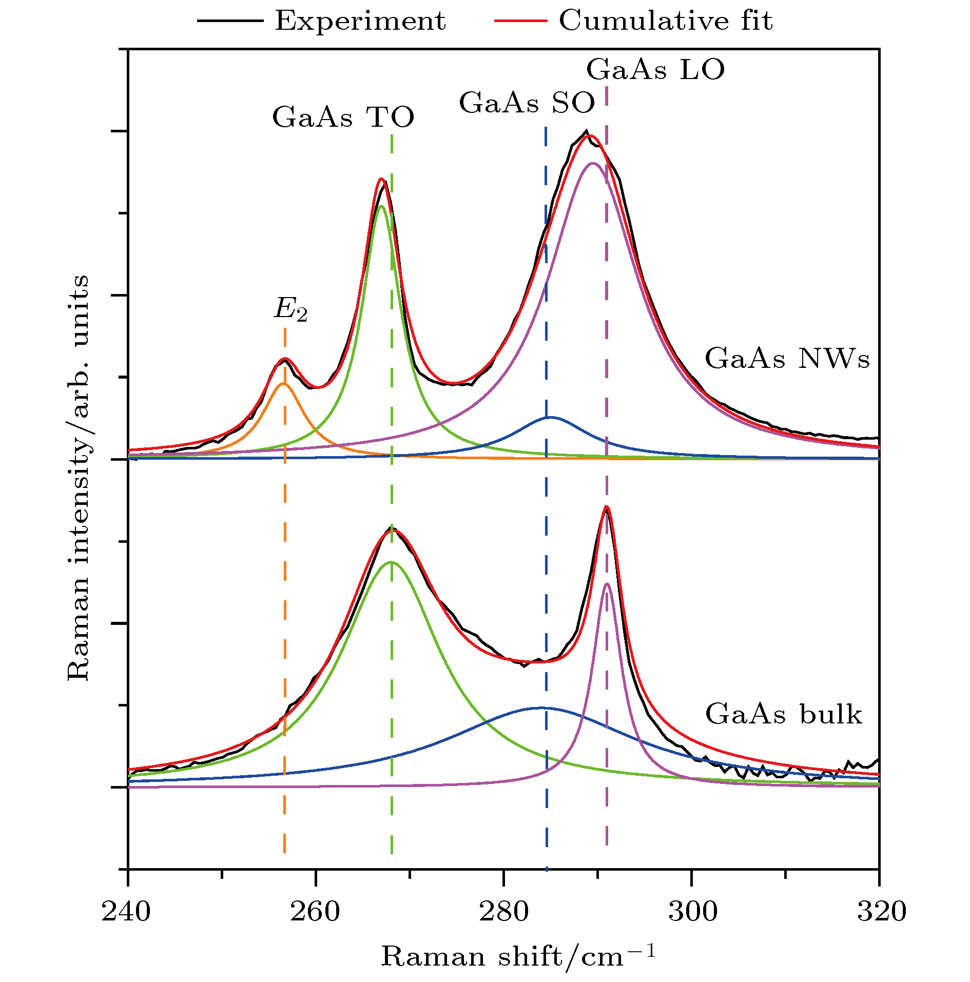
图 4 GaAs纳米线及GaAs衬底的Raman光谱图
Fig. 4. Raman spectra of GaAs nanowires and GaAs substrate
-
[1] Dai X, Zhang S, Wang Z L, Adamo G, Liu H, Huang Y Z, Couteau C, Soci C 2014 Nano Lett. 14 2688
Google Scholar
[2] Farrell A C, Senanayake P, Meng X, Hsieh N Y, Huffaker D L 2017 Nano Lett. 17 2420
Google Scholar
[3] Cammi D, Rodiek B, Zimmermann K, Kück S, Voss T 2017 J. Mater. Res. 32 2464
Google Scholar
[4] Tchernycheva M, Lavenus P, Zhang H, Babichev A V, Jacopin G, Shahmohammadi M, Julien F H, Ciechonski R, Vescovi G, Kryliouk O 2014 Nano Lett. 14 2456
Google Scholar
[5] Hussain L, Karimi M, Berg A, Jain V, Borgström M T, Gustafsson A, Samuelson L, Pettersson H 2017 Nanotechnology 28 485205
Google Scholar
[6] Ullah A R, Meyer F, Gluschke J G, Naureen S, Caroff P, Krogstrup P, Nygård J, Micolich A P 2018 Nano Lett. 18 5673
Google Scholar
[7] Price A, Martinez A 2015 J. Appl. Phys. 117 164501
Google Scholar
[8] Yang W, Pan D, Shen R, Wang X, Zhao J, Chen Q 2018 Nanotechnology 29 415230
[9] 毛宏伟, 刘一先, 李富铭 1990 中国激光 17 538
Google Scholar
Mao H W, Liu Y X, Li F M 1990 Chin. J. Las. 17 538
Google Scholar
[10] Han N, Wang F, Hou J J, Yip S, Lin H, Fang M, Xiu F, Shi X L, Hung T F, Ho J C 2012 Cryst. Growth Des. 12 6243
Google Scholar
[11] 夏宁, 方铉, 容天宇, 王登魁, 房丹, 唐吉龙, 王新伟, 王晓华, 李永峰, 姚斌, 魏志鹏 2018 中国激光 45 0603002
Xia N, Fang X, Rong T Y, Wang D K, Fang D, Tang J L, Wang X W, Wang X H, Li Y F, Yao B, Wei Z P 2018 Chin. J. Las. 45 0603002
[12] Glas F, Harmand J C, Patriarche G 2007 Phys. Rev. Lett. 99 146101
Google Scholar
[13] Hoang T B, Zhou H, Moses A F, Dheeraj D L, Helvoor A, Fimland B O, Weman H 2009 Mater. Res. Soc. Symp. Proc. 1144
[14] Vainorius N, Jacobsson D, Lehmann S, Gustafsson A, Dick K A, Samuelson L, Pistol M E 2014 Phys. Rev. B 89 165423
Google Scholar
[15] Kinzel J B, Schülein F J, Weiß M, Janker L, Bühler D D, Heigl M, Rudolph D, Morkötter S, Döblinger M, Bichler M, Abstreiter G, Finley J J, Wixforth A, Koblmüller G, Abstreiter G 2016 ACS Nano 10 4942
Google Scholar
[16] Senichev A, Corfdir P, Brandt O, Ramsteiner M, Breuer S, Schilling J, Geelhaar L, Werner P 2018 Nano Res. 1 14
[17] Mukherjee A, Ghosh S, Breuer S, Jahn U, Geelhaar L, Grahn H T 2017 J. Appl. Phys. 117 054308
[18] Kim H, Ren D, Farrell A C, Huffaker D L 2018 Nanotechnology 29 085601
Google Scholar
[19] 崔建功, 张霞, 颜鑫, 李军帅, 黄永清, 任晓敏 2014 物理学报 63 136103
Google Scholar
Cui J G, Zhang X, Yan X, Li J S, Huang Y Q, Ren X M 2014 Acta Phys. Sin. 63 136103
Google Scholar
[20] Liu Y, Peng Y, Guo J, La D, Xu Z 2018 AIP Adv. 8 055108
Google Scholar
[21] Zhou C, Zheng K, Liao Z M, Chen P P, Lu W, Zou J 2017 J. Mater. Chem. C 5 5257
Google Scholar
[22] Timofeeva M, Bouravleuv A, Cirlin G, Shtrom I, Soshnikov I, Reig Escalé M, Sergeyev A Grange R 2016 Nano Lett. 16 6290
Google Scholar
[23] Bussone G, Schäfer-Eberwein H, Dimakis E, Biermanns A, Carbone D, Tahraoui A, Geelhaar L, Bolívar P H, Schülli T U, Pietsch U 2015 Nano Lett. 15 981
Google Scholar
[24] Fontcuberta i Morral A, Colombo C, Abstreiter G, Arbiol J, Morante J R 2008 Appl. Phys. Lett. 92 063112
Google Scholar
[25] Bauer B, Rudolph A, Soda M, Fontcuberta i Morral A, Zweck J, Schuh D, Reiger E 2010 Nanotechnology 21 435601
Google Scholar
[26] Ramsteiner M, Brandt O, Kusch P, Breuer S, Reich S, Geelhaar L 2013 Appl. Phys. Lett. 103 043121
Google Scholar
[27] Jahn U, Lähnemann J, Pfüller C, Brandt O, Breuer S, Jenichen B, Ramsteiner M, Geelhaar L, Riechert H 2012 Phys. Rev. B 85 045323
Google Scholar
[28] Falcão B P, Leitão J P, Correia M R, Soares M R, Morales F M, Mánuel J M, Garcia R, Gustafsson A, Moreira M V B, de Oliveira A G, González J C 2013 J. Appl. Phys. 114 183508
Google Scholar
[29] Rudolph D, Schweickert L, Morkötter S, Loitsch B, Hertenberger S, Becker J, Bichler M, Abstreiter G, Finley J J, Koblmüller G 2013 Appl. Phys. Lett. 105 033111
[30] Varshni Y P 1967 Physica 34 149
Google Scholar
[31] Chiu Y S, Ya M H, Su W S, Chen Y F 2002 J. Appl. Phys. 92 5810
Google Scholar
[32] Jin S, Zheng Y, Li A 1997 J. Appl. Phys. 82 3870
Google Scholar
[33] Fang X, Wei Z P, Chen R, Tang J L, Zhao H F, Zhang L G, Zhao D X, Fang D, Li J H, Fang F, Chu X Y, Wang X H 2015 ACS Appl. Mater. Inter. 7 10331
Google Scholar
[34] Begum N, Piccin M, Jabeen F, Bais G, Rubini S, Martelli F, Bhatti A S 2008 J. Appl. Phys. 104 104311
Google Scholar
[35] Spirkoska D, Arbiol J, Gustafsson A, Conesa-Boj S, Glas F, Zardo I, Heigoldt M, Gass M H, Bleloch A L, Estrade S, Kaniber M, Rossler J, Peiro F, Morante J R, Abstreiter G, Samuelson L, Fontcuberta i Morral A 2009 Phys. Rev. B 80 245325
Google Scholar

 下载:
下载:
计量
- 文章访问数: 16176
- PDF下载量: 196
- 被引次数: 0
