


-
近年来, 宽带隙半导体材料氧化镓在日盲紫外探测领域的应用引起了广泛关注. 本文基于溶液法制备了非晶氧化镓薄膜, 采用紫外光退火的方式降低了薄膜的制备温度, 并且通过铝颗粒修饰氧化镓薄膜表面, 提升了氧化镓紫外探测器的性能. 紫外退火的方式可将氧化镓薄膜的制备温度降至300 ℃, 有望实现柔性器件的制备. 当沉积铝膜厚度在3—5 nm时, 可获得分布均匀、直径为2—3 nm的铝颗粒, 经修饰的氧化镓薄膜表现出优秀的光电响应性能和日盲探测特性. 在254 nm光照下, 最大光暗电流比可达2.55×10⁴, 在紫外波段的抑制比I254 nm/I365 nm为2.2×10⁴. 最佳的探测器响应度和探测率分别为0.771 A/W和1.13×1011 Jones, 相比于未做修饰的氧化镓紫外探测器提升了约34倍和36倍. 然而, 铝纳米颗粒的修饰也会引入部分缺陷态, 导致氧化镓光电探测器响应下降时间的增大.Gallium oxide (Ga2O3) as a wide bandgap semiconductor material has attracted much attention in the field of solar blind ultraviolet photodetection recently. Localized surface plasmon resonance is considered an effective way to improve the performance of optoelectronic devices by decorating the materials with metal particles. Al nanoparticle is a potential candidate for ultraviolet photodetectors because its suitable resonance wavelength is located in the ultraviolet wavelength range. In this work, the preparation temperature of the Ga2O3 thin film is reduced by ultraviolet photo-annealing, and the amorphous Ga2O3 thin film is prepared by using the solution method. In addition, aluminum (Al) nanoparticles are used to decorate the surface of Ga2O3 thin film through thermal evaporation of aluminum film and then annealing, which improves the optoelectrical performance in the solar-blind wavelength spectrum. The X-ray diffraction (XRD) is employed to demonstrate the amorphous Ga2O3 thin film. The surface roughness and the diameters of Al nanoparticles are analyzed by atomic force microscope (AFM). When the thickness of the deposited Al layer is about 3–5 nm, Al particles with the diameters in a range of 2–3 nm can be obtained. When the thickness of the deposited Al layer is more than 7 nm, Al nanoparticles turn into the particles with non-identical diameters and distribute in the form of agglomeration. Transmittance spectrum and absorption spectrum are employed to characterize the optical properties. The bandgaps of different samples are obtained, and the results are consistent with the theoretical ones. The Ga2O3 thin film shows excellent optoelectrical performance and solar blind rejection ratio. Under 254 nm illumination, the maximum photo-to-dark current ratio is 2.55×10⁴, and the rejection ratio of I254 nm/I365 nm is 2.2×10⁴. The best responsivity and detectivity of prepared samples are 0.771 A/W and 1.13×10¹¹ Jones, which are about 34 times and 36 times higher than those without Al decoration. The improvement is attributed to the scattering effect of surface Al nanoparticles for illumination, which enhances the Ga2O3 thin film absorption of solar blind ultraviolet light. Meanwhile, owing to the localized surface plasma resonance, the local electromagnetic fields generated near the Al nanoparticles promote the transfer of carriers in the film. Furthermore, the point about how the Al nanoparticles decorated on the surface of Ga2O3 thin film influence the time response is also discussed in this work. As a result, the introduction of defect states will lead to an increase of fall time due to the Al deposition. In this work, the effect of Al nanoparticles decoration on the optoelectrical performance of amorphous Ga2O3 thin film solar blind ultraviolet photodetectors is studied based on a simple preparation, which provides a possible pathway for developing the flexible solar blind electronic devices in the future.
-
Keywords:
- gallium oxide /
- solar blind ultraviolet photodetector /
- solution method /
- Al nanoparticles
[1] Chen H, Liu K, Hu L, Al-Ghamdi A A, Fang X 2015 Mater. Today 18 493
 Google Scholar
[2] Razeghi M 2002 Proc. IEEE 90 1006
Google Scholar
[3] Sang L, Liao M, Sumiya M 2013 Sensors (Basel) 13 10482
Google Scholar
[4] Liao M, Wang X, Teraji T, Koizumi S, Koide Y 2010 Phys. Rev. B 81 033304
Google Scholar
[5] Cicek E, McClintock R, Cho C Y, Rahnema B, Razeghi M 2013 Appl. Phys. Lett. 103 051102
Google Scholar
[6] Suzuki R, Nakagomi S, Kokubun Y, Arai N, Ohira S 2009 Appl. Phys. Lett. 94 222102
Google Scholar
[7] Yang J L, Liu K W, Shen D Z 2017 Chin. Phys. B 26 047308
Google Scholar
[8] Wu Z H, Qian L X, Sheng T, Zhang Y Y, Liu X Z 2019 IEEE International Conference on Electron Devices & Solid-state Circuits Xi'an China, June 12–14, 2019 p82
[9] Chang K W, Wu J J 2005 Adv. Mater. 17 241
Google Scholar
[10] Guo D Y, Wu Z P, Li P G, An Y H, Liu H, Guo X C, Yan H, Wang G F, Sun C L, Li L H, Tang W H 2014 Opt. Mater. Express 4 1067
Google Scholar
[11] Yu F P, Ou S L, Wuu D S 2015 Opt. Mater. Express 5 1240
Google Scholar
[12] He H Y, Orlando R, Blanco M A, Pandey R, Amzallag E, Baraille I, Rérat M 2006 Phys. Rev. B 74 195123
Google Scholar
[13] Gottschalch V, Merker S, Blaurock S, Kneiß M, Teschner U, Grundmann M, Krautscheid H 2019 J. Cryst. Growth 510 76
Google Scholar
[14] Pearton S J, Yang J C, Cary P H, Ren F, Kim J, Tadjer M J, Mastro M A 2018 Appl. Phys. Rev. 5 011301
Google Scholar
[15] Dong L P, Yu J G, Jia R X, Hu J C, Zhang Y M, Sun J W 2019 Opt. Mater. Express 9 1191
Google Scholar
[16] Qian L X, Wang Y, Wu Z H, Sheng T, Liu X Z 2017 Vacuum 140 106
Google Scholar
[17] Liu X Z, Guo P, Sheng T, Qian L X, Zhang W L, Li Y R 2016 Opt. Mater. 51 203
Google Scholar
[18] Alema F, Hertog B, Ledyaev O, Volovik D, Thoma G, Miller R, Osinsky A, Mukhopadhyay P, Bakhshi S, Ali H, Schoenfeld W V 2017 Phys. Status Solidi A 214 1600688
Google Scholar
[19] Wang H, Chen H, Li L, Wang Y, Su L, Bian W, Li B, Fang X 2019 J. Phys. Chem. Lett. 10 6850
Google Scholar
[20] Mayer K M, Hafner J H 2011 Chem. Rev. 111 3828
Google Scholar
[21] Zhang Y, Lin N, Li Y, Wang X, Wang H, Kang J, Wilks R, Bar M, Mu R 2016 Sci. Rep. 6 23106
Google Scholar
[22] 刘伦涛 2020 博士学位论文 (济南: 山东大学)
Liu L T 2020 Ph. D. Dissertation (Jinan: Shandong University) (in Chinese)
[23] An Y, Chu X, Huang Y, Zhi Y, Guo D, Li P, Wu Z, Tang W 2016 Prog. Nat. Sci. 26 65
Google Scholar
[24] Shi X, Yang Z, Yin S, Zeng H 2016 Mater. Technol. 31 544
Google Scholar
[25] Chang Y T, Chuang T H, Tsai M W, Chen L C, Lee S C 2007 J. Appl. Phys. 101 054305
Google Scholar
[26] Rafique S, Han L, Zhao H 2016 Phys. Status Solidi A 213 1002
Google Scholar
[27] Cui S, Mei Z, Hou Y, Sun M, Chen Q, Liang H, Zhang Y, Bai X, Du X 2018 Sci Chin.-Phys. Mech. Astron. 61 107021
Google Scholar
[28] Zhao B, Wang F, Chen H Y, Zheng L X, Su L X, Zhao D X, Fang X S 2017 Adv. Funct. Mater. 27 1700264
Google Scholar
[29] Guo D Y, Su Y L, Shi H Z, Li P G, Zhao N, Ye J H, Wang S L, Liu A P, Chen Z W, Li C R, Tang W H 2018 ACS Nano 12 12827
Google Scholar
[30] Zhang D, Zheng W, Lin R C, Li T T, Zhang Z J, Huang F 2018 J. Alloys Compd. 735 150
Google Scholar
-
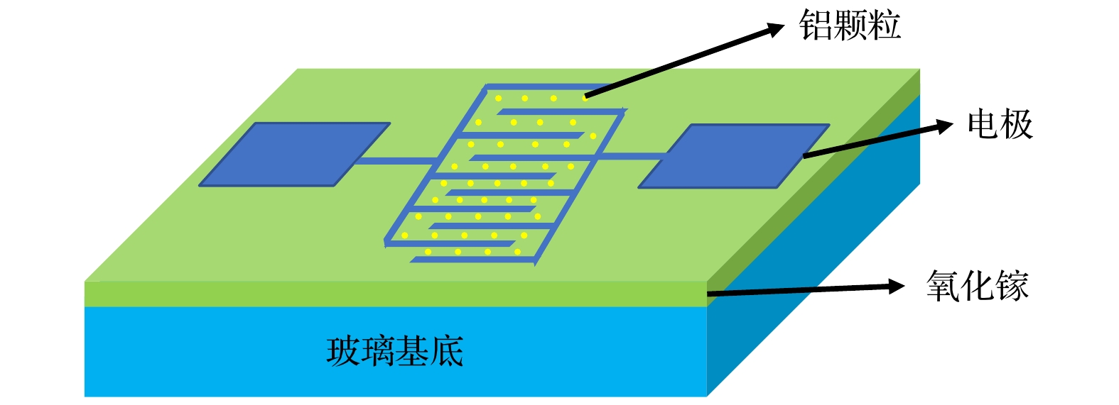
图 1 铝纳米颗粒修饰非晶Ga2O3探测器结构示意图
Fig. 1. Schematic device structure of the Al nanoparticles decorated amorphous Ga2O3 thin film photodetector.
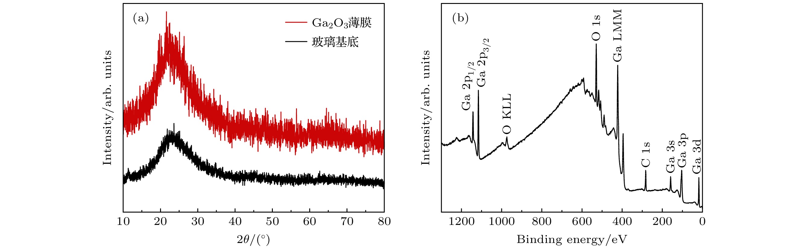
图 2 (a) Ga2O3薄膜XRD图谱; (b) Ga2O3薄膜XPS能谱
Fig. 2. (a) XRD patterns of Ga2O3 thin film; (b) XPS spectrum of Ga2O3 thin film.
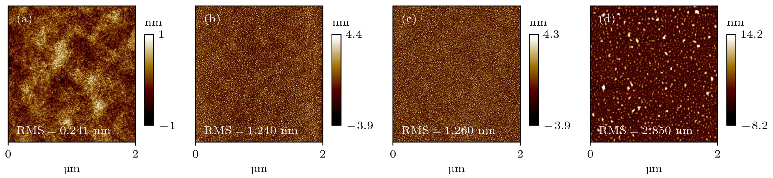
图 3 Ga2O3薄膜表面AFM图 (a) 未沉积铝颗粒; (b) 沉积3 nm铝; (c) 沉积5 nm铝; (d) 沉积7 nm铝
Fig. 3. The AFM images of Ga2O3: (a) Without Al Nanoparticles; (b) with 3 nm Al layer; (c) with 5 nm Al layer; (d) with 7 nm Al layer.
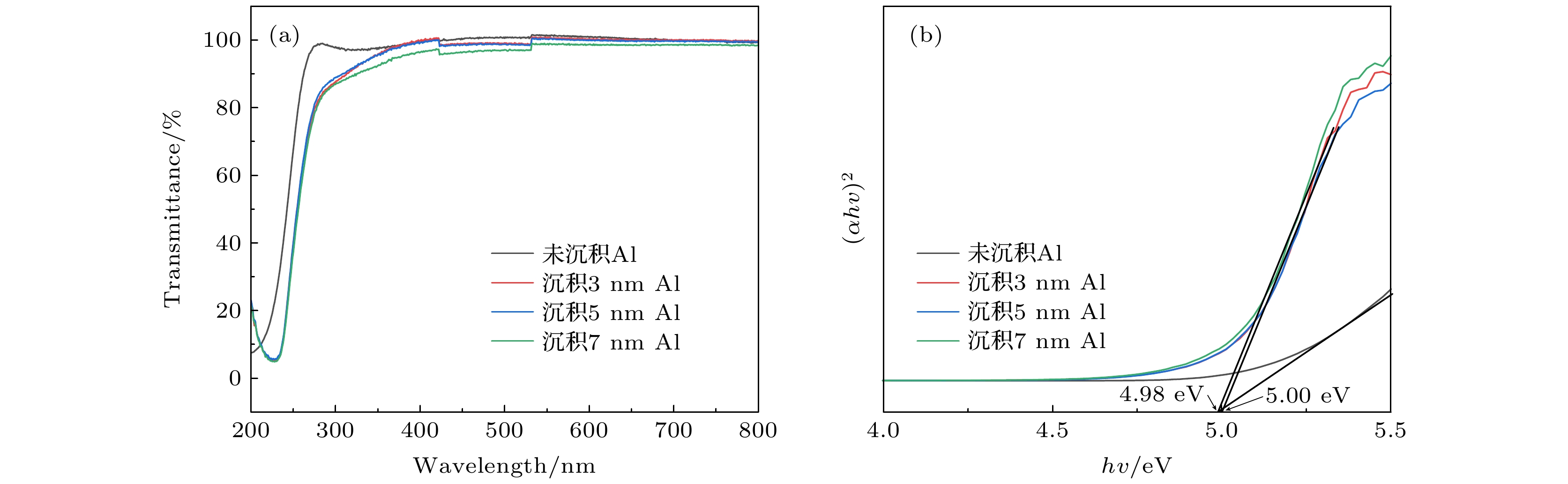
图 4 (a) 不同铝厚度下Ga2O3薄膜透过率曲线以及(b) (αhv)2-hv 曲线
Fig. 4. (a) Transmittance spectra and (b) curves of (αhv)2-hv of Ga2O3 thin film with different Al thickness.

图 5 未沉积铝和沉积不同厚度铝Ga2O3紫外探测器的I-V特性曲线 (a) 暗电流; (b) 254 nm光照下的光电流; (c) 365 nm光照下的光电流
Fig. 5. Electrical performance of Ga2O3 photodetectors with/without Al decoration: (a) Dark current; (b) photocurrent under 254 nm illumination; (c) photocurrent under 365 nm illumination.
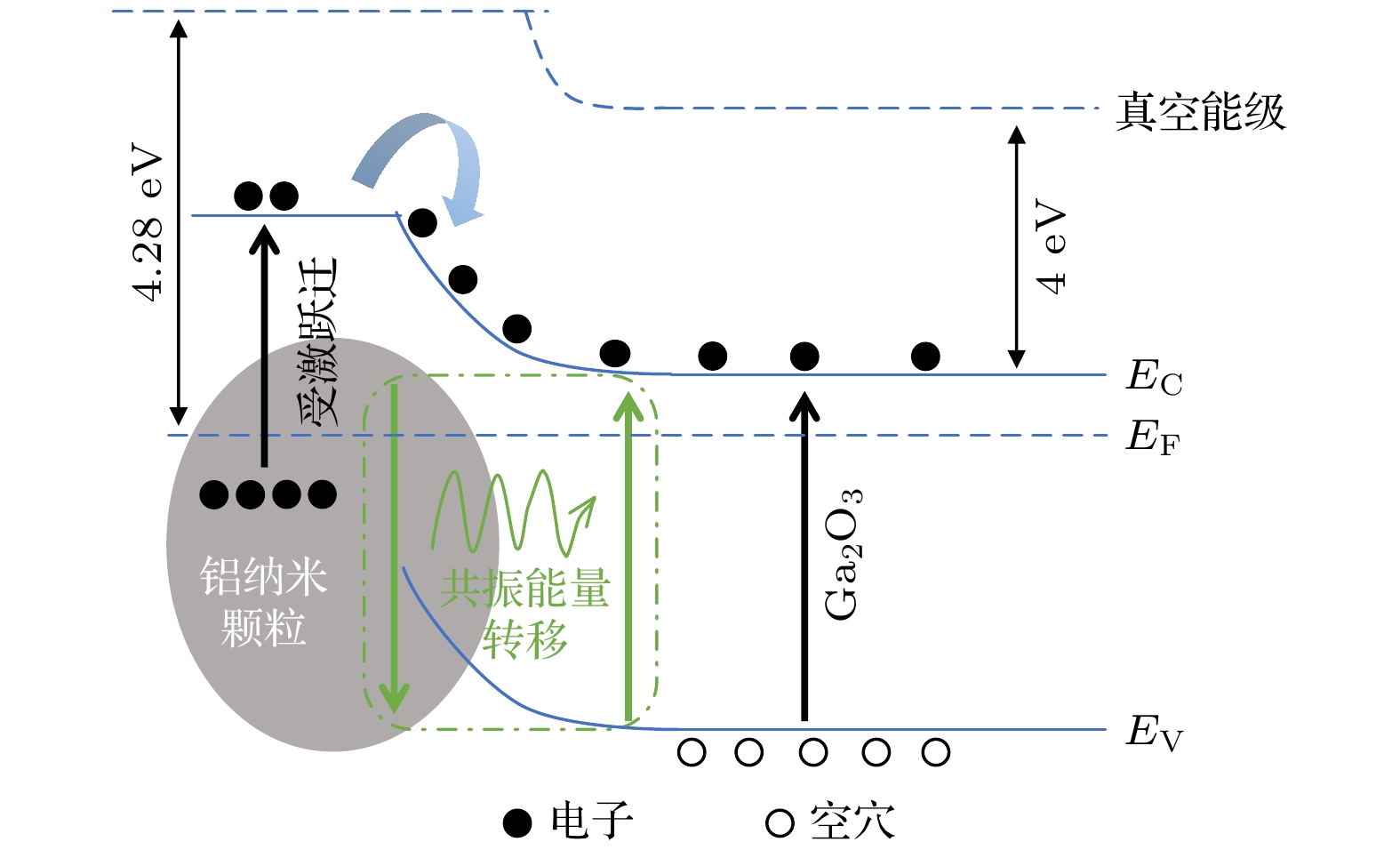
图 6 铝纳米颗粒/Ga2O3薄膜界面处的能带与电子转移机制
Fig. 6. Schematic illustration of the energy band and electron transfer mechanisms at Al nanoparticles/Ga2O3 interface.
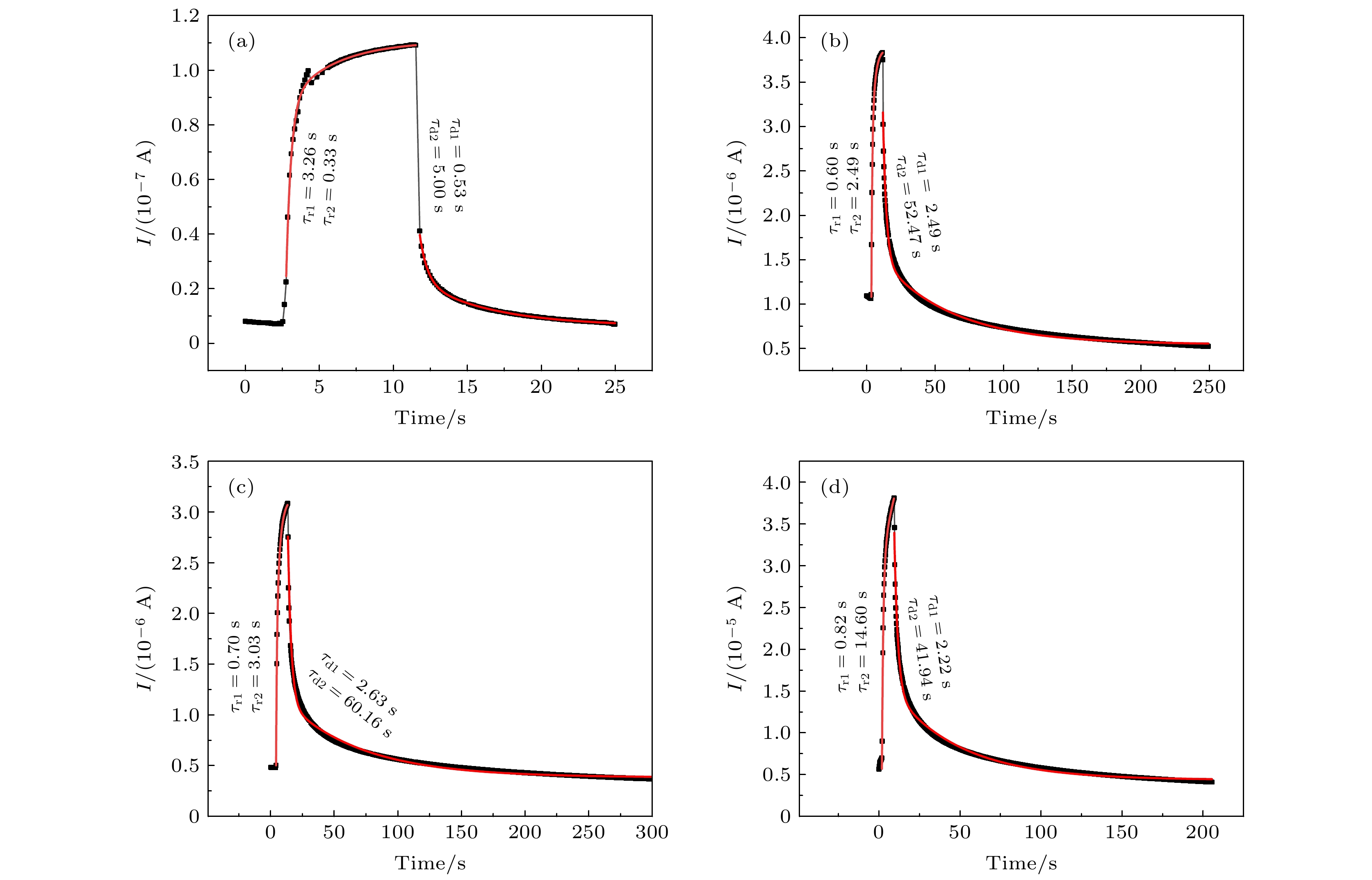
图 7 Ga2O3紫外探测器的时间响应曲线 (a) 未沉积铝; (b) 沉积3 nm铝; (c) 沉积5 nm铝; (d) 沉积7 nm铝
Fig. 7. Time response curves of Ga2O3 photodetectors: (a) Without Al; (b) with 3 nm Al layer; (c) with 5 nm Al layer; (d) with 7 nm Al layer.
表 1 20 V偏压下沉积3 nm /5 nm /7 nm以及未沉积样品的电学参数
Table 1. Electrical parameters of samples with 3 nm /5 nm /7 nm Al and without Al under 20 V bias.
铝层
厚度/nmIdark/A I254 nm/A I365 nm/A I254 nm/Idark I254 nm/I365 nm R254 nm/
(A·W–1)R365 nm/
(A·W–1)R254 nm/R365 nm $D_{\rm 254\;nm}^*$/Jones 未沉积 1.51×10⁻¹⁰ 1.15×10⁻⁷ 1.74×10⁻¹⁰ 7.62×10² 6.61×10² 0.0228 4.56×10⁻⁶ 4993 3.13×10⁹ 3 1.52×10⁻¹⁰ 3.88×10⁻⁶ 1.79×10⁻¹⁰ 2.55×10⁴ 2.17×10⁴ 0.771 5.36×10⁻⁶ 1.44×10⁵ 1.13×10¹¹ 5 1.34×10⁻¹⁰ 3.32×10⁻⁶ 1.51×10⁻¹⁰ 2.48×10⁴ 2.20×10⁴ 0.659 3.37×10⁻⁶ 1.95×10⁵ 1.03×10¹¹ 7 3.33×10⁻¹⁰ 6.88×10⁻⁵ 4.46×10⁻⁷ 2.07×10⁵ 1.54×10² 13.647 0.0884 154 1.35×10¹²  下载: 导出CSV
-
[1] Chen H, Liu K, Hu L, Al-Ghamdi A A, Fang X 2015 Mater. Today 18 493
Google Scholar
[2] Razeghi M 2002 Proc. IEEE 90 1006
Google Scholar
[3] Sang L, Liao M, Sumiya M 2013 Sensors (Basel) 13 10482
Google Scholar
[4] Liao M, Wang X, Teraji T, Koizumi S, Koide Y 2010 Phys. Rev. B 81 033304
Google Scholar
[5] Cicek E, McClintock R, Cho C Y, Rahnema B, Razeghi M 2013 Appl. Phys. Lett. 103 051102
Google Scholar
[6] Suzuki R, Nakagomi S, Kokubun Y, Arai N, Ohira S 2009 Appl. Phys. Lett. 94 222102
Google Scholar
[7] Yang J L, Liu K W, Shen D Z 2017 Chin. Phys. B 26 047308
Google Scholar
[8] Wu Z H, Qian L X, Sheng T, Zhang Y Y, Liu X Z 2019 IEEE International Conference on Electron Devices & Solid-state Circuits Xi'an China, June 12–14, 2019 p82
[9] Chang K W, Wu J J 2005 Adv. Mater. 17 241
Google Scholar
[10] Guo D Y, Wu Z P, Li P G, An Y H, Liu H, Guo X C, Yan H, Wang G F, Sun C L, Li L H, Tang W H 2014 Opt. Mater. Express 4 1067
Google Scholar
[11] Yu F P, Ou S L, Wuu D S 2015 Opt. Mater. Express 5 1240
Google Scholar
[12] He H Y, Orlando R, Blanco M A, Pandey R, Amzallag E, Baraille I, Rérat M 2006 Phys. Rev. B 74 195123
Google Scholar
[13] Gottschalch V, Merker S, Blaurock S, Kneiß M, Teschner U, Grundmann M, Krautscheid H 2019 J. Cryst. Growth 510 76
Google Scholar
[14] Pearton S J, Yang J C, Cary P H, Ren F, Kim J, Tadjer M J, Mastro M A 2018 Appl. Phys. Rev. 5 011301
Google Scholar
[15] Dong L P, Yu J G, Jia R X, Hu J C, Zhang Y M, Sun J W 2019 Opt. Mater. Express 9 1191
Google Scholar
[16] Qian L X, Wang Y, Wu Z H, Sheng T, Liu X Z 2017 Vacuum 140 106
Google Scholar
[17] Liu X Z, Guo P, Sheng T, Qian L X, Zhang W L, Li Y R 2016 Opt. Mater. 51 203
Google Scholar
[18] Alema F, Hertog B, Ledyaev O, Volovik D, Thoma G, Miller R, Osinsky A, Mukhopadhyay P, Bakhshi S, Ali H, Schoenfeld W V 2017 Phys. Status Solidi A 214 1600688
Google Scholar
[19] Wang H, Chen H, Li L, Wang Y, Su L, Bian W, Li B, Fang X 2019 J. Phys. Chem. Lett. 10 6850
Google Scholar
[20] Mayer K M, Hafner J H 2011 Chem. Rev. 111 3828
Google Scholar
[21] Zhang Y, Lin N, Li Y, Wang X, Wang H, Kang J, Wilks R, Bar M, Mu R 2016 Sci. Rep. 6 23106
Google Scholar
[22] 刘伦涛 2020 博士学位论文 (济南: 山东大学)
Liu L T 2020 Ph. D. Dissertation (Jinan: Shandong University) (in Chinese)
[23] An Y, Chu X, Huang Y, Zhi Y, Guo D, Li P, Wu Z, Tang W 2016 Prog. Nat. Sci. 26 65
Google Scholar
[24] Shi X, Yang Z, Yin S, Zeng H 2016 Mater. Technol. 31 544
Google Scholar
[25] Chang Y T, Chuang T H, Tsai M W, Chen L C, Lee S C 2007 J. Appl. Phys. 101 054305
Google Scholar
[26] Rafique S, Han L, Zhao H 2016 Phys. Status Solidi A 213 1002
Google Scholar
[27] Cui S, Mei Z, Hou Y, Sun M, Chen Q, Liang H, Zhang Y, Bai X, Du X 2018 Sci Chin.-Phys. Mech. Astron. 61 107021
Google Scholar
[28] Zhao B, Wang F, Chen H Y, Zheng L X, Su L X, Zhao D X, Fang X S 2017 Adv. Funct. Mater. 27 1700264
Google Scholar
[29] Guo D Y, Su Y L, Shi H Z, Li P G, Zhao N, Ye J H, Wang S L, Liu A P, Chen Z W, Li C R, Tang W H 2018 ACS Nano 12 12827
Google Scholar
[30] Zhang D, Zheng W, Lin R C, Li T T, Zhang Z J, Huang F 2018 J. Alloys Compd. 735 150
Google Scholar

 下载:
下载:
计量
- 文章访问数: 5333
- PDF下载量: 137
- 被引次数: 0
