


-
热电堆红外探测器主要是由热电偶为基本单元所构成的一种探测器件, 因其原理简单、工作时不需要冷却设备等优势已被广泛应用在生产生活的各个方面. 然而, 传统热电堆器件所选用材料的吸收率通常处在较低水平, 并且大部分与微加工工艺不兼容. 在此, 本文设计提出了一种带有垂直石墨烯(vertical graphene, VG)的金属热电堆红外探测器. 通过等离子体增强化学气相沉积(plasma enhanced chemical vapor deposition, PECVD)生长VG并将其保留在器件的热结处, 从而实现热电堆红外探测器的宽带和高响应特性. 这种复合结构的探测器在波长792 nm的情况下, 室温响应率最高可达1.53 V/W, 与没有VG的热电堆红外探测器相比, 前后响应结果可增加28倍左右, 响应时间缩短至0.8 ms左右. 该制备过程与微加工工艺相兼容, 同时整体提升了器件性能, 并适合于大规模生产. 此外, 利用表面等离激元共振的原理将VG与金属纳米颗粒相互结合, 发现在前后同等条件下材料的光吸收有明显的增强, 所产生的热电势响应最高可增6倍. 以上结果表明, VG在多种应用中具有巨大的潜力, 包括光电检测、微发电装置等, 该技术为制备高性能热电堆红外探测器和其他传感器件提供了一种新的途径.Thermopile infrared detector is a kind of detector device mainly composed of thermocouple as the basic unit. Because of its simple principle, no need of cooling equipment, and other advantages, it has been widely used in various fields of production and life. However, the absorption rates of the materials in conventional thermopile devices are poor, and the majority of them are incompatible with microfabrication methods. In this work, a metal thermopile infrared detector with vertical graphene (VG) is designed and fabricated. The VG is grown via plasma enhanced chemical vapor deposition, and retained at the device’s thermal ends to provide the thermopile IR detector’s wideband and high response characteristics. The detector achieves a room temperature responsivity reaching a value as high as 1.53 V/W at 792 nm, which can increase the response results about 28 times and reduce the response time to 0.8 ms compared with the thermopile detector without VG. After systematically measuring the response results, it is finally found that there are three main mechanisms responsible for the response on the composite device. The first one is the response generated by the metal thermopile itself alone. The second one is the response increased eventually by the contribution of VG covered at the metal thermal junction that expands the temperature difference. The last one is the response generated by the temperature gradient existing inside the VG on the surface of the device after the absorption of heat. The portion of each partial response mechanism in the total response is also analyzed, providing a new reference direction for analyzing the response generation mechanism of thermopile detectors with other absorbing materials. The process is compatible with the microfabrication, while the device performance is enhanced and suitable for mass production. Furthermore, by utilizing the surface plasmon resonance to combine VG with metal nanoparticles, the material’s light absorption is found to be enhanced significantly under the same conditions, and the resulting thermal voltage can be increased to 6 times. The results indicate that VG promises to possess practical applications, in many fields such as photoelectric sensing and power production devices. This technology provides a new method to manufacture high-performance thermopile infrared detectors and other sensor devices.
-
Keywords:
- vertical graphene /
- thermopiles /
- infrared detectors /
- surface plasmon resonance
[1] Xia F, Mueller T, Lin Y, Valdes-Garcia A, Avouris P 2009 Nat. Nanotechnol. 4 839
 Google Scholar
[2] Mittendorff M, Winnerl S, Kamann J, Eroms J, Weiss D, Schneider H, Helm M 2013 Appl. Phys. Lett. 103 021113
Google Scholar
[3] Compton O C, Nguyen S B T 2010 Small 6 711
Google Scholar
[4] Katsnelson M I 2007 Mater. Today 10 20
[5] Nair R R, Blake P, Grigorenko A N, Novoselov K S, Booth T J, Stauber T, Peres N M R, Geim A K 2008 Science 320 1308
Google Scholar
[6] Liu C, Chang Y, Norris T B, Zhong Z 2014 Nat. Nanotechnol. 9 273
Google Scholar
[7] Shi S F, Xu X, Ralph D C, McEuen P L 2011 Nano Lett. 11 1814
Google Scholar
[8] Emani N K, Chung T F, Ni X, Kildishev A V, Chen Y P, Boltasseva A 2012 Nano Lett. 12 5202
Google Scholar
[9] Lee H, Heo K, Park J, Park Y, Noh S, Kim K S, Lee C, Hong B H, Jian J, Hong S 2012 J. Mater. Chem. 22 8372
Google Scholar
[10] Babichev A V, Zhang H, Lavenus P, Julien F H, Egorov A Y, Lin Y T, Tu L W, Tchernycheva M 2013 Appl. Phys. Lett. 103 201103
Google Scholar
[11] Konstantatos G, Badioli M, Gaudreau L, Osmond J, Bernechea M, De Arquer P G F, Gatti F, Koppens F H 2012 Nat. Nanotechnol. 7 363
Google Scholar
[12] Bo Z, Yang Y, Chen J, Yu K, Yan J, Cen K 2013 Nanoscale 5 5180
Google Scholar
[13] Bo Z, Mao S, Han Z J, Cen K, Chen J, Ostrikov K K 2015 Chem. Soc. Rev. 44 2108
Google Scholar
[14] Zhu W, Xue Z Y, Wang G, Zhao M H, Chen D, Guo Q L, Liu Z D, Feng X Q, Ding G Q, Chu P K, Di Z F 2020 ACS Appl. Nano Mater. 3 6915
Google Scholar
[15] Yu K, Wang P, Lu G, Chen K H, Bo Z, Chen J 2011 J. Phys. Chem. Lett. 2 537
Google Scholar
[16] Graf A, Arndt M, Sauer M, Gerlach G 2007 Meas. Sci. Technol. 18 R59
Google Scholar
[17] Chaglla E J S, Celik N, Balachandran W 2018 Sensors 18 3315
Google Scholar
[18] Moisello E, Malcovati P, Bonizzoni E 2021 Micromachines 12 148
Google Scholar
[19] Buchner R, Sosna C, Maiwald M, Benecke W, Lang W 2006 Sens. Actuators, A 130 262
[20] Dijkstra M, Lammerink T S, de Boer M J, Berenschot E J W, Wiegerink R J, Elwenspoek M 2014 J. Microelectromech. Syst. 23 908
Google Scholar
[21] Randjelovic D, Petropoulos A, Kaltsas G, Stojanovic M, Lazic Z, Djuric Z, Matic M 2008 Sens. Actuators, A 141 404
Google Scholar
[22] Yoo K P, Hong H P, Lee M J, Min S J, Park C W, Choi W S, Min N K 2011 Meas. Sci. Technol. 22 115206
Google Scholar
[23] Itoigawa K, Ueno H, Shiozaki M, Toriyama T, Sugiyama S 2005 J. Micromech. Microeng. 15 S233
Google Scholar
[24] Dhawan R, Madusanka P, Hu G Y, Debord J, Tran T, Maggio K, Edwards H, Lee M 2020 Nat. Commun. 11 4362
Google Scholar
[25] Xu D H, Wang Y L, Xiong B, Li T 2017 Front. Mech. Eng. 12 557
Google Scholar
[26] Shahmarvandi E K, Ghaderi M, Wolffenbuttel R F 2016 J. Phys. Conf. Ser. 757 012033
Google Scholar
[27] Xu D, Xiong B, Wang Y 2010 IEEE Electron Device Lett. 31 512
Google Scholar
[28] Zhang C C, Mao H Y, Shi M, Xiong J J, Long K W, Chen D P 2020 33rd IEEE International Confence on Micro Electro Mechannical Systems (MEMS 2020) Vancouver, Canada, January 18–22, 2020 p949
[29] Qian F, Deng J, Xiong F, Dong Y, Xu C 2020 Opt. Mater. Express 10 2909
Google Scholar
[30] Li X, Zhu M, Du M, Lv Z, Zhang L, Li Y, Yang Y, Yang T, Li X, Wang K, Zhu Y, Fang Y 2016 Small 12 549
Google Scholar
[31] Tian W, Wang Y, Zhou H, Wang Y L, Li T 2020 J. Microelectromech Syst. 29 36
Google Scholar
[32] Sofiane B M, Sébastien E, Thomas B, Laurent T, Pascal V, Danick B, Jean-Paul G, Laurent C 2015 Microsyst. Technol. 21 1627
Google Scholar
[33] Allen L H, Patrick K H, Nathaniel M G, Sungjae H, Yong C S, Yi S, Matthew C, Madan D, Anantha P C, Jing K, Pablo J, Tomás P 2015 Nano Lett. 15 7211
Google Scholar
[34] Willets K A, Van Duyne, R P 2007 Ann. Rev. Phys. Chem. 58 267
Google Scholar
-

图 1 PECVD系统反应腔室结构示意图
Fig. 1. Schematic diagram of the structure of the reaction chamber of the PECVD system.

图 2 (a)—(e) VG热电堆探测器制备流程; (f) VG热电堆探测器及器件测试示意图
Fig. 2. (a)–(e) Preparation process of VG thermopile detector; (f) schematic diagram of the VG thermopile detector and device measuring.
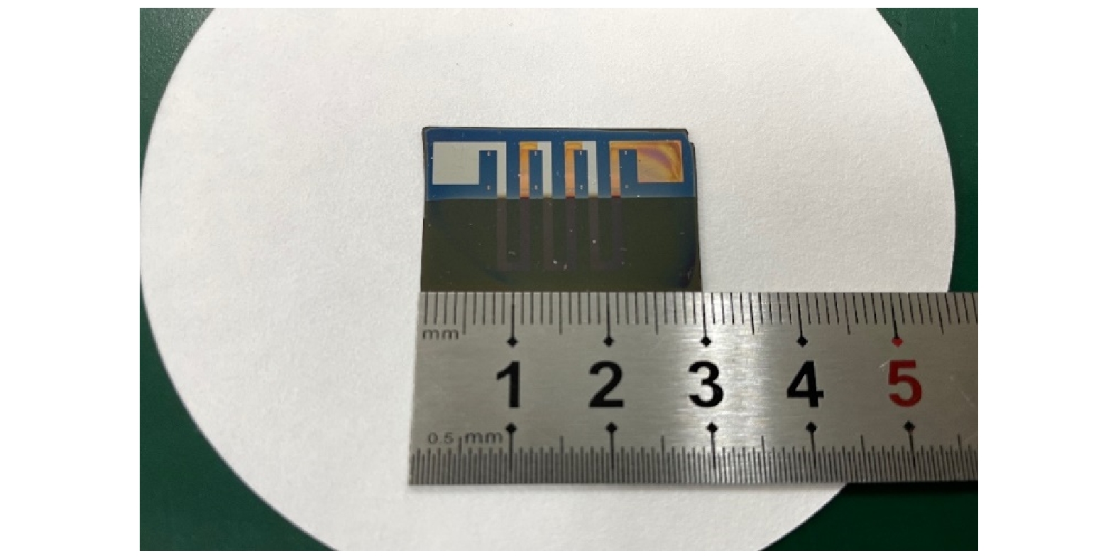
图 3 带有VG金属热电堆红外探测器实物图
Fig. 3. Physical image of infrared detector with VG metal thermopile.
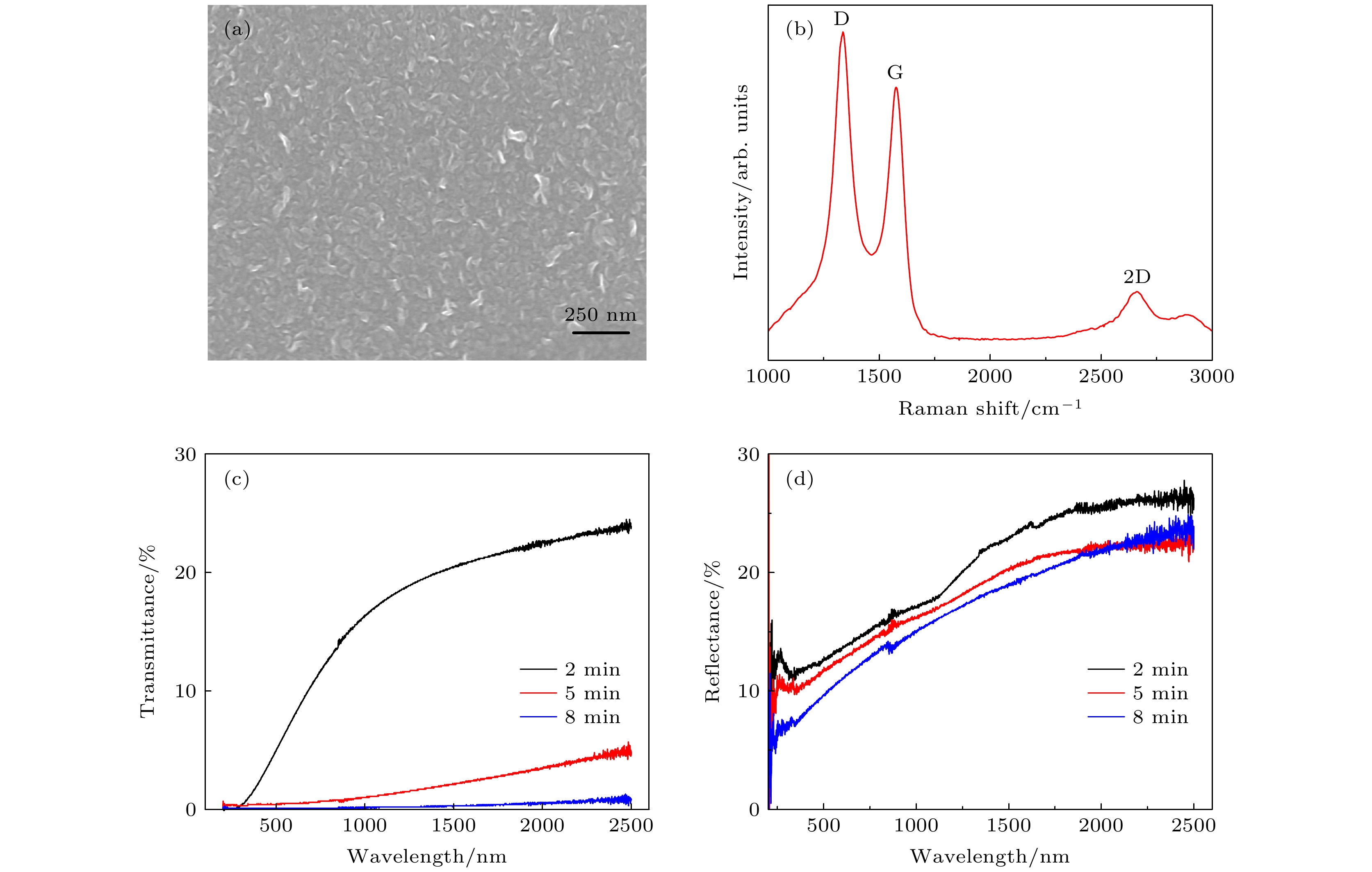
图 4 VG的(a) SEM图和(b)拉曼光谱图; 不同生长时间的VG对应的(c)光透射率和(d)反射率
Fig. 4. (a) SEM image and (b) Raman spectrum of VG; (c), (d) corresponding optical transmittance (c) and reflectance (d) of VG with different growth time.

图 5 器件在(a), (b) 792和(c), (d) 1550 nm下的响应结果 (a), (c) 仅有金属的热电堆器件; (b), (d) 带有VG的金属热电堆器件
Fig. 5. Response results of the device at (a), (b) 792 and (c), (d) 1550 nm: (a), (c) Metal-only thermopile device; (b), (d) metal thermopile device combined with VG.

图 6 VG热电堆探测器在792 nm下的测试结果 (a) 响应测试示意图; (b) 仅有金属的器件光照在左端; (c) 仅有金属的器件光照在右端; (d) 带有VG的器件光照在左端; (e) 带有VG的器件光照在中点; (f) 带有VG的器件光照在右端
Fig. 6. Measure results of VG thermopile detector at 792 nm: (a) Measure schematic diagram; (b) metal-only device (laser on the left end); (c) metal-only device (laser on the right end); (d) with VG device (laser on the left end); (e) with VG device (laser on the midpoint); (f) with VG device (laser on the right end).
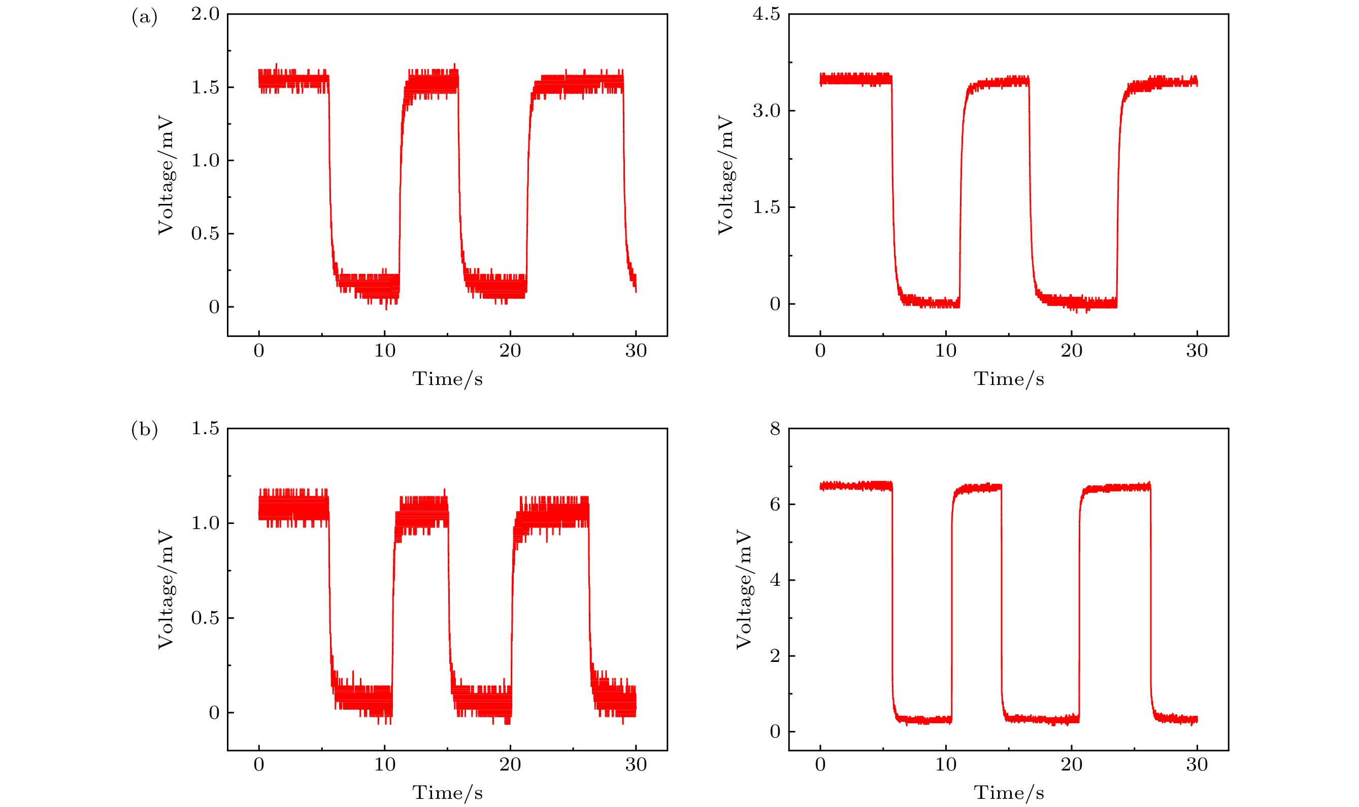
图 10 VG与金属纳米颗粒结合前后的响应结果 (a) VG与AgNPs; (b) VG与AuNPs
Fig. 10. Response results before and after the combination of VG and metal nanoparticles: (a) VG with AgNPs; (b) VG with AuNPs

图 7 VG热电堆探测器在1550 nm下的测试结果 (a) 带有VG的器件光照在左端; (b) 带有VG的器件光照在中点; (c) 带有VG的器件光照在右端
Fig. 7. Measure results of VG thermopile detector at 1550 nm: (a) With VG device (laser on the left end); (b) with VG device (laser on the midpoint); (c) with VG device (laser on the right end).
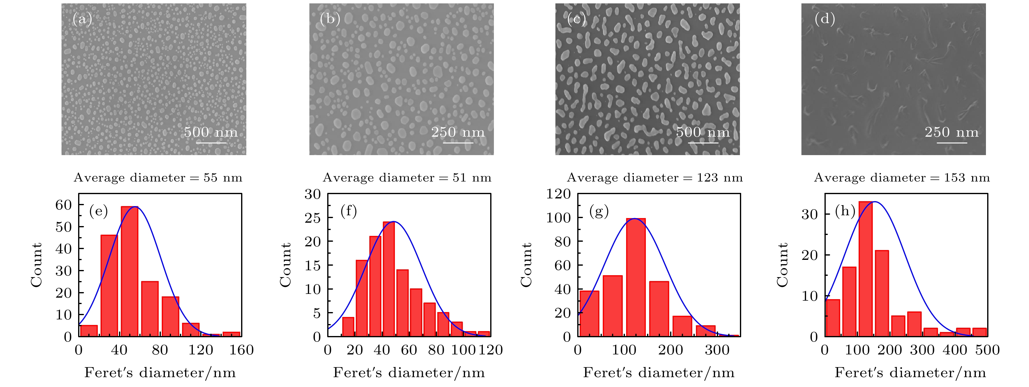
图 8 厚度为8 nm Au薄膜和Ag薄膜退火后的SEM图和粒径统计直方图 (a) Au退火700 ℃; (b) Au退火 900 ℃; (c) Ag退火 300 ℃; (d) Ag退火 700 ℃; (e)—(h) 相对应的粒径统计直方图结果
Fig. 8. SEM images and particle size statistical histograms of 8 nm thick Au films and Ag films after annealing: (a) Au annealed at 700 ℃; (b) Au annealed at 900 ℃; (c) Ag annealed at 300 ℃; (d) Ag annealed at 700 ℃; (e)–(h) corresponding particle size statistical histogram results.

图 9 VG与金属纳米颗粒结合前后的(a), (b)拉曼测试和(c), (d)光吸收率结果 (a), (c) VG与AgNPs; (b), (d) VG与AuNPs
Fig. 9. (a), (b) Raman and (c), (d) optical absorption results before and after the combination of VG and metal nanoparticles: (a), (c) VG with AgNPs; (b), (d) VG with AuNPs.
-
[1] Xia F, Mueller T, Lin Y, Valdes-Garcia A, Avouris P 2009 Nat. Nanotechnol. 4 839
Google Scholar
[2] Mittendorff M, Winnerl S, Kamann J, Eroms J, Weiss D, Schneider H, Helm M 2013 Appl. Phys. Lett. 103 021113
Google Scholar
[3] Compton O C, Nguyen S B T 2010 Small 6 711
Google Scholar
[4] Katsnelson M I 2007 Mater. Today 10 20
[5] Nair R R, Blake P, Grigorenko A N, Novoselov K S, Booth T J, Stauber T, Peres N M R, Geim A K 2008 Science 320 1308
Google Scholar
[6] Liu C, Chang Y, Norris T B, Zhong Z 2014 Nat. Nanotechnol. 9 273
Google Scholar
[7] Shi S F, Xu X, Ralph D C, McEuen P L 2011 Nano Lett. 11 1814
Google Scholar
[8] Emani N K, Chung T F, Ni X, Kildishev A V, Chen Y P, Boltasseva A 2012 Nano Lett. 12 5202
Google Scholar
[9] Lee H, Heo K, Park J, Park Y, Noh S, Kim K S, Lee C, Hong B H, Jian J, Hong S 2012 J. Mater. Chem. 22 8372
Google Scholar
[10] Babichev A V, Zhang H, Lavenus P, Julien F H, Egorov A Y, Lin Y T, Tu L W, Tchernycheva M 2013 Appl. Phys. Lett. 103 201103
Google Scholar
[11] Konstantatos G, Badioli M, Gaudreau L, Osmond J, Bernechea M, De Arquer P G F, Gatti F, Koppens F H 2012 Nat. Nanotechnol. 7 363
Google Scholar
[12] Bo Z, Yang Y, Chen J, Yu K, Yan J, Cen K 2013 Nanoscale 5 5180
Google Scholar
[13] Bo Z, Mao S, Han Z J, Cen K, Chen J, Ostrikov K K 2015 Chem. Soc. Rev. 44 2108
Google Scholar
[14] Zhu W, Xue Z Y, Wang G, Zhao M H, Chen D, Guo Q L, Liu Z D, Feng X Q, Ding G Q, Chu P K, Di Z F 2020 ACS Appl. Nano Mater. 3 6915
Google Scholar
[15] Yu K, Wang P, Lu G, Chen K H, Bo Z, Chen J 2011 J. Phys. Chem. Lett. 2 537
Google Scholar
[16] Graf A, Arndt M, Sauer M, Gerlach G 2007 Meas. Sci. Technol. 18 R59
Google Scholar
[17] Chaglla E J S, Celik N, Balachandran W 2018 Sensors 18 3315
Google Scholar
[18] Moisello E, Malcovati P, Bonizzoni E 2021 Micromachines 12 148
Google Scholar
[19] Buchner R, Sosna C, Maiwald M, Benecke W, Lang W 2006 Sens. Actuators, A 130 262
[20] Dijkstra M, Lammerink T S, de Boer M J, Berenschot E J W, Wiegerink R J, Elwenspoek M 2014 J. Microelectromech. Syst. 23 908
Google Scholar
[21] Randjelovic D, Petropoulos A, Kaltsas G, Stojanovic M, Lazic Z, Djuric Z, Matic M 2008 Sens. Actuators, A 141 404
Google Scholar
[22] Yoo K P, Hong H P, Lee M J, Min S J, Park C W, Choi W S, Min N K 2011 Meas. Sci. Technol. 22 115206
Google Scholar
[23] Itoigawa K, Ueno H, Shiozaki M, Toriyama T, Sugiyama S 2005 J. Micromech. Microeng. 15 S233
Google Scholar
[24] Dhawan R, Madusanka P, Hu G Y, Debord J, Tran T, Maggio K, Edwards H, Lee M 2020 Nat. Commun. 11 4362
Google Scholar
[25] Xu D H, Wang Y L, Xiong B, Li T 2017 Front. Mech. Eng. 12 557
Google Scholar
[26] Shahmarvandi E K, Ghaderi M, Wolffenbuttel R F 2016 J. Phys. Conf. Ser. 757 012033
Google Scholar
[27] Xu D, Xiong B, Wang Y 2010 IEEE Electron Device Lett. 31 512
Google Scholar
[28] Zhang C C, Mao H Y, Shi M, Xiong J J, Long K W, Chen D P 2020 33rd IEEE International Confence on Micro Electro Mechannical Systems (MEMS 2020) Vancouver, Canada, January 18–22, 2020 p949
[29] Qian F, Deng J, Xiong F, Dong Y, Xu C 2020 Opt. Mater. Express 10 2909
Google Scholar
[30] Li X, Zhu M, Du M, Lv Z, Zhang L, Li Y, Yang Y, Yang T, Li X, Wang K, Zhu Y, Fang Y 2016 Small 12 549
Google Scholar
[31] Tian W, Wang Y, Zhou H, Wang Y L, Li T 2020 J. Microelectromech Syst. 29 36
Google Scholar
[32] Sofiane B M, Sébastien E, Thomas B, Laurent T, Pascal V, Danick B, Jean-Paul G, Laurent C 2015 Microsyst. Technol. 21 1627
Google Scholar
[33] Allen L H, Patrick K H, Nathaniel M G, Sungjae H, Yong C S, Yi S, Matthew C, Madan D, Anantha P C, Jing K, Pablo J, Tomás P 2015 Nano Lett. 15 7211
Google Scholar
[34] Willets K A, Van Duyne, R P 2007 Ann. Rev. Phys. Chem. 58 267
Google Scholar

 下载:
下载:
计量
- 文章访问数: 5711
- PDF下载量: 106
- 被引次数: 0
