-
近年来, 石墨烯材料由于优异的光电性能获得了广泛关注, 并应用于发光二极管的透明电极以取代昂贵的铟锑氧化物(indium tin oxide, ITO)透明电极, 但由于石墨烯与p-GaN功函数不匹配, 二者很难形成好的欧姆接触, 因而造成器件电流扩展差和电压高等问题. 本文将ITO薄层作为石墨烯透明电极与p-GaN间的插入层, 以改善石墨烯与p-GaN层的欧姆接触. 所制备的石墨烯透明电极的方块电阻为252.6
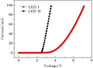
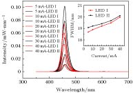
$ \Omega/\Box $ , 石墨烯/ITO复合透明电极的方块电阻为70.1$ \Omega/\Box $ ; 石墨烯透明电极与p-GaN层的比接触电阻率为1.92 × 10⁻² Ω·cm2, ITO插入之后, 其比接触电阻率降低为1.01 × 10⁻⁴ Ω·cm2; 基于石墨烯透明电极的发光二极管(light emitting diode, LED), 在20 mA注入电流下, 正向电压为4.84 V, 而石墨烯/ITO复合透明电极LED正向电压降低至2.80 V, 且光输出功率得到提高. 这归因于石墨烯/ITO复合透明电极与p-GaN界面处势垒高度的降低, 进而改善了欧姆接触; 另外, 方块电阻的降低, 使得电流扩展均匀性也得到了提高. 所采用的复合透明电极减少了ITO的用量, 得到了良好的欧姆接触, 为LED透明电极提供了一种可行方案.In recent years, graphene has received wide attention due to its excellent optoelectronic properties and has been applied to transparent electrodes of light-emitting diodes to replace the scarce and expensive indium antimony oxide (ITO), which is a typical current spreading layer in lateral GaN LED. However, there are some problems in graphene transparent electrode, such as the mismatch between graphene work function and p-GaN work function, and difficult-to-form good Ohmic contact with p-GaN, resulting in poor current expansion and high voltage of devices. In this paper, a thin ITO layer is used as an insertion layer between a three-layer graphene transparent electrode and and p-GaN, thereby improving the Ohmic contact between them. And a three-layer graphene/ITO composite transparent electrode LED is prepared and also compared with the pristine three-layer graphene LED. The thickness of ITO is only 50 nm, which is much thinner than the thickness of ITO in conventional LED. The sheet resistance of the prepared three-layer pristine graphene transparent electrode is 252.6$ \Omega/\Box $ , and the sheet resistance of the three-layer graphene/ITO composite transparent electrode is reduced to 70.1$ \Omega/\Box $ . The specific contact resistance between the three-layer pristine graphene transparent electrode and the p-GaN layer is 1.92 × 10⁻² Ω·cm2, after the ITO being inserted, the specific resistance is reduced to 1.01 × 10⁻⁴ Ω·cm2. Based on the three-layer graphene transparent electrode LED, the forward voltage is 4.84 V at an injection current of 20 mA, while the forward voltage of the three-layer graphene/ITO composite transparent electrode LED is reduced to 2.80 V; under small currents, the ideal factor of the three-layer graphene/ITO composite transparent electrode LED is less than that of the three-layer graphene transparent electrode LED. In addition, with the current increasing, the luminous intensity of the three-layer graphene/ITO composite transparent electrode LED increases, so does the radiant flux, which is because the addition of the ITO thin layer reduces the barrier height at the interface between the three layers of graphene and p-GaN, and the sheet resistance of the composite transparent electrode is also reduced, thereby improving the Ohmic contact between graphene and p-GaN. At the same time, the current spread is more uniform. The composite transparent electrode uses the much less ITO and obtains better optoelectronic performance, and thus providing a feasible solution for the LED transparent electrode.[1] Dupuis R D, Krames M R 2008 J. Lighwave Technol. 26 1154
 Google Scholar
[2] 郭道友, 李培刚, 陈政委, 吴真平, 唐为华 2019 物理学报 68 078501
 Google Scholar
Guo D Y, Li P G, Chen Z W, Wu Z P, Tang W H 2019 Acta Phys. Sin. 68 078501
 Google Scholar
[3] 黎振超, 陈梓铭, 邹广锐兴, 叶轩立, 曹镛 2019 物理学报 68 158505
 Google Scholar
Li Z C, Chen Z M, Zou G R X, Ye X L, Cao Y 2019 Acta Phys. Sin. 68 158505
 Google Scholar
[4] Kim B J, Yang G, Kim H Y, Baik K H, Mastro M A, Hite J K, Eddy C R, Ren F, Pearton S J, Kim J 2013 Opt. Express 21 29025
 Google Scholar
[5] Lee J M, Jeong H Y, Choi K J, Park W 2011 Appl. Phys. Lett. 99 41115
 Google Scholar
[6] Bonaccorso F, Sun Z, Hasan T, Ferrari A C 2010 Nature Photon. 4 611
 Google Scholar
[7] 蒲晓庆, 吴静, 郭强, 蔡建臻 2018 物理学报 67 217301
 Google Scholar
Pu X Q, Wu J, Guo Q, Cai J Z 2018 Acta Phys. Sin. 67 217301
 Google Scholar
[8] Seo T H, Kim S J, Kim M J, Kim H S, Suh E K 2014 J. Phys. D: Appl. Phys. 47 215103
 Google Scholar
[9] Wu C, Liu F, Liu B, Zhuang Z, Dai J P, Tao T, Zhang G, Xie Z L, Wang X R, Zhang R 2015 Solid State Electron. 109 47
 Google Scholar
[10] Xun K, Xie Y Y, Ma H L, Du Y X, Zeng F G, Ding P, Gao Z Y, Xu C, Sun J 2016 Solid State Electron. 126 5
 Google Scholar
[11] Youn D H, Yu Y J, Chio H K, Kim S K, Chio S Y, Chio C G 2013 Nanotechnology 24 075202
 Google Scholar
[12] Xu K, Xu C, Deng J, Zhu Y X, Guo W L, Mao M M, Zheng L Sun J 2013 Appl. Phys. Lett. 102 162102
 Google Scholar
[13] 甄聪棉, 李秀玲, 潘成福, 聂向富, 王印月 2005 大学物理 06 10
 Google Scholar
Zhen C M, Li X L, Pan C F, Nie C F, Wang Y Y 2005 College Phys. 06 10
 Google Scholar
[14] 马新宇, 陈茜, 廖杨芳, 肖清泉, 陈庆, 姚紫祎, 谢泉 2017 低温物理学报 39 16
 Google Scholar
Ma X Y, Chen X, Liao Y F, Xiao Q Q, Chen Q, Yao Z W, Xie Q 2017 Low Temp. Phys. Lett. 39 16
 Google Scholar
[15] 严光明, 李成, 汤梦饶, 黄诗浩, 王尘, 卢卫芳, 黄巍, 赖虹凯, 陈松岩 2013 物理学报 62 167304
 Google Scholar
Yan G M, Li C, Tang M R, Huang S H, Wang C, Lu W F, Huang W, Lai H K, Chen S Y 2013 Acta Phys. Sin. 62 167304
 Google Scholar
[16] 吴鼎芬, 颜本达 1989 金属-半导体界面欧姆接触的原理、测试与工艺 (上海: 上海交通大学出版社) 第36−39页
Wu D F, Yang B D 1989 Principle, Test and Process of Ohmic Contact at Metal-semiconductor Interface (Shanghai: Shanghai Jiaotong University Press) pp36−39 (in Chinese)
[17] Hao Y, Marc S, Tom S, Erik R, Koen M, Steven D, Naoto H, Kathy B, Nadine C, Kristin D M 2015 IEEE Electron Device Lett. 36 1
 Google Scholar
[18] Shah J M, Li Y L, Gessmann T, Schubert E F 2003 J. Appl. Phys. 94 2627
 Google Scholar
[19] 刘建朋, 朱彦旭, 郭伟玲, 闫微微, 吴国庆 2012 物理学报 61 137303
 Google Scholar
Liu J P, Zhu Y X, Guo W L, Yang W W, Wu G Q 2012 Acta Phys. Sin. 61 137303
 Google Scholar
[20] Guo X, Schubert E F 2001 Appl. Phys. Lett. 78 3337
 Google Scholar
[21] 吴晨晨, 郭相东, 胡海, 杨晓霞, 戴庆 2019 物理学报 68 148103
 Google Scholar
Wu C C, Guo X D, Hu H, Yang X X, Dai Q 2019 Acta Phys. Sin. 68 148103
 Google Scholar
-
图 1 制备的LED器件的结构示意图 (a)石墨烯透明电极LED I; (b)石墨烯/ITO复合透明电极LED II; (c)湿法转移石墨烯的光学显微镜图(左侧阴影部分为石墨烯, 右侧为ITO)
Fig. 1. Schematic diagram of the prepared LED device: (a) Graphene transparent electrode LED I; (b) graphene/ITO composite transparent electrode LED II; (c) optical micrograph of wet transfer graphene (graphene on the left and ITO on the right).
表 1 复合透明电极方块电阻及其与p-GaN比接触电阻率的测量结果
Table 1. Composite transparent electrode sheet resistance and its measurement results of contact resistivity with p-GaN.
透明电极类型 方块电阻 比接触电阻率 $R_{\rm sh}/ \Omega\cdot\Box^{-1}$ ρc/Ω·cm2 石墨烯 252.6 1.92 × 10⁻² 石墨烯/ITO 70.1 1.01 × 10⁻⁴ -
[1] Dupuis R D, Krames M R 2008 J. Lighwave Technol. 26 1154
 Google Scholar
[2] 郭道友, 李培刚, 陈政委, 吴真平, 唐为华 2019 物理学报 68 078501
 Google Scholar
Guo D Y, Li P G, Chen Z W, Wu Z P, Tang W H 2019 Acta Phys. Sin. 68 078501
 Google Scholar
[3] 黎振超, 陈梓铭, 邹广锐兴, 叶轩立, 曹镛 2019 物理学报 68 158505
 Google Scholar
Li Z C, Chen Z M, Zou G R X, Ye X L, Cao Y 2019 Acta Phys. Sin. 68 158505
 Google Scholar
[4] Kim B J, Yang G, Kim H Y, Baik K H, Mastro M A, Hite J K, Eddy C R, Ren F, Pearton S J, Kim J 2013 Opt. Express 21 29025
 Google Scholar
[5] Lee J M, Jeong H Y, Choi K J, Park W 2011 Appl. Phys. Lett. 99 41115
 Google Scholar
[6] Bonaccorso F, Sun Z, Hasan T, Ferrari A C 2010 Nature Photon. 4 611
 Google Scholar
[7] 蒲晓庆, 吴静, 郭强, 蔡建臻 2018 物理学报 67 217301
 Google Scholar
Pu X Q, Wu J, Guo Q, Cai J Z 2018 Acta Phys. Sin. 67 217301
 Google Scholar
[8] Seo T H, Kim S J, Kim M J, Kim H S, Suh E K 2014 J. Phys. D: Appl. Phys. 47 215103
 Google Scholar
[9] Wu C, Liu F, Liu B, Zhuang Z, Dai J P, Tao T, Zhang G, Xie Z L, Wang X R, Zhang R 2015 Solid State Electron. 109 47
 Google Scholar
[10] Xun K, Xie Y Y, Ma H L, Du Y X, Zeng F G, Ding P, Gao Z Y, Xu C, Sun J 2016 Solid State Electron. 126 5
 Google Scholar
[11] Youn D H, Yu Y J, Chio H K, Kim S K, Chio S Y, Chio C G 2013 Nanotechnology 24 075202
 Google Scholar
[12] Xu K, Xu C, Deng J, Zhu Y X, Guo W L, Mao M M, Zheng L Sun J 2013 Appl. Phys. Lett. 102 162102
 Google Scholar
[13] 甄聪棉, 李秀玲, 潘成福, 聂向富, 王印月 2005 大学物理 06 10
 Google Scholar
Zhen C M, Li X L, Pan C F, Nie C F, Wang Y Y 2005 College Phys. 06 10
 Google Scholar
[14] 马新宇, 陈茜, 廖杨芳, 肖清泉, 陈庆, 姚紫祎, 谢泉 2017 低温物理学报 39 16
 Google Scholar
Ma X Y, Chen X, Liao Y F, Xiao Q Q, Chen Q, Yao Z W, Xie Q 2017 Low Temp. Phys. Lett. 39 16
 Google Scholar
[15] 严光明, 李成, 汤梦饶, 黄诗浩, 王尘, 卢卫芳, 黄巍, 赖虹凯, 陈松岩 2013 物理学报 62 167304
 Google Scholar
Yan G M, Li C, Tang M R, Huang S H, Wang C, Lu W F, Huang W, Lai H K, Chen S Y 2013 Acta Phys. Sin. 62 167304
 Google Scholar
[16] 吴鼎芬, 颜本达 1989 金属-半导体界面欧姆接触的原理、测试与工艺 (上海: 上海交通大学出版社) 第36−39页
Wu D F, Yang B D 1989 Principle, Test and Process of Ohmic Contact at Metal-semiconductor Interface (Shanghai: Shanghai Jiaotong University Press) pp36−39 (in Chinese)
[17] Hao Y, Marc S, Tom S, Erik R, Koen M, Steven D, Naoto H, Kathy B, Nadine C, Kristin D M 2015 IEEE Electron Device Lett. 36 1
 Google Scholar
[18] Shah J M, Li Y L, Gessmann T, Schubert E F 2003 J. Appl. Phys. 94 2627
 Google Scholar
[19] 刘建朋, 朱彦旭, 郭伟玲, 闫微微, 吴国庆 2012 物理学报 61 137303
 Google Scholar
Liu J P, Zhu Y X, Guo W L, Yang W W, Wu G Q 2012 Acta Phys. Sin. 61 137303
 Google Scholar
[20] Guo X, Schubert E F 2001 Appl. Phys. Lett. 78 3337
 Google Scholar
[21] 吴晨晨, 郭相东, 胡海, 杨晓霞, 戴庆 2019 物理学报 68 148103
 Google Scholar
Wu C C, Guo X D, Hu H, Yang X X, Dai Q 2019 Acta Phys. Sin. 68 148103
 Google Scholar
计量
- 文章访问数: 14641
- PDF下载量: 135
- 被引次数: 0


 下载:
下载:


