


-
基于F离子注入隔离技术实现一种新型微缩化发光二极管(micromicro-LED)阵列器件, 并系统研究注入能量及发光孔径对micro-LED阵列器光电性能的影响. 研究结果表明: 相比于F离子50 keV单次注入器件, 50/100 keV两次注入器件具有更好的光电性能, 器件反向漏电降低8.4倍, 光输出功率密度提升1.3倍. 同时, 在不同的发光孔径(6, 8, 10 μm)条件下, 器件反向漏电流均为3.4×10⁻⁸ A, 但正向工作电压随孔径增大而减小, 分别为3.3, 3.1, 2.9 V. 此外, 器件不同发光孔径的有效发光面积比(实际发光面积与器件面积之比)分别为85%, 87%, 92%. 与传统台面刻蚀micro-LED器件相比, 离子注入隔离技术实现的micro-LED器件具有较低反的向漏电流密度、较高的光输出密度及有效发光面积比.
-
关键词:
- 微缩化发光二极管阵列 /
- 离子注入隔离 /
- 注入能量 /
- 发光孔径
Compared with conventional light-emitting diode (LED), micro-LED has excellent photo-electric properties such as high current density, light output power density, light response frequency. It has widespread application prospects in the field of light display, optical tweezers, and visible light communication. However, dry etching inevitably leads the sidewall to be damaged, which results in the degradation of device properties. In this letter, a micro-LED array device based on F ions implantation isolation technology is presented to avoid damaging the sidewall. We systemically investigate the influence of fluorine ion implantation energy and light-emitting apertures on the photoelectric properties of the micro-LED array device by testing the current-voltage characteristic and light output power. The investigation results show that comparing with F ion 50 keV single implantation device, the reverse leakage of 50/100 keV double implantation device decreases by 8.4 times and the optical output density increases by 1.3 times. When the light-emitting apertures are different (6, 8, 10 μm respectively), the reverse leakage current remains constant, and the forward operating voltage decreasesfrom 3.3 V to 3.1 V and to 2.9 V with the increase of the aperture. Besides, the available area ratio, i.e. the ratio of actual light-emitting area to device area of single micro-LED with different light-emitting apertures are 85%, 87%, and 92%, respectively. The electrical isolation of the micro-LED array is realized by ion implantation isolation technology, and the micro-LED has some advantages over the conventional mesa etching micro-LED device, such as low reverse leakage current density, high optical output power density, and high effective light-emitting area ratio.-
Keywords:
- micro-light-emitting diode /
- ion implantation isolation /
- implantation energy /
- emission aperture
[1] Zhang L, Ou F, Chong W C, Chen Y J, Li Q M 2018 J. Soc. Inf. Disp. 26 137
 Google Scholar
[2] Day J, Li J, Lie D Y C, Bradford C, Y. Lin J, Jiang H X 2011 Appl. Phys. Lett. 99 031116
Google Scholar
[3] Zhang X, Li P A, Zou X B, Jiang J M, Yuen S H, Tang C W, Lau K M 2019 IEEE Photonics Technol. Lett. 31 865
Google Scholar
[4] Xie E Y, He X Y, Islim M S, Purwita A A, McKendry J J D, Gu E, Haas H, Dawson M D 2019 J. Lightwave Technol. 37 1180
Google Scholar
[5] Alicja Z D, Steven L N, David M, Jonathan M, Bruce R R, Robert K H, Mervyn J R, Huabing Y, Jonathan M C, Erdan G, Martin D D 2011 Opt. Express 19 3
[6] McAlinden N, Massoubre D, Richardson E, Gu E, Sakata S, Dawson M D, Mathieson K 2013 Opt. Lett. 38 992
Google Scholar
[7] 郭建新, 郭海成 2000 物理学报 49 1995
Guo J X, Kwok H S 2000 Acta Phys. Sin. 49 1995
[8] Komoda T, Sasabe H, Kido J 2018 25th International Workshop on Active-Matrix Flatpanel Displays and Devices (AM-FPD) Kyoto, Japan, July 3–6, 2018 p978
[9] 何家琪, 何大伟, 王永生, 刘智勇 2013 物理学报 62 178801
Google Scholar
He J Q, He D W, Wang Y S, Liu Z Y 2013 Acta Phys. Sin. 62 178801
Google Scholar
[10] Son K R, Lee T H, Lee B R, Im H S, Kim T G 2018 Small 14 1801032
Google Scholar
[11] Li P, Zhao Y, Li H, Li Z, Zhang Y, Kang J, Liang M, Liu Z, Yi X, Wang G 2019 Nanotechnology 30 095203
Google Scholar
[12] Chen C J, Chen H C, Liao J Hao, Yu C J, Wu M C 2019 IEEE J. Quantum Electron. 55 2
Google Scholar
[13] 班章, 梁静秋, 吕金光, 梁中翥, 冯思悦 2013 物理学报 67 070701
Google Scholar
Ban Z, Liang J Q, Lv J G, Liang Z Z, Feng S Y 2013 Acta Phys. Sin. 67 070701
Google Scholar
[14] Jin S X, Li J, Li J Z, Lin J Y, Jiang H X 1999 Appl. Phys. Lett. 76 631
[15] 龚欣, 吕玲, 郝跃, 李培咸, 周小伟, 陈海峰 2007 半导体学报 28 7
Gong X, Lv L, Hao Y, Li P X, Zhou X W, Chen H F 2007 Chin. J. Semiconductors 28 7
[16] Kou J Q, Shen C C, Shao H, Che J M, Hou X, Chu C S, Tian K K, Zhang Y G, Zhang Z H, Kuo H C 2019 Opt. Express 27 643
Google Scholar
[17] Olivier F, Tirano S, Dupre L, Aventurier B, Largeron C, Templier F Spring Meeting of the European-Materials-Research-Society (E-MRS)/Symposium M on Silicon Compatible Materials and Integrated Devices for Photonics and Optical Sensing Lille, FRANCE, MAY 02–06, 2016 p191
[18] Tian P F, McKendry J J D, Zheng G, Guilhabert B, Watson I M, Gu E, Chen Z Z, Zhang G Y, Dawson M D 2012 Appl. Phys. Lett. 101 23
[19] Hwang D, Mughal A, Pynn C D, Nakamura S, DenBaars S P 2017 Appl. Phys. Express 10 032101
Google Scholar
[20] 张志利 2017 博士学位论文 (合肥: 中国科学院大学)
Zhang Z L 2017 Ph. D. Dissertation (Hefei: University of Chinese Academy of Sciences) (in Chinese)
[21] Pearton S J, Abernathy C R, Vartuli C B 1995 Appl. Phys. Lett. 66 3042
Google Scholar
[22] Kucheyeva S O, Williamsa J S, Peartonb S J 2001 Mater. Sci. Eng. R-Rep. 33 51
Google Scholar
[23] Dupre L, Marra M, Verney V, Aventurier B, Henry F, Olivier F, Tirano S, Daami A, Templier F Conference on Gallium Nitride Materials and Devices XII San Francisco, CA, JAN 30–FEB 02, 2017 p1010422-1
[24] Li C C, Zhan J L, Chen Z Z, Jiao F, Chen Y F, Chen Y Y, Nie J X, Kang X N, Li S F, Wang Q, Zhang G Y, Shen B 2019 Opt. Express 27 A1146
Google Scholar
[25] Wong M S, Hwang D, Alhassan A I, Lee C, Ley R, Nakamura S, DenBaars S P 2018 Opt. Express 26 21324
Google Scholar
[26] Choi H W, Jeon C W, Dawson M D, Edwards P R, Martin R W, Tripathy S 2003 J. Appl. Phys. 93 5978
Google Scholar
[27] Gong Z, Massoubre D, McKendry J, Zhang H X, Griffin C, Guilhabert B, Gu E, Girkin J M, Dawson M D, Rael B R, Henderson R K International Workshop on Nitride Semiconductors Montreux, SWITZERLAND, OCT 06–10, 2008 p6
[28] Xie E Y, Stonehouse M, Ferreira R, McKendry J J D, Herrnsdorf J, He X, Rajbhandari S, Chun H, Jalajakumari A V N, Almer O, Faulkner G, Watson I M, Gu E, Henderson Robert, O’Brien D, Dawson M D 2017 IEEE Photonics J. 9 1
[29] Chen C J, Chen H C, Liao J H, Yu C J, Wu M C 2019 IEEE J. Quantum Electron. 55 1
[30] Stoller R E, Toloczko M B, Was G S, Certain A G, Dwaraknath S, Garner F A 2013 Nucl. Instrum. Methods Phys. Res. Sect. B-Beam Interact. Mater. Atoms 310 75
Google Scholar
-
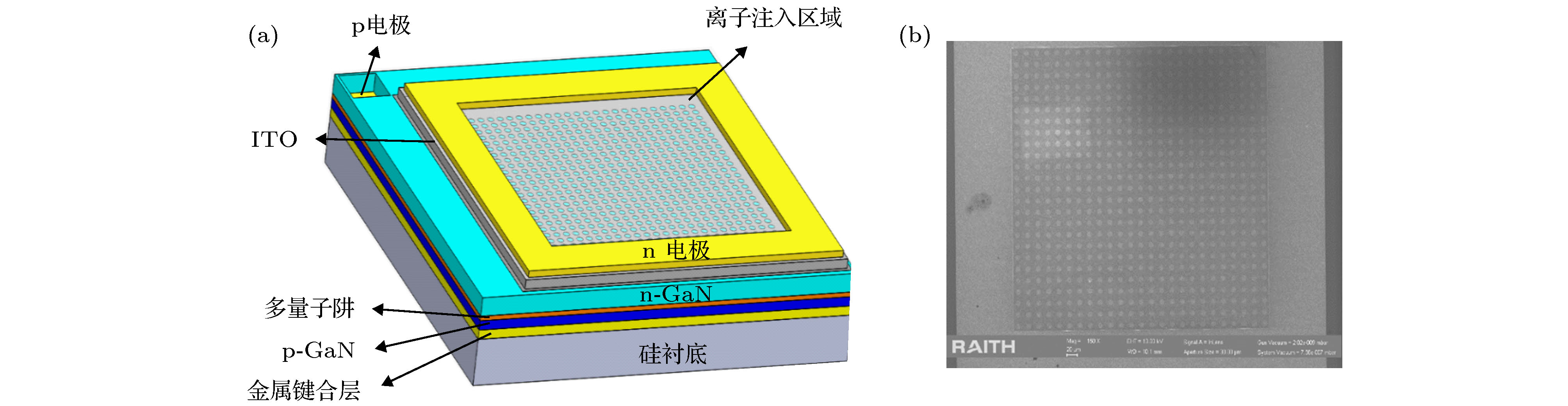
图 1 (a) micro-LED阵列结构图; (b) 10 μm micro-LED阵列表面SEM图像
Fig. 1. (a) Schematic structure of micro-LED array; (b) SEM image of 10 μm micro-LED array surface.
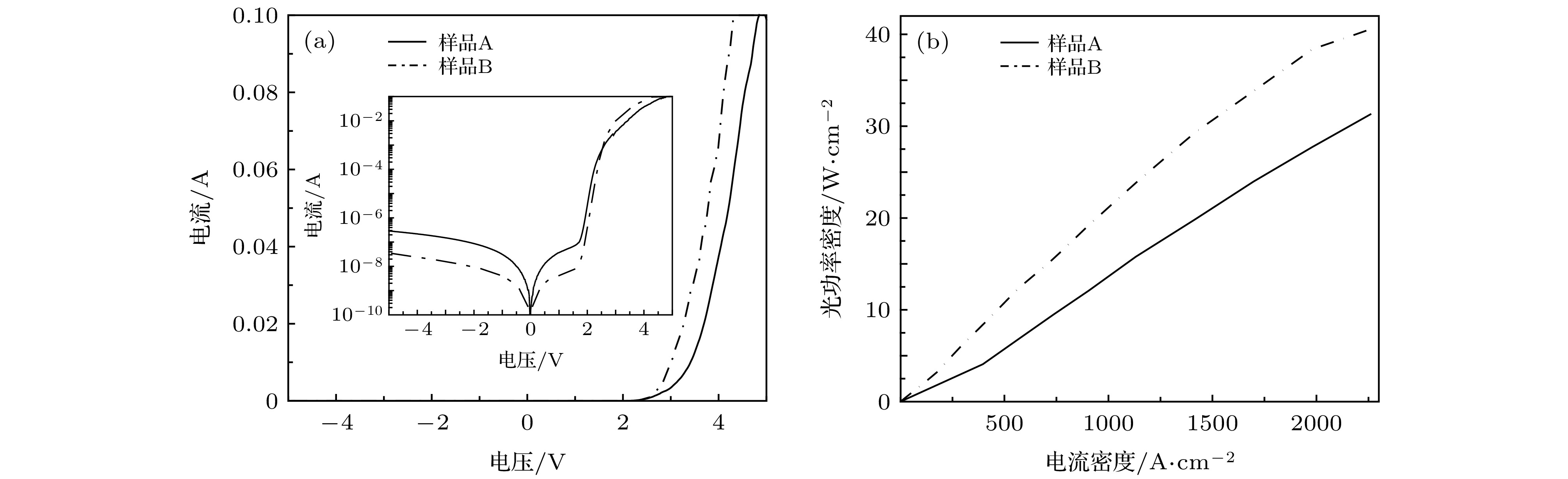
图 2 样品A和B 6 μm阵列的(a) I-V 特性和(b)光输出密度-电流密度特性
Fig. 2. (a) The I-V and (b) light output power density-current density characteristics of 6 μm arrays of samples A and B
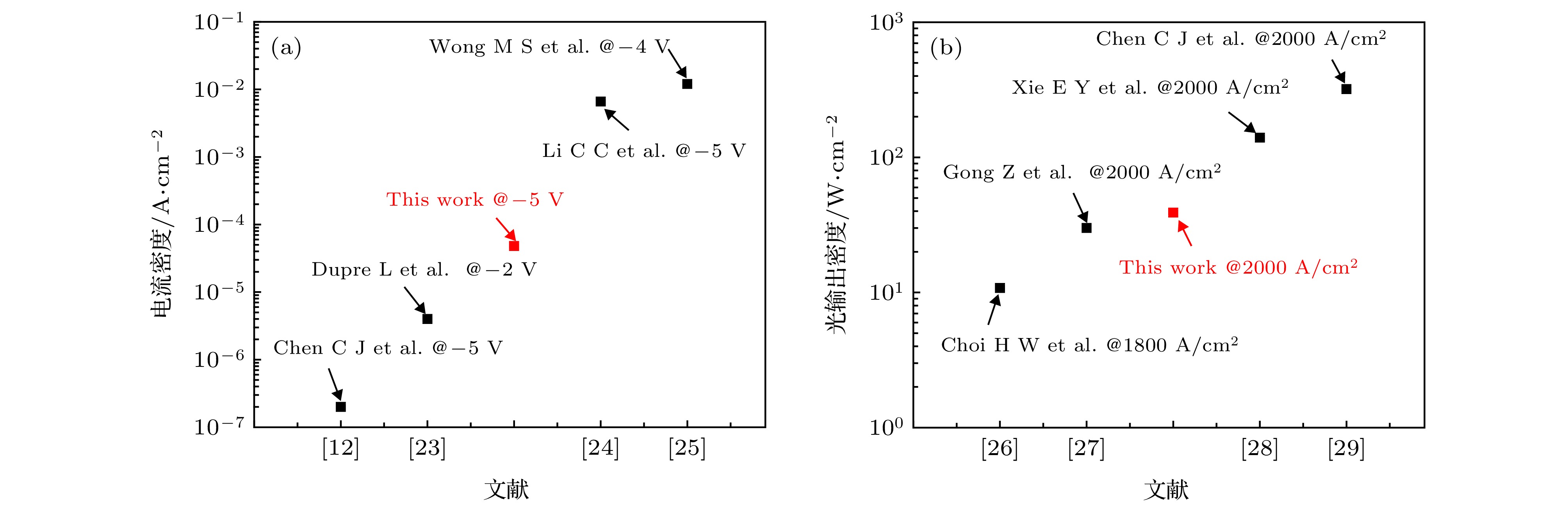
图 3 注入隔离micro-LED器件与台面刻蚀器件 (a)反向漏电流和(b)光输出密度比较
Fig. 3. Comparison of (a) reverse leakage current and (b) light output density between implanted isolated micro-LED devices and mesa etching devices.

图 4 SRIM模拟F离子不同注入能量下产生的损伤与注入深度关系
Fig. 4. The relationship between damage and implantation depth of F ion with different implantation energies with SRIM simulation.
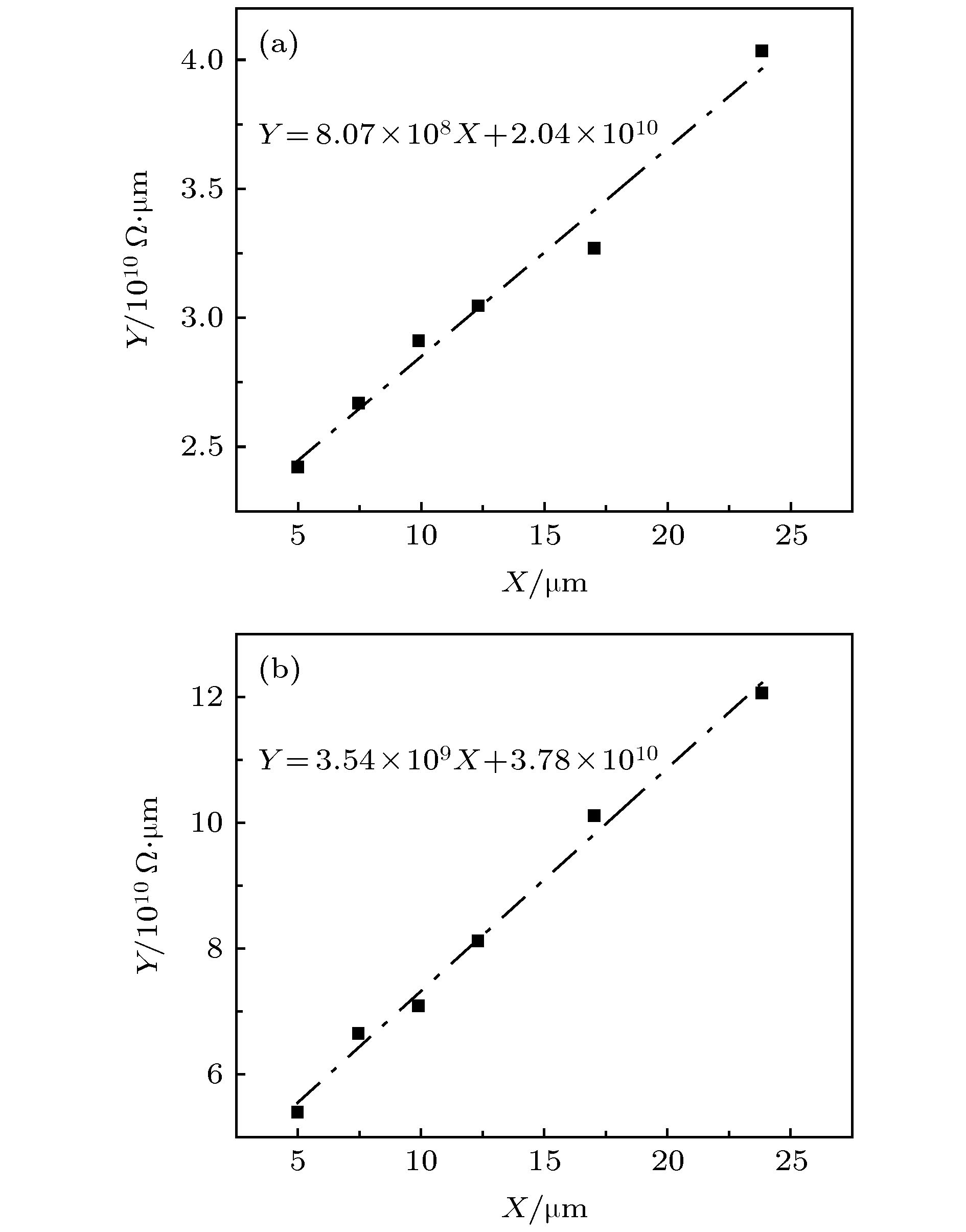
图 6 CTLM线性拟合曲线 (a) 50 keV能量注入; (b) 50/100 keV能量注入
Fig. 6. The CTLM linear fitting curve at (a) the implantation energy of 50 keV and (b) 50/100 keV.
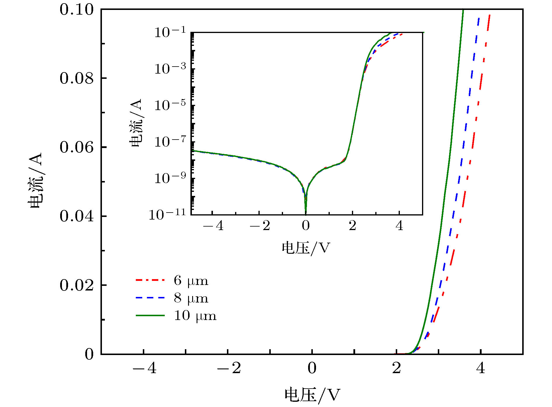
图 7 不同发光孔径阵列I-V特性曲线
Fig. 7. I-V characteristics of the different emission aperture arrays.
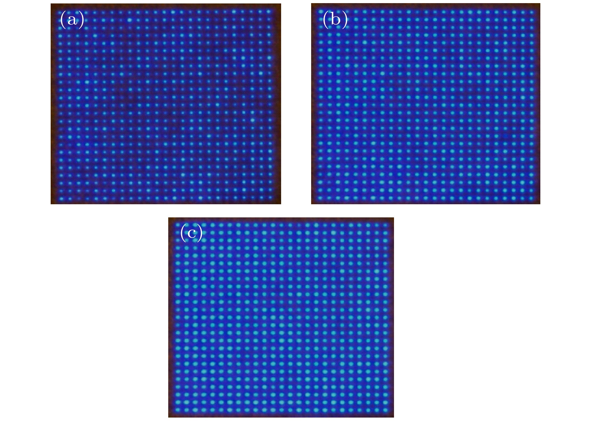
图 8 20 mA下 (a) 6 μm, (b) 8 μm, (c) 10 μm发光孔径阵列发光图像
Fig. 8. Light-emitting aperture arrays of (a) 6 μm, (b) 8 μm, and (c)10 μm at 20 mA.
表 1 6 μm micro-LED阵列光电性能参数
Table 1. The photoelectric properties of 6 μm micro-LED array.
样品 工作电压(20 mA)/V 反向漏电流(–5 V)/A 光输出密度(2264 A/cm–2)/W·cm–2 A 3.69 2.89 × 10⁻⁷ 31.34 B 3.27 3.43 × 10⁻⁸ 40.59  下载: 导出CSV
-
[1] Zhang L, Ou F, Chong W C, Chen Y J, Li Q M 2018 J. Soc. Inf. Disp. 26 137
Google Scholar
[2] Day J, Li J, Lie D Y C, Bradford C, Y. Lin J, Jiang H X 2011 Appl. Phys. Lett. 99 031116
Google Scholar
[3] Zhang X, Li P A, Zou X B, Jiang J M, Yuen S H, Tang C W, Lau K M 2019 IEEE Photonics Technol. Lett. 31 865
Google Scholar
[4] Xie E Y, He X Y, Islim M S, Purwita A A, McKendry J J D, Gu E, Haas H, Dawson M D 2019 J. Lightwave Technol. 37 1180
Google Scholar
[5] Alicja Z D, Steven L N, David M, Jonathan M, Bruce R R, Robert K H, Mervyn J R, Huabing Y, Jonathan M C, Erdan G, Martin D D 2011 Opt. Express 19 3
[6] McAlinden N, Massoubre D, Richardson E, Gu E, Sakata S, Dawson M D, Mathieson K 2013 Opt. Lett. 38 992
Google Scholar
[7] 郭建新, 郭海成 2000 物理学报 49 1995
Guo J X, Kwok H S 2000 Acta Phys. Sin. 49 1995
[8] Komoda T, Sasabe H, Kido J 2018 25th International Workshop on Active-Matrix Flatpanel Displays and Devices (AM-FPD) Kyoto, Japan, July 3–6, 2018 p978
[9] 何家琪, 何大伟, 王永生, 刘智勇 2013 物理学报 62 178801
Google Scholar
He J Q, He D W, Wang Y S, Liu Z Y 2013 Acta Phys. Sin. 62 178801
Google Scholar
[10] Son K R, Lee T H, Lee B R, Im H S, Kim T G 2018 Small 14 1801032
Google Scholar
[11] Li P, Zhao Y, Li H, Li Z, Zhang Y, Kang J, Liang M, Liu Z, Yi X, Wang G 2019 Nanotechnology 30 095203
Google Scholar
[12] Chen C J, Chen H C, Liao J Hao, Yu C J, Wu M C 2019 IEEE J. Quantum Electron. 55 2
Google Scholar
[13] 班章, 梁静秋, 吕金光, 梁中翥, 冯思悦 2013 物理学报 67 070701
Google Scholar
Ban Z, Liang J Q, Lv J G, Liang Z Z, Feng S Y 2013 Acta Phys. Sin. 67 070701
Google Scholar
[14] Jin S X, Li J, Li J Z, Lin J Y, Jiang H X 1999 Appl. Phys. Lett. 76 631
[15] 龚欣, 吕玲, 郝跃, 李培咸, 周小伟, 陈海峰 2007 半导体学报 28 7
Gong X, Lv L, Hao Y, Li P X, Zhou X W, Chen H F 2007 Chin. J. Semiconductors 28 7
[16] Kou J Q, Shen C C, Shao H, Che J M, Hou X, Chu C S, Tian K K, Zhang Y G, Zhang Z H, Kuo H C 2019 Opt. Express 27 643
Google Scholar
[17] Olivier F, Tirano S, Dupre L, Aventurier B, Largeron C, Templier F Spring Meeting of the European-Materials-Research-Society (E-MRS)/Symposium M on Silicon Compatible Materials and Integrated Devices for Photonics and Optical Sensing Lille, FRANCE, MAY 02–06, 2016 p191
[18] Tian P F, McKendry J J D, Zheng G, Guilhabert B, Watson I M, Gu E, Chen Z Z, Zhang G Y, Dawson M D 2012 Appl. Phys. Lett. 101 23
[19] Hwang D, Mughal A, Pynn C D, Nakamura S, DenBaars S P 2017 Appl. Phys. Express 10 032101
Google Scholar
[20] 张志利 2017 博士学位论文 (合肥: 中国科学院大学)
Zhang Z L 2017 Ph. D. Dissertation (Hefei: University of Chinese Academy of Sciences) (in Chinese)
[21] Pearton S J, Abernathy C R, Vartuli C B 1995 Appl. Phys. Lett. 66 3042
Google Scholar
[22] Kucheyeva S O, Williamsa J S, Peartonb S J 2001 Mater. Sci. Eng. R-Rep. 33 51
Google Scholar
[23] Dupre L, Marra M, Verney V, Aventurier B, Henry F, Olivier F, Tirano S, Daami A, Templier F Conference on Gallium Nitride Materials and Devices XII San Francisco, CA, JAN 30–FEB 02, 2017 p1010422-1
[24] Li C C, Zhan J L, Chen Z Z, Jiao F, Chen Y F, Chen Y Y, Nie J X, Kang X N, Li S F, Wang Q, Zhang G Y, Shen B 2019 Opt. Express 27 A1146
Google Scholar
[25] Wong M S, Hwang D, Alhassan A I, Lee C, Ley R, Nakamura S, DenBaars S P 2018 Opt. Express 26 21324
Google Scholar
[26] Choi H W, Jeon C W, Dawson M D, Edwards P R, Martin R W, Tripathy S 2003 J. Appl. Phys. 93 5978
Google Scholar
[27] Gong Z, Massoubre D, McKendry J, Zhang H X, Griffin C, Guilhabert B, Gu E, Girkin J M, Dawson M D, Rael B R, Henderson R K International Workshop on Nitride Semiconductors Montreux, SWITZERLAND, OCT 06–10, 2008 p6
[28] Xie E Y, Stonehouse M, Ferreira R, McKendry J J D, Herrnsdorf J, He X, Rajbhandari S, Chun H, Jalajakumari A V N, Almer O, Faulkner G, Watson I M, Gu E, Henderson Robert, O’Brien D, Dawson M D 2017 IEEE Photonics J. 9 1
[29] Chen C J, Chen H C, Liao J H, Yu C J, Wu M C 2019 IEEE J. Quantum Electron. 55 1
[30] Stoller R E, Toloczko M B, Was G S, Certain A G, Dwaraknath S, Garner F A 2013 Nucl. Instrum. Methods Phys. Res. Sect. B-Beam Interact. Mater. Atoms 310 75
Google Scholar

 下载:
下载:

计量
- 文章访问数: 15979
- PDF下载量: 271
- 被引次数: 0
