-
AlGaN/GaN界面处的二维电子气迁移率是描述高电子迁移率晶体管特性的一个重要参数, 极化光学声子散射是高温时限制二维电子气迁移率的主要散射机制. 本文对极化光学声子散射进行计算, 结果表明在二维电子气浓度为6 × 10¹¹—1 × 1013 cm–2, 温度为200—400 K范围内, 极化光学声子散射因素决定的迁移率随温度的变化近似为
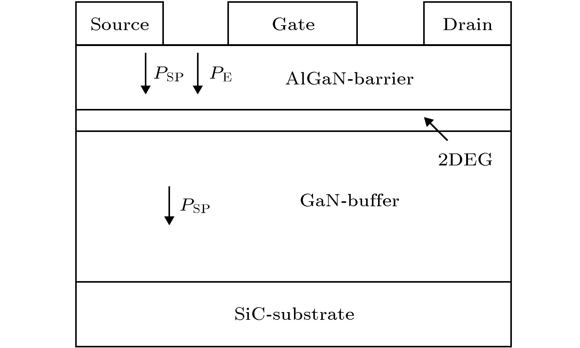
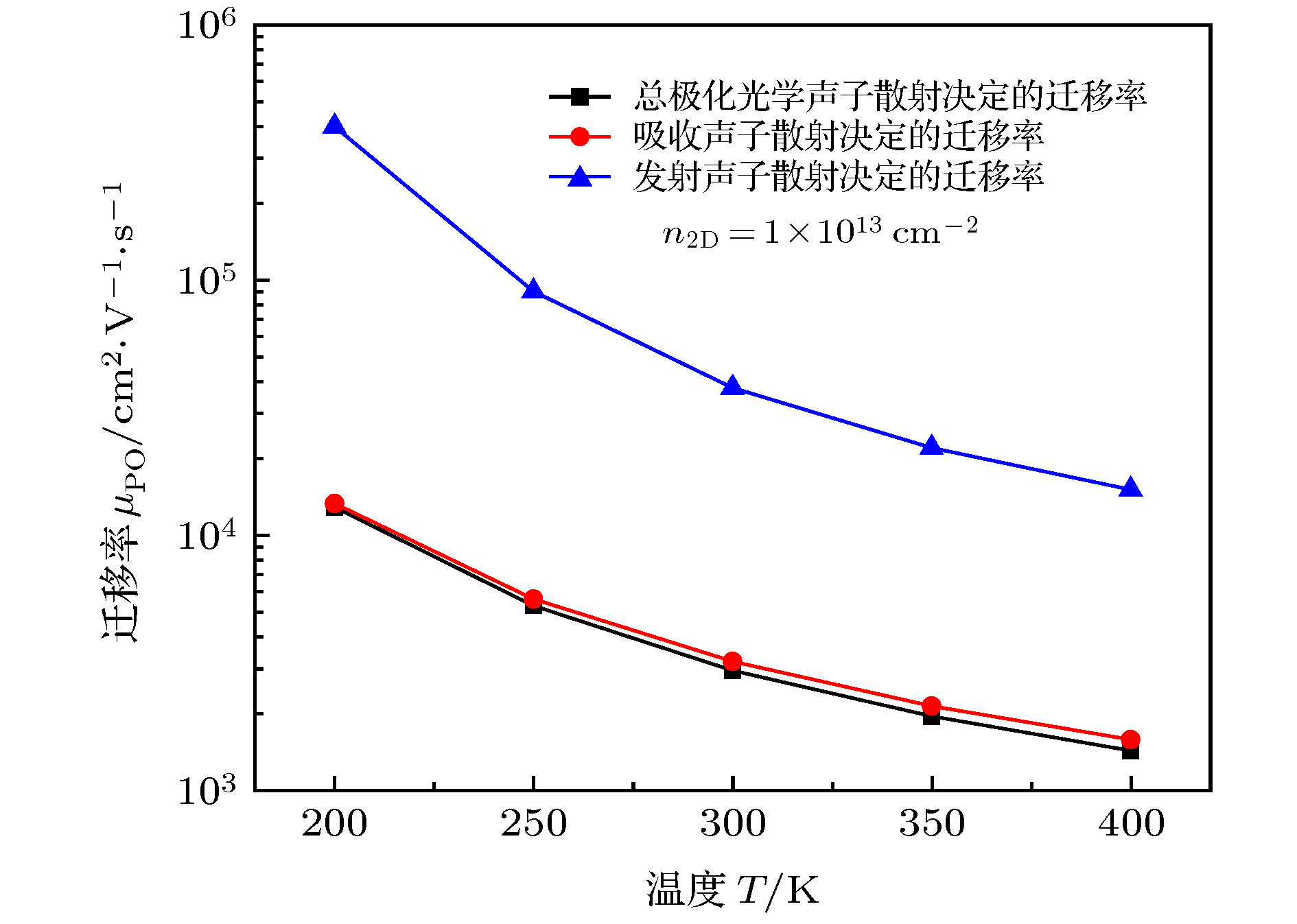
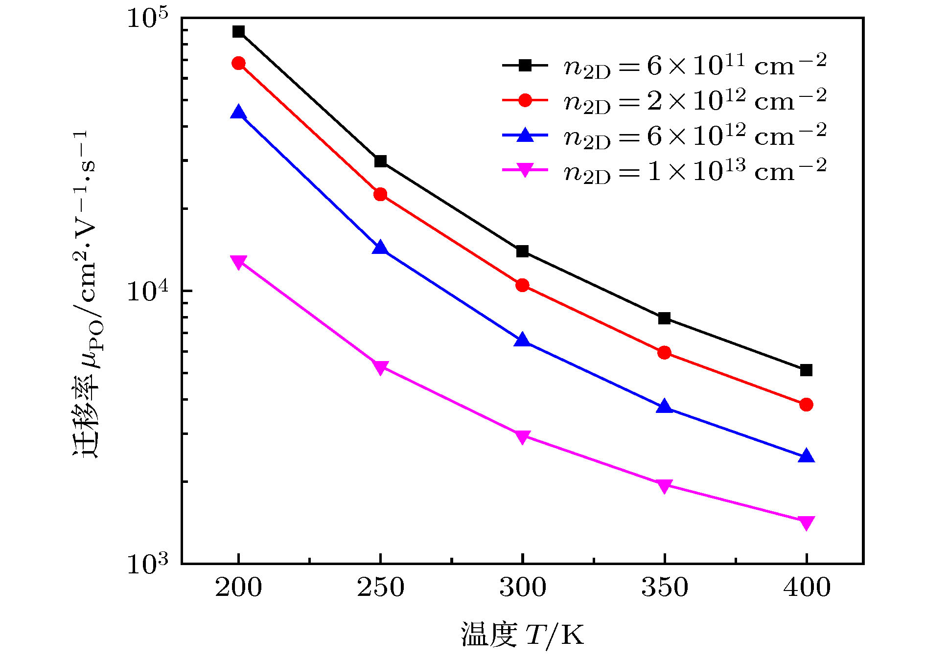
$ \mu_{\rm PO} = AT^{-\alpha} ~ (\alpha = 3.5) $ ; 由于GaN中光学声子能量较大, 吸收声子对迁移率的影响远大于发射声子的影响. 进一步讨论了极化光学声子散射因素决定的迁移率随光学声子能量变化的趋势, 表明增加极化光学声子能量可提高二维电子气的室温迁移率.With the increasing demand for high-frequency, high-power and high-temperature microwave applications, AlGaN/GaN high electron mobility transistors have received much attention due to their promising material features such as wide band gaps, high-concentration two-dimensional electron gas (2DEG), strong electric field, at which the electron velocity is saturated, and high operating temperature. The 2DEG mobility at AlGaN/GaN interface is a key parameter to describe characteristics of high electron mobility transistor, and the mobility of 2DEG in AlGaN/GaN high electron mobility transistor is determined by a variety of scattering mechanisms in which the polar optical phonon scattering caused by electrostatic field between uneven polar positive and negative charges is responsible for mobility limitation in a 2DEG at high temperature. Calculation of polar optical phonon scattering is carried out by the analytical model in which Fang-Howard variational wave function and Fermi’s golden rule are used. The interaction between 2DEG and phonon is described by scattering matrix element for the transition, in which phonon occupation number is given by Bose-Einstein statistics. The scattering time is derived by neglecting the in-scattering, and the numerically calculated energy-dependent scattering time is averaged according to Fermi statistics. At temperatures in a range of 200–400 K and two-dimensional electron gas concentration in a range of 6 × 10¹¹–1 × 1013 cm–2, the mobility varying with temperature is analyzed. It is found that the mobility limited by polar phonon scattering decreases monotonically with the temperature rising and their dependence is well approximated by a function of $\mu_{\rm PO} = AT^{-\alpha} ~ (\alpha = 3.5)$ as the phonon occupation number increases with temperature rising. Furthermore, the polar optical phonon scattering is enhanced by greater electron concentration as a result of increased interaction between phonon and 2DEG. The mobility limit is calculated separately by emission phonon and absorption phonon, the results indicate that absorption phonon is predominant, which is attributed to high optical phonon energy in GaN. The mobility of polar optical phonon scattering is further studied by changing the optical phonon energy, which shows that the room temperature mobility of 2DEG can be improved by increasing the energy of polar optical phonon.-
Keywords:
- two-dimensional electron gas /
- polar optical phonon scattering /
- high temperature mobility /
- optical phonon energy
[1] Yu E T, Dang X Z, Asbeck P M, Lau S S, Sullivan G J 1999 J. Vac. Sci. Technol., B 17 1742
 Google Scholar
[2] Ji D, Liu B, Lu Y W, Zou M, Fan B L 2012 Chin. Phys. B 21 067201
 Google Scholar
[3] Ibbetson J P, Fini P T, Ness K D, DenBaars S P, Speck J S, Mishra U K 2000 Appl. Phys. Lett. 77 250
 Google Scholar
[4] 刘贵鹏 2013 博士学位论文 (北京: 中国科学院大学)
Liu G P 2013 Ph. D. Dissertation (Beijing: University of Chinese Academy of Sciences) (in Chinese)
[5] Hsu L, Walukiewicz W 1997 Phys. Rev. B 56 1520
 Google Scholar
[6] Gokden S 2003 Phys. Status Solidi A 200 369
 Google Scholar
[7] Anderson D R, Zakhleniuk N A, Babiker M, Ridley B K, Bennett C R 2001 Phys. Rev. B 63 245313
 Google Scholar
[8] Ridley B K 1998 J. Phys. Condens. Matter 10 6717
 Google Scholar
[9] 张金凤, 郝跃, 张进城, 倪金玉 2008 中国科学E辑: 信息科学 38 949
Zhang J F, Hao Y, Zhang J C, Ni J Y 2008 Sci. China Ser. E: Inf. Sci. 38 949
[10] 杨福军, 班士良 2012 物理学报 61 087201
 Google Scholar
Yang F J, Ban S L 2012 Acta Phys. Sin. 61 087201
 Google Scholar
[11] Protasov D Y, Malin T V, Tikhonov A V, Tsatsulnikov A F, Zhuravlev K S 2013 Semiconductors 47 33
 Google Scholar
[12] 陈志凯 2016 博士学位论文 (成都: 电子科技大学)
Chen Z K 2016 Ph. D. Dissertation (Chengdu: University of Electronic Science and Technology of China) (in Chinese)
[13] 杨鹏, 吕燕伍, 王鑫波 2015 物理学报 64 197303
 Google Scholar
Yang P, Lü Y W, Wang X B 2015 Acta Phys. Sin. 64 197303
 Google Scholar
[14] Gurusinghe M N, Davidsson S K, Andersson T G 2005 Phys. Rev. B 72 045316
 Google Scholar
[15] Rode D L 1975 Semiconductors and Semimetals (New York: Academic Press) pp4–28
[16] Yokoyama K, Hess K 1986 Phys. Rev. B 33 5595
 Google Scholar
[17] Price P J 1981 Ann. Phys. 133 217
 Google Scholar
[18] Look D C, Sizelove J R, Keller S, Wu Y F, Mishra U K, DenBaars S P 1997 Solid State Commun. 102 297
 Google Scholar
[19] Chin V W L, Tansley T L, Osotchan T 1994 J. Appl. Phys. 75 7365
 Google Scholar
[20] Cui P, Mo J H, Fu C, Lü Y J, Liu H, Cheng A J, Luan C B, Zhou Y, Dai G, Lin Z J 2018 Sci. Rep. 8 9036
[21] Ambacher O, Smart J, Shealy J R, Weimann N G, Chu K, Murphy M, Schaff W J, Eastman L F, Dimitrov R, Wittmer L, Stutzmann M, Rieger W, Hilsenbeck J 1999 J. Appl. Phys. 85 3222
 Google Scholar
[22] Zhang Y F, Smorchkova I P, Elsass C R, Keller S, Ibbetson J P, Denbaars S, Mishra U K, Singh J 2000 J. Appl. Phys. 87 7981
 Google Scholar
[23] Zhao D G, Xu S J, Xie M H, Tong S Y, Yang H 2003 Appl. Phys. Lett. 83 677
 Google Scholar
-
-
[1] Yu E T, Dang X Z, Asbeck P M, Lau S S, Sullivan G J 1999 J. Vac. Sci. Technol., B 17 1742
 Google Scholar
[2] Ji D, Liu B, Lu Y W, Zou M, Fan B L 2012 Chin. Phys. B 21 067201
 Google Scholar
[3] Ibbetson J P, Fini P T, Ness K D, DenBaars S P, Speck J S, Mishra U K 2000 Appl. Phys. Lett. 77 250
 Google Scholar
[4] 刘贵鹏 2013 博士学位论文 (北京: 中国科学院大学)
Liu G P 2013 Ph. D. Dissertation (Beijing: University of Chinese Academy of Sciences) (in Chinese)
[5] Hsu L, Walukiewicz W 1997 Phys. Rev. B 56 1520
 Google Scholar
[6] Gokden S 2003 Phys. Status Solidi A 200 369
 Google Scholar
[7] Anderson D R, Zakhleniuk N A, Babiker M, Ridley B K, Bennett C R 2001 Phys. Rev. B 63 245313
 Google Scholar
[8] Ridley B K 1998 J. Phys. Condens. Matter 10 6717
 Google Scholar
[9] 张金凤, 郝跃, 张进城, 倪金玉 2008 中国科学E辑: 信息科学 38 949
Zhang J F, Hao Y, Zhang J C, Ni J Y 2008 Sci. China Ser. E: Inf. Sci. 38 949
[10] 杨福军, 班士良 2012 物理学报 61 087201
 Google Scholar
Yang F J, Ban S L 2012 Acta Phys. Sin. 61 087201
 Google Scholar
[11] Protasov D Y, Malin T V, Tikhonov A V, Tsatsulnikov A F, Zhuravlev K S 2013 Semiconductors 47 33
 Google Scholar
[12] 陈志凯 2016 博士学位论文 (成都: 电子科技大学)
Chen Z K 2016 Ph. D. Dissertation (Chengdu: University of Electronic Science and Technology of China) (in Chinese)
[13] 杨鹏, 吕燕伍, 王鑫波 2015 物理学报 64 197303
 Google Scholar
Yang P, Lü Y W, Wang X B 2015 Acta Phys. Sin. 64 197303
 Google Scholar
[14] Gurusinghe M N, Davidsson S K, Andersson T G 2005 Phys. Rev. B 72 045316
 Google Scholar
[15] Rode D L 1975 Semiconductors and Semimetals (New York: Academic Press) pp4–28
[16] Yokoyama K, Hess K 1986 Phys. Rev. B 33 5595
 Google Scholar
[17] Price P J 1981 Ann. Phys. 133 217
 Google Scholar
[18] Look D C, Sizelove J R, Keller S, Wu Y F, Mishra U K, DenBaars S P 1997 Solid State Commun. 102 297
 Google Scholar
[19] Chin V W L, Tansley T L, Osotchan T 1994 J. Appl. Phys. 75 7365
 Google Scholar
[20] Cui P, Mo J H, Fu C, Lü Y J, Liu H, Cheng A J, Luan C B, Zhou Y, Dai G, Lin Z J 2018 Sci. Rep. 8 9036
[21] Ambacher O, Smart J, Shealy J R, Weimann N G, Chu K, Murphy M, Schaff W J, Eastman L F, Dimitrov R, Wittmer L, Stutzmann M, Rieger W, Hilsenbeck J 1999 J. Appl. Phys. 85 3222
 Google Scholar
[22] Zhang Y F, Smorchkova I P, Elsass C R, Keller S, Ibbetson J P, Denbaars S, Mishra U K, Singh J 2000 J. Appl. Phys. 87 7981
 Google Scholar
[23] Zhao D G, Xu S J, Xie M H, Tong S Y, Yang H 2003 Appl. Phys. Lett. 83 677
 Google Scholar
计量
- 文章访问数: 14238
- PDF下载量: 233
- 被引次数: 0


 下载:
下载:


