-
Lithium niobate (LiNbO3, LN) crystals have excellent electro-optical and nonlinear optical properties, and they have been regarded as one of the most promising materials for constructing the multifunctional photonic integrated systems. Due to the excellent optical properties of LN crystal, the emerging LN thin film technology has received great attention in the research of integrated photonics in recent years. With the help of advanced micro-nano fabrication technologies, many high-performance lithium niobate integrated photonic devices have been realized. Integrated photonic platform can incorporate high-density, multi-functional optical components, micro-nano photonics structures, and optical materials on a monolithic substrate, which can flexibly implement a variety of photonic functions. At the same time, it also provides a low-cost, small-size, and scalable solution for miniaturizing and integrating the free-space optical systems. Photonic chips based on LN have been widely used in fast electro-optic modulation, nonlinear optical frequency conversion and frequency comb generation. In particular, periodically poled lithium niobate (PPLN) based on quasi-phase matching has gradually become a mature integrated photonic platform and has been widely used in the field of nonlinear optics. As wafer bonding technology is matured, the lithium-niobate-on-insulator (LNOI) thin films made by the “smart-cut” process have been commercialized. The thickness of the LN film on a Si or SiO2 substrate can reach several hundred nanometers, and good uniformity in film thickness at a larger size (3 inches) can be ensured. With the development of micro-nano fabrication technologies, the quality and functions of photonic devices on LNOI chips have been significantly improved in recent years, and research on integrated photonic devices based on LNOI has also been developed rapidly in recent years. In this article we briefly review the development of LNOI technology, introducing the applications of several advanced micro-nano fabrication techniques and summarizing their applications in the micro-/nano-fabrication of on-chip photonic devices based on LNOI wafers. In addition, in this article we also summarize the latest advances in the functionality of LNOI on-chip photonic devices and give a short prospective on their future applications in integrated photonics. -
Keywords:
- lithium niobate thin film /
- micro-nano abricating technology /
- nonlinear optics /
- integrated photonics device
[1] Desiatov B, Shams A A, Zhang M, Wang C, Lončar M 2019 Optica 6 380
 Google Scholar
[2] He L Y, Zhang M, Shams A A, Zhu R R, Wang C, Lončar M 2019 Opt. Lett. 44 2314
 Google Scholar
[3] Nikogosyan D N 2005 Nonlinear Optical Crystals: A Complete Survey (New York: Springer Science + Business Media) pp35–53
[4] Poberaj G, Hu H, Sohler W, Günter P 2012 Laser Photonics Rev. 6 488
 Google Scholar
[5] Boes A, Corcoran B, Chang L, Bowers J, Mitchell A 2018 Laser Photonics Rev. 12 1700256
 Google Scholar
[6] Stepanenko O, Quillier E, Tronche H, Baldi P, Micheli M D 2014 IEEE Photonics Technol. Lett. 26 1557
 Google Scholar
[7] Bruel M 1995 Electron. Lett. 31 1201
 Google Scholar
[8] Ramadan A T, Levy M, Osgood J R M 2000 Appl. Phys. Lett. 76 1407
 Google Scholar
[9] Roth R M, Djukic D, Lee Y S, Jr R M O, Bakhru S, Laulicht B, Dunn K, Bakhru H, Wu L Q, Huang M B 2006 Appl. Phys. Lett. 89 112906
 Google Scholar
[10] Rabiei P, Gunter P 2004 Appl. Phys. Lett. 85 4603
 Google Scholar
[11] Djukic D, Cerda P G, Roth R M, Jr R M O, Bakhru S, Bakhru H 2007 Appl. Phys. Lett. 90 171116
 Google Scholar
[12] Wang J, Zhu B W, Hao Z Z, Bo F, Wang X L, Gao F, Li Y G, Zhang G Q, Xu J J 2016 Opt. Express 24 21869
 Google Scholar
[13] Wang L, Wang C, Wang J, Bo F, Zhang M, Gong Q H, Lončar M, Xiao Y F 2018 Opt. Lett. 43 2917
 Google Scholar
[14] Liang H X, Luo R, He Y, Jiang H W, Lin Q 2017 Optica 4 1251
 Google Scholar
[15] Wang M, Xu Y X, Fang Z W, Liao Y, Wang P, Chu W, Qiao L L, Lin J T, Fang W, Cheng Y 2017 Opt. Express 25 124
 Google Scholar
[16] Fang Z W, Lin J T, Wang M, Liu Z M, Yao J P, Qiao L L, Cheng Y 2015 Opt. Express 23 27941
 Google Scholar
[17] Song J X, Lin J T, Tang J L, Liao Y, He F, Wang Z H, Qiao L L, Sugioka K, Cheng Y 2014 Opt. Express 22 14792
 Google Scholar
[18] Jia Y C, Chen F 2019 Chin. Opt. Lett. 17 012302
 Google Scholar
[19] Chen F, Vázquez de Aldana J R 2014 Laser Photonics Rev. 8 251
 Google Scholar
[20] Wu R B, Zhang J H, Yao N, Fang W, Qiao L L, Fang C, Lin J T, Cheng Y 2018 Opt. Lett. 43 4116
 Google Scholar
[21] Zheng Y L, Fang Z W, Liu S J, Cheng Y, Chen X F 2019 Phys. Rev. Lett. 122 253902
 Google Scholar
[22] Fang Z W, Xu Y X, Wang M, Qiao L L, Lin J T, Fang W, Cheng Y 2017 Sci. Rep. 7 45610
 Google Scholar
[23] Rao A, Fathpour S 2018 IEEE J. Sel. Top. Quantum Electron. 24 8200912
 Google Scholar
[24] Rao A, Fathpour S 2018 IEEE J. Sel. Top. Quantum Electron. 24 3400114
 Google Scholar
[25] Honardoost A, Gonzalez G F C, Khan S, Malinowski M, Rao A, Tremblay J E, Yadav A, Richardson K, Wu M C, Fathpour S 2018 IEEE Photonics J. 10 4500909
 Google Scholar
[26] Gonzalez G F C, Malinowski M, Honardoost A, Fathpour S 2019 Appl. Opt. 58 D1
 Google Scholar
[27] Rao A, Abdelsalam K, Sjaardema T, Honardoost A, Camacho G G F, Fathpour S 2019 Opt. Express 27 25920
 Google Scholar
[28] Wang T, Ng D K T, Ng S K, Toh Y T, Chee A K L, Chen G F R, Wang Q, Tan D T H 2015 Laser Photonics Rev. 9 498
 Google Scholar
[29] Honardoost A, Juneghani F A, Safian R, Fathpour S 2019 Opt. Express 27 6495
 Google Scholar
[30] Rao A, Chiles J, Khan S, Toroghi S, Malinowski M, Camacho G G F, Fathpour S 2017 Appl. Phys. Lett. 110 111109
 Google Scholar
[31] Rao A, Patil A, Chiles J, Malinowski M, Novak S, Richardson K, Rabiei P, Fathpour S 2015 Opt. Express 23 22746
 Google Scholar
[32] Luo R, He Y, Liang H X, Li M X, Lin Q 2018 Optica 5 1006
 Google Scholar
[33] He Y, Liang H X, Luo R, Li M X, Lin Q 2018 Opt. Express 26 16315
 Google Scholar
[34] Chen J Y, Sua Y M, Fan H, Huang Y P 2018 OSA Continuum 1 229
 Google Scholar
[35] Chen J Y, Sua Y M, Ma Z H, Tang C, Li Z, Huang Y P 2019 OSA Continuum 2 2914
 Google Scholar
[36] Reich M, Korte F, Fallnich C, Welling H, Tünnermann A 1998 Opt. Lett. 23 1817
 Google Scholar
[37] Wolf R, Breunig I, Zappe H, Buse K 2018 Opt. Express 26 19815
 Google Scholar
[38] Wang M, Wu R B, Lin J T, Zhang J H, Fang Z W, Chai Z F, Cheng Y 2019 Quantum Eng. 1 1
 Google Scholar
[39] Fang Z W, Haque S, Lin J T, Wu R B, Zhang J H, Wang M, Zhou J X, Rafa M, Tao L, Cheng Y 2019 Opt. Lett. 44 1214
 Google Scholar
[40] Luo R, Jiang H W, Liang H X, Chen Y P, Lin Q 2017 Opt. Lett. 42 1281
 Google Scholar
[41] Jiang H W, Luo R, Liang H X, Chen X F, Chen Y P, Lin Q 2017 Opt. Lett. 42 3267
 Google Scholar
[42] Zhang M, Wang C, Cheng R, Shams A A, Lončar M 2017 Optica 4 1536
 Google Scholar
[43] Fang Z W, Yao N, Wang M, Lin J T, Zhang J H, Wu R B, Qiao L L, Fang W, Lu T, Cheng Y 2017 Int. J. Optomechatronics 11 47
 Google Scholar
[44] Guarino A, Poberaj G, Rezzonico D, Riccardo D, Günter P 2007 Nat. Photonics 1 407
 Google Scholar
[45] Ren T, Zhang M, Wang C, Shao L B, Reimer C, Zhang Y, King O, Esman R, Cullen T, Lončar M 2019 IEEE Photonics Technol. Lett. 31 889
 Google Scholar
[46] Jin M W, Chen J Y, Sua Y M, Huang Y P 2019 Opt. Lett. 44 1265
 Google Scholar
[47] Wang C, Zhang M, Stern B, Lipson M, Lončar M 2018 Opt. Express 26 1547
 Google Scholar
[48] Wang C, Zhang M, Chen X, Bertrand M, Shams A A, Chandrasekhar S, Winzer P, Lončar M 2018 Nature 562 101
 Google Scholar
[49] He M B, Xu M Y, Ren Y X, Jian J, Ruan Z L, Xu Y S, Gao S Q, Sun S H, Wen X Q, Zhou L D, Liu L, Guo C J, Chen H, Yu S Y, Liu L, Cai X L 2019 Nat. Photonics 13 359
 Google Scholar
[50] Ahmed A N R, Nelan S, Shi S Y, Yao P, Mercante A, Prather D W 2020 Opt. Lett. 45 1112
 Google Scholar
[51] Thomaschewski M, Zenin V A, Wolff C, Bozhevolnyi S I 2020 Nat. Commun. 11 748
 Google Scholar
[52] Luo R, He Y, Liang H X, Li M X, Ling J W, Lin Q 2019 Phys. Rev. Appl. 11 034026
 Google Scholar
[53] Luo R, Jiang H W, Rogers S, Liang H X, He Y, Lin Q 2017 Opt. Express 25 24531
 Google Scholar
[54] Lin J T, Yao N, Hao Z Z, Zhang J h, Mao W B, Wang M, Chu W, Wu R B, Fang Z W, Qiao L L, Fang W, Bo F, Cheng Y 2019 Phys. Rev. Lett. 122 173903
 Google Scholar
[55] Liu S J, Zheng Y L, Fang Z W, Ye X N, Cheng Y, Chen X F 2019 Opt. Lett. 44 1456
 Google Scholar
[56] Ye X N, Liu S J, Chen Y P, Zheng Y L, Chen X F 2020 Opt. Lett. 45 523
 Google Scholar
[57] Wolf R, Jia Y C, Bonaus S, Werner C S, Herr S J, Breunig I, Buse K, Zappe H 2018 Optica 5 872
 Google Scholar
[58] Chen J Y, Ma Z H, Sua Y M, Li Z, Tang C, Huang Y P 2019 Optica 6 1244
 Google Scholar
[59] Lu J J, Surya J B, Liu X W, Bruch A W, Gong Z, Xu Y T, Tang H X 2019 Optica 6 1455
 Google Scholar
[60] Hao Z Z, Zhang L, Gao A, Mao W B, Lyu X D, Gao X M, Bo F, Gao F, Zhang G Q, Xu J J 2018 Sci. China, Ser. G 61 114211
 Google Scholar
[61] Hao Z Z, Zhang L, Mao W B, Gao A, Gao X M, Gao F, Bo F, Zhang G Q, Xu J J 2020 Photonics Res. 8 311
 Google Scholar
[62] Sua Y M, Chen J Y, Huang Y P 2018 Opt. Lett. 43 2965
 Google Scholar
[63] Niu Y F, Lin C, Liu X Y, Chen Y, Hu X P, Zhang Y, Cai X L, Gong Y X, Xie Z D, Zhu S N 2020 Appl. Phys. Lett. 116
 Google Scholar
[64] Zhang M, Buscaino B, Wang C, Shams A A, Reimer C, Zhu R R, Kahn J M, Lončar M 2019 Nature 568 373
 Google Scholar
[65] Wang C, Zhang M, Yu M J, Zhu R R, Hu H, Lončar M 2019 Nat. Commun. 10 1
 Google Scholar
[66] Yu M J, Desiatov B, Okawachi Y, Gaeta A L, Lončar M 2019 Opt. Lett. 44 1222
 Google Scholar
[67] Jiang W C, Lin Q 2016 Sci. Rep. 6 36920
 Google Scholar
[68] Cai L T, Mahmoud A, Khan M, Mahmoud M, Mukherjee T, Bain J, Piazza G 2019 Photonics Res. 7 1003
 Google Scholar
[69] Yao N, Zhou J X, Gao R H, Lin J T, Wang M, Cheng Y, Fang W, Tong L M 2020 Opt. Express 28 12416
 Google Scholar
[70] [71] Chen Z H, Peng R H, Wang Y w, Zhu H B, Hu H 2017 Opt. Mater. Express 7 4010
 Google Scholar
[72] Krasnokutska I, Chapman R J, Tambasco J L J, Peruzzo A 2019 Opt. Express 27 17681
 Google Scholar
[73] Khan M, Bain J A, Piazza G 2019 Opt. Lett. 44 4558
 Google Scholar
-
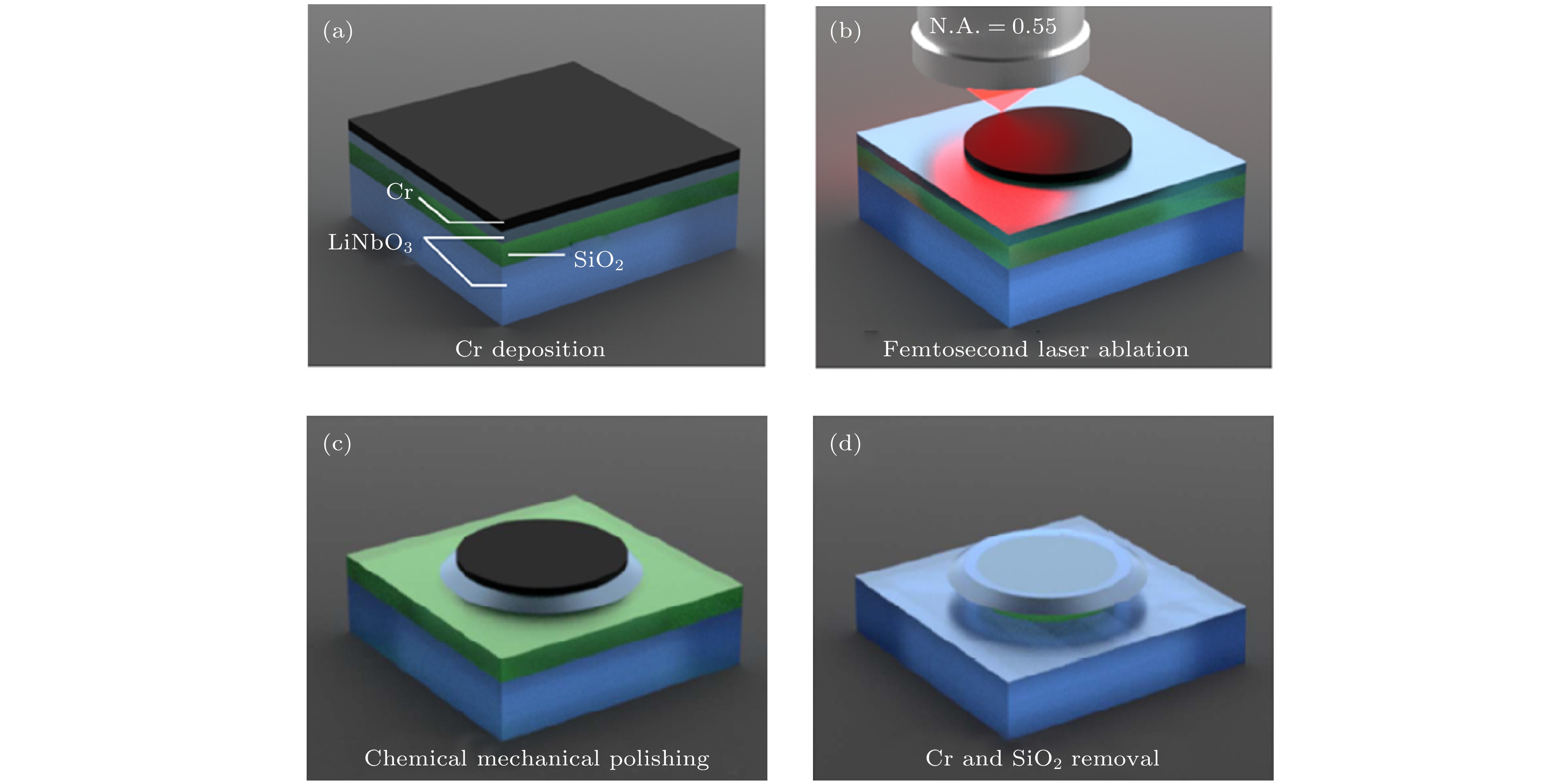
图 2 使用飞秒激光微加工制备LN片上微盘谐振腔的过程 (a) 在LN样品表面沉积Cr; (b) 飞秒激光加工将微盘图形转移到Cr膜上; (c) CMP过程将微盘图形转移到LN薄膜上; (d) 湿法刻蚀去除Cr膜和SiO2[20]
Fig. 2. Flow chart of fabricating LN microdisk using femtosecond laser micromachining: (a) Depositing metallic chromium on LN sample surface; (b) transferring microdisk graphics onto chrome layer by femtosecond laser micromachining; (c) transferring microdisk pattern onto LN film by CMP; (d) wet etching removes chromium film and SiO2[20].
图 3 PPLN薄膜片上脊形波导的制备流程 (a) 待加工的x切LN薄膜样品; (b) 沉积梳状金属极化电极; (c) 对金属电极施加极化电压; (d) 制作完成的PPLN脊形波导; (e) PPLN脊形波导俯视图, 深色部分为铁电畴反转区域; (f) 经过CMP或FIB技术处理之后的PPLN片上脊形波导侧壁[35]
Fig. 3. Preparation process of PPLN ridge waveguide: (a) The x-cut LN thin film sample to be processed; (b) deposition of comb-shaped metal polarized electrode; (c) application of polarization voltage to metal electrode; (d) the fabricated PPLN ridge waveguide; (e) top view of the PPLN ridge waveguide, the dark area is the domain inversion area; (f) PPLN ridge waveguide sidewall after CMP or FIB fabricating[35].
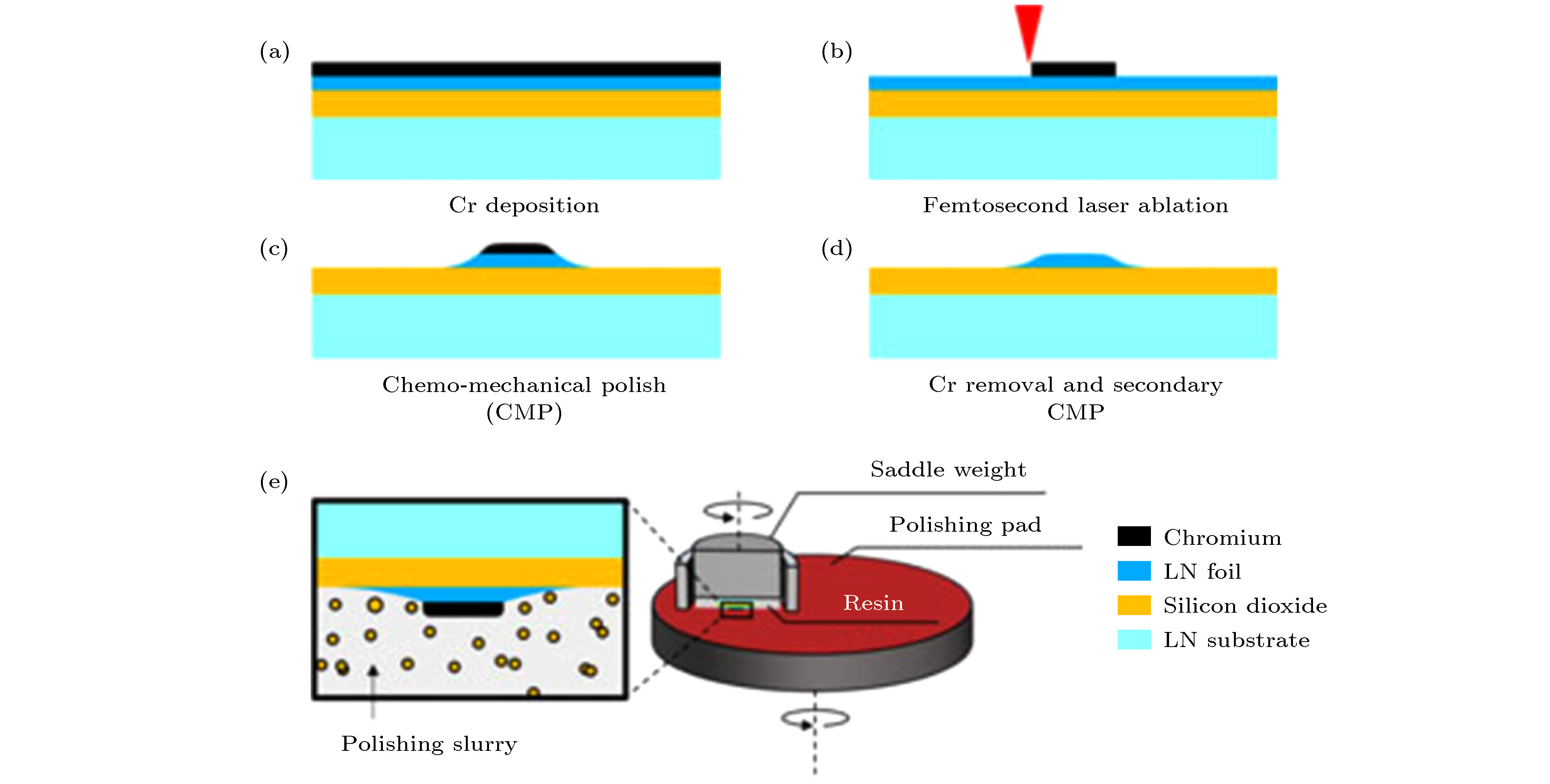
图 5 CMP技术制备LNOI片上光子学器件流程图 (a) 磁控溅射沉积Cr薄膜; (b) 飞秒激光微加工制备待加工图案; (c) CMP过程去除多余的LN; (d) 使用Cr腐蚀剂去除刻蚀掩模以及二次CMP过程; (e) CMP仪器示意图[38]
Fig. 5. Schematic of using CMP technology to prepare LNOI on-chip optics: (a) Depositing Cr film on LNOI by magnetron sputtering; (b) femtosecond laser processing defines the pattern to be processed; (c) CMP process to remove excess LN; (d) use Cr etchant to remove the etching mask and secondary CMP process; (e) schematic diagram of CMP instrument[38].
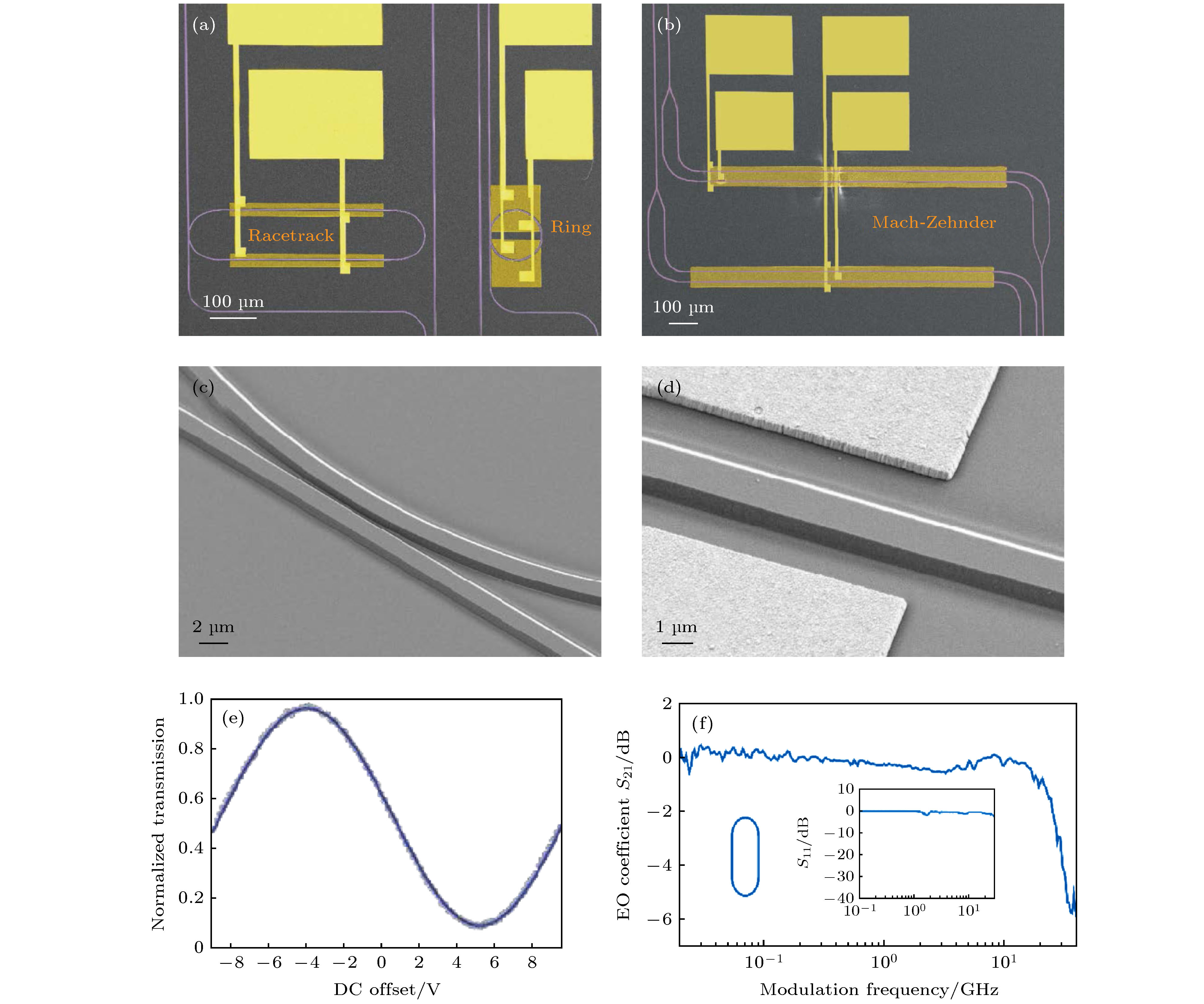
图 6 (a), (b) LNOI片上电光调制器的SEM图像; (c) 赛道型电光调制器耦合区域的放大图; (d) 电极与光波导的放大图; (e) M-Z型电光调制器的透射光谱; (f)赛道型电光调制器的电光调制带宽(9 V, 1480−1580 nm)[47]
Fig. 6. (a), (b) SEM images of the LNOI modulator; (c) enlarged view of the coupling area of the track modulator; (d) enlarged view of the electrode and optical waveguide; (e) transmission spectrum of MZI modulator; (f) electro-optical bandwidth of racetrack modulator (9 V, 1480−1580 nm)[47].
图 8 (a) 级联过程光谱, 其中抽运波长固定在1534.9 nm, 信号光波长分别位于1541.8 和1548.9 nm; (b) LN微盘中有效的FWM过程, FW闲频光功率依赖性和理论拟合, 信号光功率保持在5 mW[55]
Fig. 8. (a) Spectrum of the cascade process: the pump wavelength is fixed at 1534.9 nm, and the signal wavelength is at 1541.8 and 1548.9 nm. (b) Effective FWM process in LN microdisk, FW idler power dependence and theoretical fitting, the signal power is maintained at 5 mW[55].
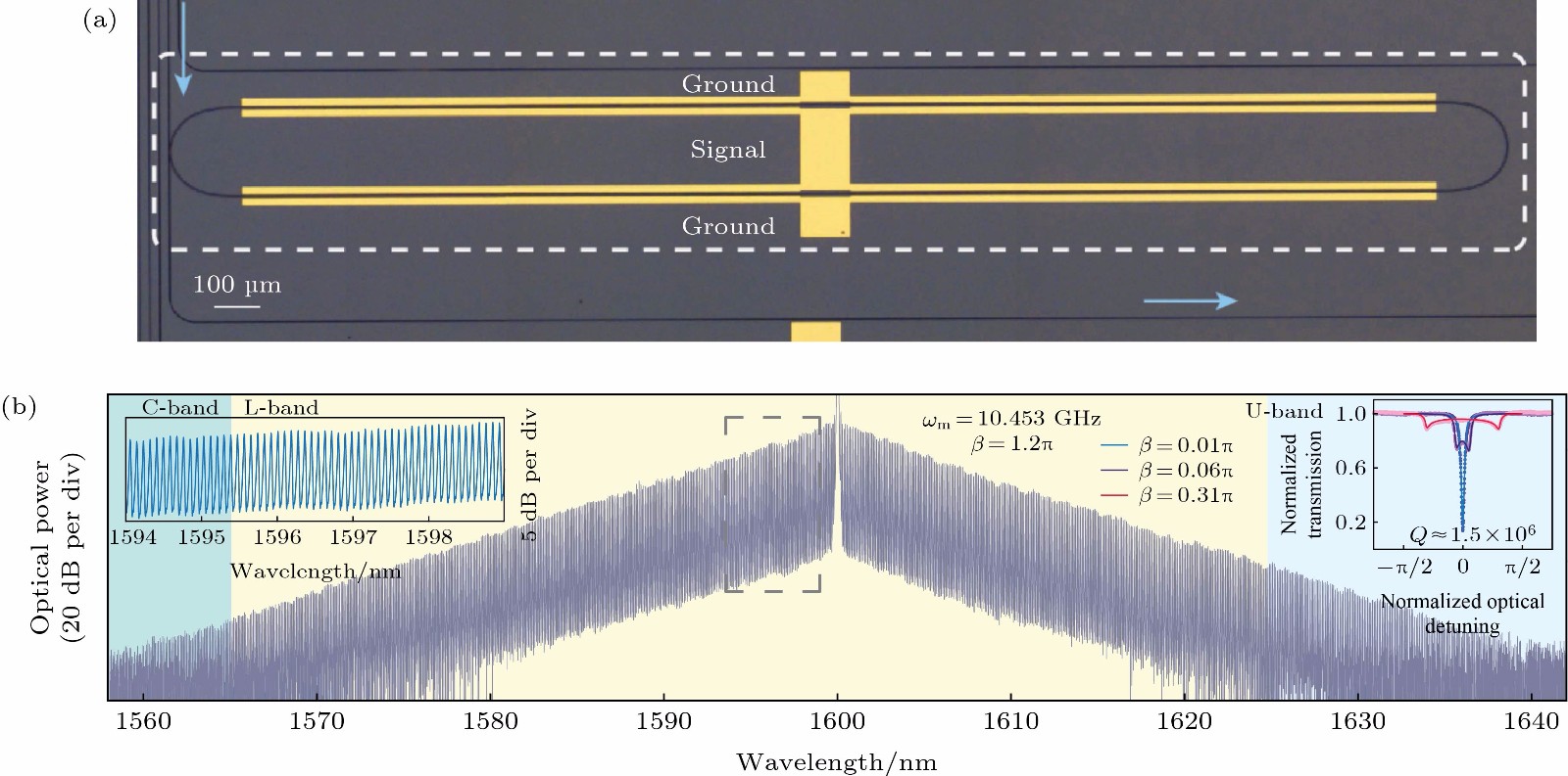
图 9 (a) LN微环谐振腔的显微照片, 黑线是蚀刻的光波导, 黄色区域是金电极; (b) 从微环谐振腔产生的EO频率梳的输出频谱, 左插图显示了几条梳齿的放大图, 梳齿之间的功率变化约为0.1 dB, 右插图显示了几个不同调制指数(β)的透射光谱[64]
Fig. 9. (a) Photograph of the LN microring resonator, the black line is an etched optical waveguide, and the yellow area is a gold electrode. (b) The output spectrum of the EO frequency comb generated from the micro-ring resonator. The left illustration shows an enlarged view of several comb teeth. The power variation between the comb teeth is about 0.1 dB. The right inset shows the transmission spectra of several different modulation indices (β)[64].
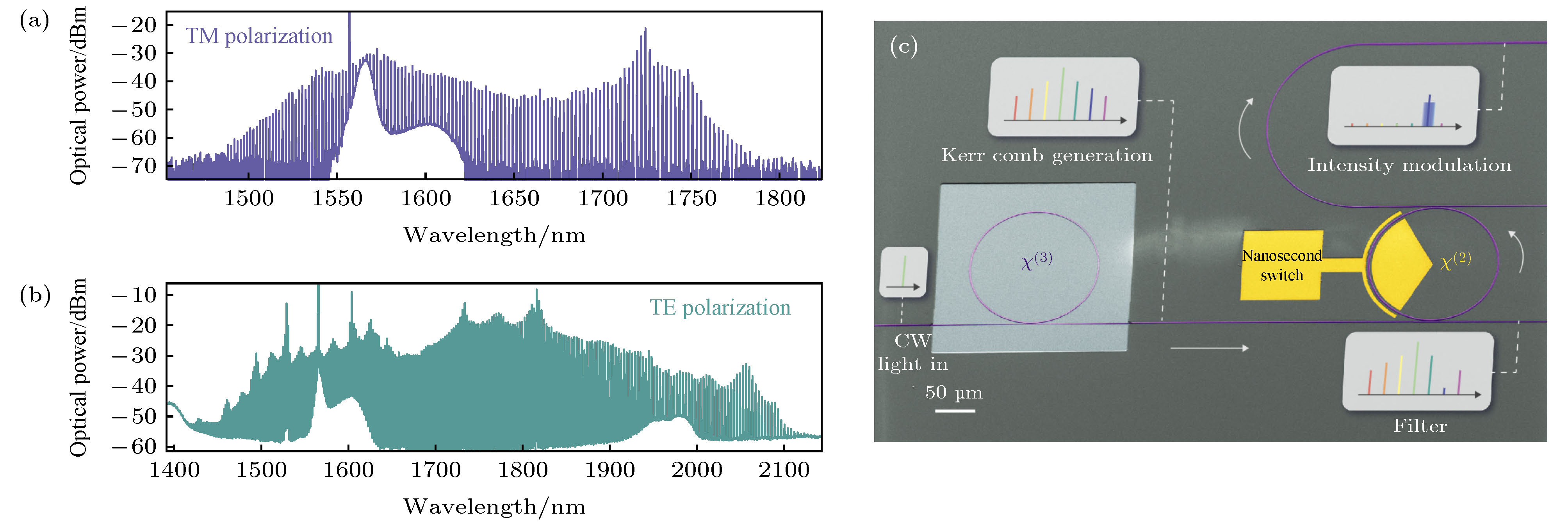
图 10 (a), (b)宽带频率梳的产生, 即当抽运功率为300 mW且输入信号与(a) TM模和(b) TE模共振时, 产生的频率梳频谱; (c) LN片上纳米光子学回路的SEM图像[65]
Fig. 10. (a), (b) Generation of a broadband frequency comb: The frequency comb spectrum is generated when the pump power is 300 mW and the input signal resonates with the (a) TM mode and the (b) TE mode; (c) SEM image of nanophotonic circuit on LN film[65].
表 1 不同加工手段制备的LN片上光子学器件的主要性能参数
Table 1. Main performance parameters of LN on-chip photonic devices fabricated by different fabrication techniques.
加工图案 微纳加工技术 尺寸 损耗(测量波长) 品质因子(测量波长/nm) 微盘[13] 紫外光刻技术 d = 50 μm — 1.5 × 10⁶ (1551.4) 微盘[12] r = 50 μm — 3.1 × 10⁵ (1550) 微盘[40] 电子束曝光技术 r = 25 μm — 2.9 × 10⁵ (1502) 微盘[41] r = 25 μm — 2.69 × 10⁵ (1548.78) 微环[1] r = 100 μm — 1.1 × 10⁷ (637) 微环[42] r = 80 μm — ~107 (1590) 光子晶体微腔[14] w = 750 nm — 1.09 × 10⁵ (1452) h = 250 nm a = 600 nm 微盘[21] 飞秒激光微加工 d = 29.92 μm — 9.61 × 10⁶ (1547.8) 微盘[20] d = 140 μm — 1.46 × 10⁷ (773.49) 双微盘[43] d = 29.92 μm — 1.35 × 10⁵ (1528.5) g = 138 nm 脊形波导[1] 电子束曝光技术 W = 480 nm 6 dB/m (635 nm) — H = 120 nm 脊形波导[42] W = 2.4 μm (2.7 ± 0.3) dB/m (1590 nm) — H = 0.25 μm 脊形波导[29] 异质集成 W = 1.3 μm 0.1 dB/m (1550 nm) — H = 0.5 μm 脊形波导[37] 化学机械抛光 W = 4 μm 4 dB/m (1550 nm) — H = 3 μm -
[1] Desiatov B, Shams A A, Zhang M, Wang C, Lončar M 2019 Optica 6 380
 Google Scholar
[2] He L Y, Zhang M, Shams A A, Zhu R R, Wang C, Lončar M 2019 Opt. Lett. 44 2314
 Google Scholar
[3] Nikogosyan D N 2005 Nonlinear Optical Crystals: A Complete Survey (New York: Springer Science + Business Media) pp35–53
[4] Poberaj G, Hu H, Sohler W, Günter P 2012 Laser Photonics Rev. 6 488
 Google Scholar
[5] Boes A, Corcoran B, Chang L, Bowers J, Mitchell A 2018 Laser Photonics Rev. 12 1700256
 Google Scholar
[6] Stepanenko O, Quillier E, Tronche H, Baldi P, Micheli M D 2014 IEEE Photonics Technol. Lett. 26 1557
 Google Scholar
[7] Bruel M 1995 Electron. Lett. 31 1201
 Google Scholar
[8] Ramadan A T, Levy M, Osgood J R M 2000 Appl. Phys. Lett. 76 1407
 Google Scholar
[9] Roth R M, Djukic D, Lee Y S, Jr R M O, Bakhru S, Laulicht B, Dunn K, Bakhru H, Wu L Q, Huang M B 2006 Appl. Phys. Lett. 89 112906
 Google Scholar
[10] Rabiei P, Gunter P 2004 Appl. Phys. Lett. 85 4603
 Google Scholar
[11] Djukic D, Cerda P G, Roth R M, Jr R M O, Bakhru S, Bakhru H 2007 Appl. Phys. Lett. 90 171116
 Google Scholar
[12] Wang J, Zhu B W, Hao Z Z, Bo F, Wang X L, Gao F, Li Y G, Zhang G Q, Xu J J 2016 Opt. Express 24 21869
 Google Scholar
[13] Wang L, Wang C, Wang J, Bo F, Zhang M, Gong Q H, Lončar M, Xiao Y F 2018 Opt. Lett. 43 2917
 Google Scholar
[14] Liang H X, Luo R, He Y, Jiang H W, Lin Q 2017 Optica 4 1251
 Google Scholar
[15] Wang M, Xu Y X, Fang Z W, Liao Y, Wang P, Chu W, Qiao L L, Lin J T, Fang W, Cheng Y 2017 Opt. Express 25 124
 Google Scholar
[16] Fang Z W, Lin J T, Wang M, Liu Z M, Yao J P, Qiao L L, Cheng Y 2015 Opt. Express 23 27941
 Google Scholar
[17] Song J X, Lin J T, Tang J L, Liao Y, He F, Wang Z H, Qiao L L, Sugioka K, Cheng Y 2014 Opt. Express 22 14792
 Google Scholar
[18] Jia Y C, Chen F 2019 Chin. Opt. Lett. 17 012302
 Google Scholar
[19] Chen F, Vázquez de Aldana J R 2014 Laser Photonics Rev. 8 251
 Google Scholar
[20] Wu R B, Zhang J H, Yao N, Fang W, Qiao L L, Fang C, Lin J T, Cheng Y 2018 Opt. Lett. 43 4116
 Google Scholar
[21] Zheng Y L, Fang Z W, Liu S J, Cheng Y, Chen X F 2019 Phys. Rev. Lett. 122 253902
 Google Scholar
[22] Fang Z W, Xu Y X, Wang M, Qiao L L, Lin J T, Fang W, Cheng Y 2017 Sci. Rep. 7 45610
 Google Scholar
[23] Rao A, Fathpour S 2018 IEEE J. Sel. Top. Quantum Electron. 24 8200912
 Google Scholar
[24] Rao A, Fathpour S 2018 IEEE J. Sel. Top. Quantum Electron. 24 3400114
 Google Scholar
[25] Honardoost A, Gonzalez G F C, Khan S, Malinowski M, Rao A, Tremblay J E, Yadav A, Richardson K, Wu M C, Fathpour S 2018 IEEE Photonics J. 10 4500909
 Google Scholar
[26] Gonzalez G F C, Malinowski M, Honardoost A, Fathpour S 2019 Appl. Opt. 58 D1
 Google Scholar
[27] Rao A, Abdelsalam K, Sjaardema T, Honardoost A, Camacho G G F, Fathpour S 2019 Opt. Express 27 25920
 Google Scholar
[28] Wang T, Ng D K T, Ng S K, Toh Y T, Chee A K L, Chen G F R, Wang Q, Tan D T H 2015 Laser Photonics Rev. 9 498
 Google Scholar
[29] Honardoost A, Juneghani F A, Safian R, Fathpour S 2019 Opt. Express 27 6495
 Google Scholar
[30] Rao A, Chiles J, Khan S, Toroghi S, Malinowski M, Camacho G G F, Fathpour S 2017 Appl. Phys. Lett. 110 111109
 Google Scholar
[31] Rao A, Patil A, Chiles J, Malinowski M, Novak S, Richardson K, Rabiei P, Fathpour S 2015 Opt. Express 23 22746
 Google Scholar
[32] Luo R, He Y, Liang H X, Li M X, Lin Q 2018 Optica 5 1006
 Google Scholar
[33] He Y, Liang H X, Luo R, Li M X, Lin Q 2018 Opt. Express 26 16315
 Google Scholar
[34] Chen J Y, Sua Y M, Fan H, Huang Y P 2018 OSA Continuum 1 229
 Google Scholar
[35] Chen J Y, Sua Y M, Ma Z H, Tang C, Li Z, Huang Y P 2019 OSA Continuum 2 2914
 Google Scholar
[36] Reich M, Korte F, Fallnich C, Welling H, Tünnermann A 1998 Opt. Lett. 23 1817
 Google Scholar
[37] Wolf R, Breunig I, Zappe H, Buse K 2018 Opt. Express 26 19815
 Google Scholar
[38] Wang M, Wu R B, Lin J T, Zhang J H, Fang Z W, Chai Z F, Cheng Y 2019 Quantum Eng. 1 1
 Google Scholar
[39] Fang Z W, Haque S, Lin J T, Wu R B, Zhang J H, Wang M, Zhou J X, Rafa M, Tao L, Cheng Y 2019 Opt. Lett. 44 1214
 Google Scholar
[40] Luo R, Jiang H W, Liang H X, Chen Y P, Lin Q 2017 Opt. Lett. 42 1281
 Google Scholar
[41] Jiang H W, Luo R, Liang H X, Chen X F, Chen Y P, Lin Q 2017 Opt. Lett. 42 3267
 Google Scholar
[42] Zhang M, Wang C, Cheng R, Shams A A, Lončar M 2017 Optica 4 1536
 Google Scholar
[43] Fang Z W, Yao N, Wang M, Lin J T, Zhang J H, Wu R B, Qiao L L, Fang W, Lu T, Cheng Y 2017 Int. J. Optomechatronics 11 47
 Google Scholar
[44] Guarino A, Poberaj G, Rezzonico D, Riccardo D, Günter P 2007 Nat. Photonics 1 407
 Google Scholar
[45] Ren T, Zhang M, Wang C, Shao L B, Reimer C, Zhang Y, King O, Esman R, Cullen T, Lončar M 2019 IEEE Photonics Technol. Lett. 31 889
 Google Scholar
[46] Jin M W, Chen J Y, Sua Y M, Huang Y P 2019 Opt. Lett. 44 1265
 Google Scholar
[47] Wang C, Zhang M, Stern B, Lipson M, Lončar M 2018 Opt. Express 26 1547
 Google Scholar
[48] Wang C, Zhang M, Chen X, Bertrand M, Shams A A, Chandrasekhar S, Winzer P, Lončar M 2018 Nature 562 101
 Google Scholar
[49] He M B, Xu M Y, Ren Y X, Jian J, Ruan Z L, Xu Y S, Gao S Q, Sun S H, Wen X Q, Zhou L D, Liu L, Guo C J, Chen H, Yu S Y, Liu L, Cai X L 2019 Nat. Photonics 13 359
 Google Scholar
[50] Ahmed A N R, Nelan S, Shi S Y, Yao P, Mercante A, Prather D W 2020 Opt. Lett. 45 1112
 Google Scholar
[51] Thomaschewski M, Zenin V A, Wolff C, Bozhevolnyi S I 2020 Nat. Commun. 11 748
 Google Scholar
[52] Luo R, He Y, Liang H X, Li M X, Ling J W, Lin Q 2019 Phys. Rev. Appl. 11 034026
 Google Scholar
[53] Luo R, Jiang H W, Rogers S, Liang H X, He Y, Lin Q 2017 Opt. Express 25 24531
 Google Scholar
[54] Lin J T, Yao N, Hao Z Z, Zhang J h, Mao W B, Wang M, Chu W, Wu R B, Fang Z W, Qiao L L, Fang W, Bo F, Cheng Y 2019 Phys. Rev. Lett. 122 173903
 Google Scholar
[55] Liu S J, Zheng Y L, Fang Z W, Ye X N, Cheng Y, Chen X F 2019 Opt. Lett. 44 1456
 Google Scholar
[56] Ye X N, Liu S J, Chen Y P, Zheng Y L, Chen X F 2020 Opt. Lett. 45 523
 Google Scholar
[57] Wolf R, Jia Y C, Bonaus S, Werner C S, Herr S J, Breunig I, Buse K, Zappe H 2018 Optica 5 872
 Google Scholar
[58] Chen J Y, Ma Z H, Sua Y M, Li Z, Tang C, Huang Y P 2019 Optica 6 1244
 Google Scholar
[59] Lu J J, Surya J B, Liu X W, Bruch A W, Gong Z, Xu Y T, Tang H X 2019 Optica 6 1455
 Google Scholar
[60] Hao Z Z, Zhang L, Gao A, Mao W B, Lyu X D, Gao X M, Bo F, Gao F, Zhang G Q, Xu J J 2018 Sci. China, Ser. G 61 114211
 Google Scholar
[61] Hao Z Z, Zhang L, Mao W B, Gao A, Gao X M, Gao F, Bo F, Zhang G Q, Xu J J 2020 Photonics Res. 8 311
 Google Scholar
[62] Sua Y M, Chen J Y, Huang Y P 2018 Opt. Lett. 43 2965
 Google Scholar
[63] Niu Y F, Lin C, Liu X Y, Chen Y, Hu X P, Zhang Y, Cai X L, Gong Y X, Xie Z D, Zhu S N 2020 Appl. Phys. Lett. 116
 Google Scholar
[64] Zhang M, Buscaino B, Wang C, Shams A A, Reimer C, Zhu R R, Kahn J M, Lončar M 2019 Nature 568 373
 Google Scholar
[65] Wang C, Zhang M, Yu M J, Zhu R R, Hu H, Lončar M 2019 Nat. Commun. 10 1
 Google Scholar
[66] Yu M J, Desiatov B, Okawachi Y, Gaeta A L, Lončar M 2019 Opt. Lett. 44 1222
 Google Scholar
[67] Jiang W C, Lin Q 2016 Sci. Rep. 6 36920
 Google Scholar
[68] Cai L T, Mahmoud A, Khan M, Mahmoud M, Mukherjee T, Bain J, Piazza G 2019 Photonics Res. 7 1003
 Google Scholar
[69] Yao N, Zhou J X, Gao R H, Lin J T, Wang M, Cheng Y, Fang W, Tong L M 2020 Opt. Express 28 12416
 Google Scholar
[70] [71] Chen Z H, Peng R H, Wang Y w, Zhu H B, Hu H 2017 Opt. Mater. Express 7 4010
 Google Scholar
[72] Krasnokutska I, Chapman R J, Tambasco J L J, Peruzzo A 2019 Opt. Express 27 17681
 Google Scholar
[73] Khan M, Bain J A, Piazza G 2019 Opt. Lett. 44 4558
 Google Scholar
计量
- 文章访问数: 26925
- PDF下载量: 1103
- 被引次数: 0


 下载:
下载:
