-
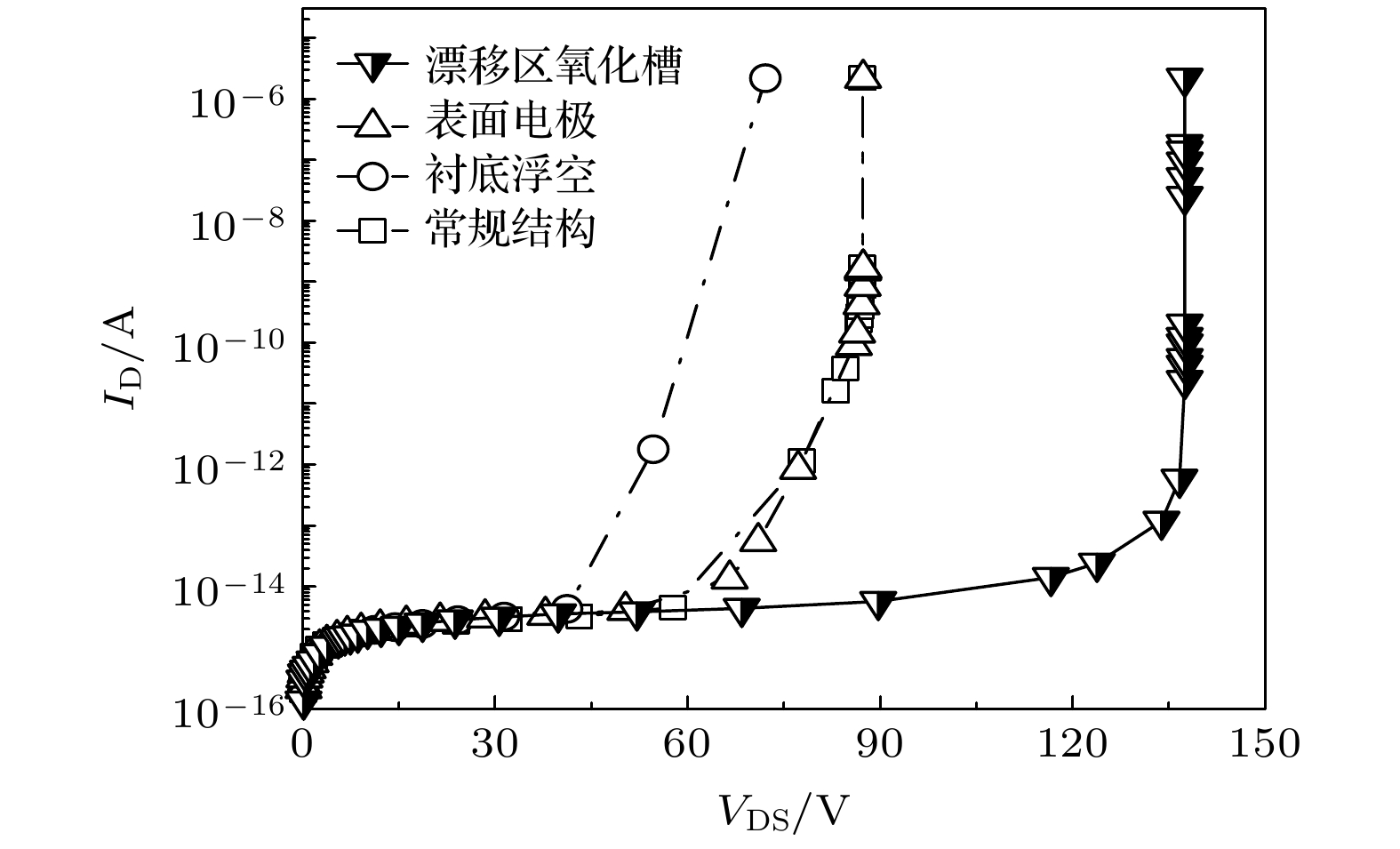
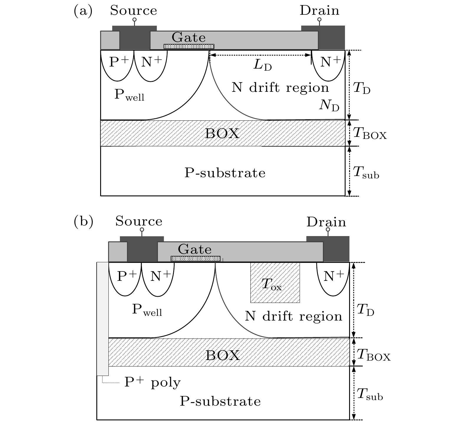
针对有机半导体领域的发展要求, 报道了一种能够应用于有机半导体领域衬底浮空的新型SOI LDMOS (silicon on insulator lateral double-diffused metal oxide semiconductor)功率器件, 不同于传统无机半导体中SOI LDMOS功率器件, 该新型器件可以与绝缘的柔性衬底结合应用于有机半导体领域, 这给有机半导体领域的研究方向提供了新的可能. 本文通过仿真和流片实验共同验证了当常规SOI LDMOS缺失衬底电极后, 比导通电阻和阈值电压均无明显变化, 但击穿电压会因为缺失衬底电极和纵向电场而下降15%左右. 针对该现象提出了一个具有表面衬底电极和漂移区氧化槽的新型SOI LDMOS功率器件, 该新型器件能够重新给衬底提供电极、优化横纵向电场、不明显改变比导通电阻与阈值电压, 同时将常规SOI LDMOS的击穿电压提高57.54%, 缓解了应用于有机半导体领域带来的不良影响. 为传统功率半导体应用于有机半导体领域的研究提供了可能, 对于有机半导体研究领域的拓展具有创新意义.With the rapid development of the traditional inorganic semiconductor industry, the improvement of its electrical performance is gradually approaching to the limit. It is difficult to continue to improve the performance, lessen the size, and reduce the cost. Therefore, organic semiconductor materials and devices with simple process and low cost have been found and gradually become a new research hotspot. Although organic semiconductor materials and devices are developing rapidly, their electrical properties, such as carrier mobility, are considerably inferior to those of inorganic semiconductors, and their research direction and application prospect are relatively fixed and single. They are developed only in display, sensing, photoelectric conversion and other fields, but the researches on switching power devices, integrated circuits and other fields are still relatively blank. At the same time, power devices are used only in the field of inorganic semiconductors. Therefore, in order to expand the research direction of organic semiconductors and power devices at the same time, a novelsilicon on insulator lateral double-diffused metal oxide semiconductor (SOI LDMOS)power device is reported in this paper. Unlike the SOI LDMOS power devices in traditional inorganic semiconductors, this novel device can be used in the field of organic semiconductors by combining with insulated flexible substrates, which provides a new possibility for the research direction of organic semiconductors. In this paper, both simulation and experiment verify that specific on-resistance (RON,sp) and threshold voltage (VTH) do not change significantly when the conventional SOI LDMOS lacks the substrate electrode, but the breakdown voltage decreases by about 15% due to the absence of the substrate electrode or the longitudinal electric field. In response to this phenomenon, in this paper proposed is a novel SOI LDMOS power device that possesses surface substrate electrodes and drift zone oxide trenches. This novel device can provide electrodes for the substrate again, optimize the horizontal and vertical electric field, and significantly change neither of the RON,sp and the VTH. At the same time, the breakdown voltage (BV) of conventional SOI LDMOS is increased by 57.54%, which alleviates the adverse effects caused by the application in the field of organic semiconductors. This novel SOI LDMOS power device provides the possibility of applying traditional power semiconductors to the research of organic semiconductors, and has innovative significance for expanding the organic semiconductor research.
-
Keywords:
- silicon on insulator /
- substrate electrodes /
- breakdown voltage /
- oxidation groove
[1] 李琦, 李肇基, 张波 2007 物理学报 56 6660
 Google Scholar
Li Q, Li Z J, Zhang B 2007 Acta Phys. Sin. 56 6660
 Google Scholar
[2] Lei J M, Hu S D, Wang S, Lin Z 2017 International Conference on Electron Devices and Solid-State Circuits (EDSSC) Hsinchu, China, October 18−20, 2017 p1
[3] Okawa T, Eguchi H, Taki M, Hamada K 2016 28th International Symposium on Power Semiconductor Devices and ICs (ISPSD) Prague, Czech Republic, June 12−16, 2016 p435
[4] Cheng J J, Wu S Y, Chen W Z, Huang H M, Yi B 2019 IEEE J. Electron Devices Soc. 7 682
 Google Scholar
[5] Xia C, Cheng X H, Wang Z J, Xu D W, Cao D, Zheng L, Shen L Y, Yu Y H, Shen D S 2014 IEEE Trans. Electron Devices 61 3477
 Google Scholar
[6] Fang Z Q, Xu Z Z, Qian W S 2019 China Semiconductor Technology International Conference (CSTIC) Shanghai, China, March 18−19, 2019 p1
[7] Tang P P, Wang Y, Bao M T, Luo X, Cao F, Yu C H 2019 Micro & Nano Letters 14 420
[8] Dong Z M, Duan B X, Fu C, Guo H J, Cao Z, Yang Y T 2018 IEEE Electron Device Lett. 39 1358
 Google Scholar
[9] Wang Y D, Duan B X, Song H T, Yang Y T 2020 IEEE Electron Device Lett. 41 1681
 Google Scholar
[10] Duan B X, Cao Z, Yuan X N, Yuan S, Yang Y T 2015 IEEE Electron Device Lett. 36 47
 Google Scholar
[11] Xu Q, Guo Y F, Zhang Y, Liu L L, Yao J F, Sheu G 2012 Procedia Eng. 29 668
 Google Scholar
[12] 段宝兴, 曹震, 袁小宁, 杨银堂 2014 物理学报 63 227302
 Google Scholar
Duan B X, Cao Z, Yuan X N, Yang Y T 2014 Acta Phys. Sin. 63 227302
 Google Scholar
[13] Zhang B, Cheng J B, Qiao M, Li Z J 2008 9th International Conference on Solid-State and Integrated-Circuit Technology Beijing, China, October 20−23, 2008 p164
[14] Cao Z, Duan B X, Shi T T, Dong Z M, Guo H J, Yang Y T 2018 IEEE Trans. Electron Devices 65 2565
 Google Scholar
[15] Cao Z, Duan B X, Yuan S, Guo H J, Lv J M, Shi T T, Yang Y T 2017 29th International Symposium on Power Semiconductor Devices and IC's (ISPSD) Sapporo, Japan, May 28–June 1, 2017 p283
[16] Cao Z, Duan B X, Shi T T, Yuan S, Yang Y T 2018 IETE Tech. Rev. 35 402
 Google Scholar
[17] 段宝兴, 李春来, 马剑冲, 袁嵩, 杨银堂 2015 物理学报 64 067304
 Google Scholar
Duan B X, Li C L, Ma J C, Yuan S, Yang Y T 2015 Acta Phys. Sin. 64 067304
 Google Scholar
[18] Wu L J, Zhang W T, Shi Q, Cai P F, He H C 2014 Electron. Lett. 50 1982
 Google Scholar
[19] Duan B X, Li M Z, Dong Z M, Wang Y D, Yang Y T 2019 IEEE Trans. Electron Devices 66 4836
 Google Scholar
[20] Wu L J, Wu Y Q, Lei B, Zhang Y Y, Huang Y, Zhu L 2019 Micro & Nano Letters 14 600
 Google Scholar
[21] Cao Z, Duan B X, Song H T, Xie F Y, Yang Y T 2019 IEEE Trans. Electron Devices 66 2327
 Google Scholar
[22] Tsai C C 2011 16th Opto-Electronics and Communications Conference Kaohsiung, China, July 4−8, 2011 p370
[23] Zhang J 2018 International Flexible Electronics Technology Conference (IFETC) Ottawa, Canada, August 7−9, 2018 p1
[24] Kadija I 2019 22nd European Microelectronics and Packaging Conference & Exhibition (EMPC) Pisa, Italy, September 16−19 2019 p1
[25] Guo S N, Cheng J J, Chen X B 2019 IEEE 13th International Conference on Power Electronics and Drive Systems (PEDS) Toulouse, France, July 9−12, 2019 p1
[26] Cao Z, Jiao L C 2020 IEEE J. Electron Devices Soci. 8 890
 Google Scholar
-
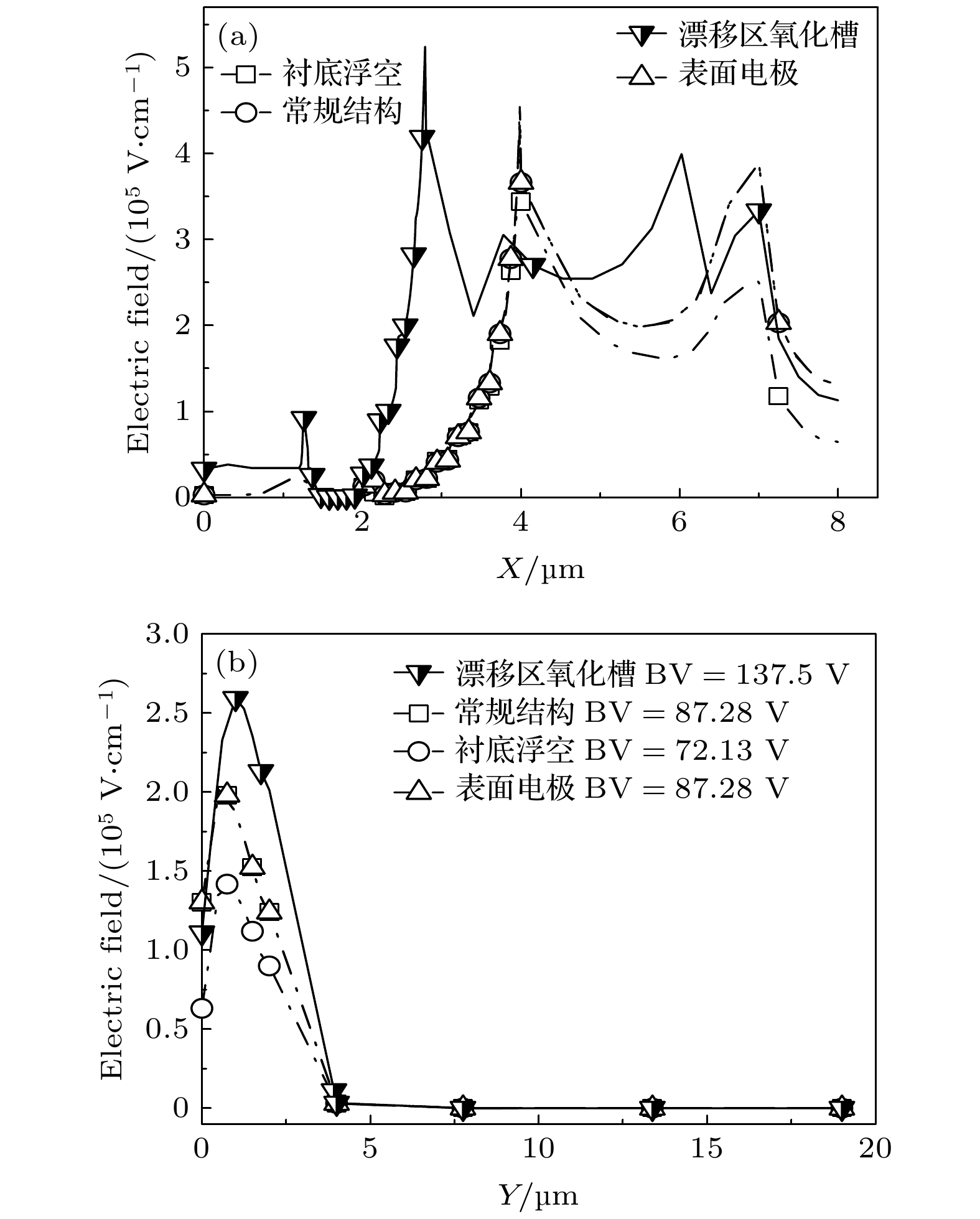
图 3 衬底厚度Tsub = 15 μm, 漂移区长度LD = 4 μm的SOI LDMOS电场分布图 (a) 表面电场分布图; (b) 纵向电场分布图
Fig. 3. Electric field distribution graph for SOI LDMOS with substrate thickness of 15 μm (Tsub = 15 μm) and drift zone length of 4 μm (LD = 4 μm): (a) Surface electric field distribution graph; (b) longitudinal electric field distribution graph.
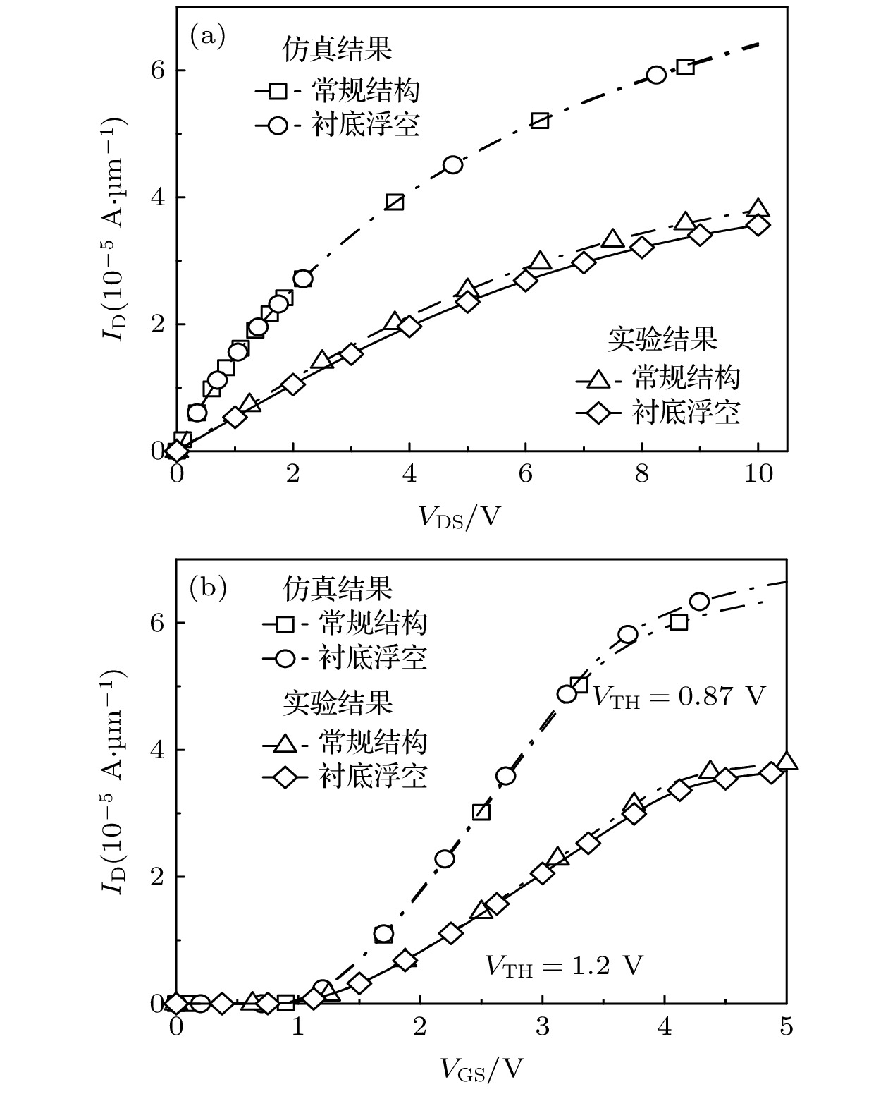
图 4 衬底厚度Tsub = 15 μm, 漂移区长度LD = 4 μm的SOI LDMOS仿真和实验结果对比 (a) VGS = 5 V时的输出特性曲线; (b) VDS = 10 V时的转移特性曲线
Fig. 4. Comparison of simulation and experimental results for SOI LDMOS with substrate thickness of 15 μm (Tsub = 15 μm) and drift zone length of 4 μm (LD = 4 μm): (a) Output characteristic curve when VGS = 5 V; (b) transfer characteristic curve when VDS = 10 V.
表 1 常规SOI LDMOS与衬底浮空SOI LDMOS器件仿真最优参数
Table 1. Simulation optimal parameters of conventional SOI LDMOS/ substrate floating SOI LDMOS devices.
器件最优参数(仿真) 常规SOI LDMOS/衬底
浮空SOI LDMOS漂移区厚度Td/μm 2 埋氧层厚度TOX/μm 2 衬底厚度Tsub/μm 15 漂移区N型掺杂浓度, Nd/cm–3 1.5 × 10¹⁶ 衬底P型掺杂浓度Psub/cm–3 2 × 10¹⁴ 阱区P型掺杂浓度Pwell/cm–3 1.5 × 10¹⁶ 表 2 新型SOI LDMOS器件仿真最优参数
Table 2. Simulation optimal parameters for novel SOI LDMOS devices.
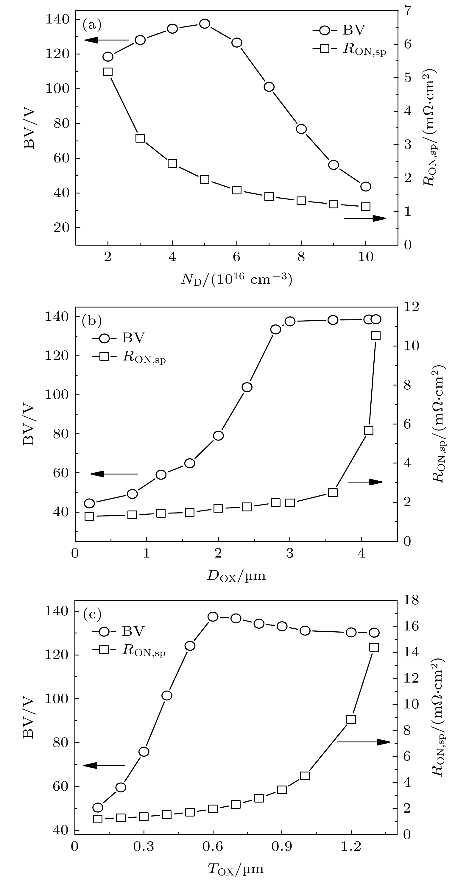
器件最优参数(仿真) 新型SOI LDMOS 漂移区厚度TD/μm 2 埋氧层厚度TOX/μm 2 衬底厚度Tsub/μm 15 氧化槽宽度WT/μm 3 氧化槽深度DT/μm 0.6 漂移区N型掺杂浓度ND/(1014 cm–3) 5 衬底P型掺杂浓度Psub/(1014 cm–3) 4 阱区P型掺杂浓度Pwell/(1016 cm–3) 6 -
[1] 李琦, 李肇基, 张波 2007 物理学报 56 6660
 Google Scholar
Li Q, Li Z J, Zhang B 2007 Acta Phys. Sin. 56 6660
 Google Scholar
[2] Lei J M, Hu S D, Wang S, Lin Z 2017 International Conference on Electron Devices and Solid-State Circuits (EDSSC) Hsinchu, China, October 18−20, 2017 p1
[3] Okawa T, Eguchi H, Taki M, Hamada K 2016 28th International Symposium on Power Semiconductor Devices and ICs (ISPSD) Prague, Czech Republic, June 12−16, 2016 p435
[4] Cheng J J, Wu S Y, Chen W Z, Huang H M, Yi B 2019 IEEE J. Electron Devices Soc. 7 682
 Google Scholar
[5] Xia C, Cheng X H, Wang Z J, Xu D W, Cao D, Zheng L, Shen L Y, Yu Y H, Shen D S 2014 IEEE Trans. Electron Devices 61 3477
 Google Scholar
[6] Fang Z Q, Xu Z Z, Qian W S 2019 China Semiconductor Technology International Conference (CSTIC) Shanghai, China, March 18−19, 2019 p1
[7] Tang P P, Wang Y, Bao M T, Luo X, Cao F, Yu C H 2019 Micro & Nano Letters 14 420
[8] Dong Z M, Duan B X, Fu C, Guo H J, Cao Z, Yang Y T 2018 IEEE Electron Device Lett. 39 1358
 Google Scholar
[9] Wang Y D, Duan B X, Song H T, Yang Y T 2020 IEEE Electron Device Lett. 41 1681
 Google Scholar
[10] Duan B X, Cao Z, Yuan X N, Yuan S, Yang Y T 2015 IEEE Electron Device Lett. 36 47
 Google Scholar
[11] Xu Q, Guo Y F, Zhang Y, Liu L L, Yao J F, Sheu G 2012 Procedia Eng. 29 668
 Google Scholar
[12] 段宝兴, 曹震, 袁小宁, 杨银堂 2014 物理学报 63 227302
 Google Scholar
Duan B X, Cao Z, Yuan X N, Yang Y T 2014 Acta Phys. Sin. 63 227302
 Google Scholar
[13] Zhang B, Cheng J B, Qiao M, Li Z J 2008 9th International Conference on Solid-State and Integrated-Circuit Technology Beijing, China, October 20−23, 2008 p164
[14] Cao Z, Duan B X, Shi T T, Dong Z M, Guo H J, Yang Y T 2018 IEEE Trans. Electron Devices 65 2565
 Google Scholar
[15] Cao Z, Duan B X, Yuan S, Guo H J, Lv J M, Shi T T, Yang Y T 2017 29th International Symposium on Power Semiconductor Devices and IC's (ISPSD) Sapporo, Japan, May 28–June 1, 2017 p283
[16] Cao Z, Duan B X, Shi T T, Yuan S, Yang Y T 2018 IETE Tech. Rev. 35 402
 Google Scholar
[17] 段宝兴, 李春来, 马剑冲, 袁嵩, 杨银堂 2015 物理学报 64 067304
 Google Scholar
Duan B X, Li C L, Ma J C, Yuan S, Yang Y T 2015 Acta Phys. Sin. 64 067304
 Google Scholar
[18] Wu L J, Zhang W T, Shi Q, Cai P F, He H C 2014 Electron. Lett. 50 1982
 Google Scholar
[19] Duan B X, Li M Z, Dong Z M, Wang Y D, Yang Y T 2019 IEEE Trans. Electron Devices 66 4836
 Google Scholar
[20] Wu L J, Wu Y Q, Lei B, Zhang Y Y, Huang Y, Zhu L 2019 Micro & Nano Letters 14 600
 Google Scholar
[21] Cao Z, Duan B X, Song H T, Xie F Y, Yang Y T 2019 IEEE Trans. Electron Devices 66 2327
 Google Scholar
[22] Tsai C C 2011 16th Opto-Electronics and Communications Conference Kaohsiung, China, July 4−8, 2011 p370
[23] Zhang J 2018 International Flexible Electronics Technology Conference (IFETC) Ottawa, Canada, August 7−9, 2018 p1
[24] Kadija I 2019 22nd European Microelectronics and Packaging Conference & Exhibition (EMPC) Pisa, Italy, September 16−19 2019 p1
[25] Guo S N, Cheng J J, Chen X B 2019 IEEE 13th International Conference on Power Electronics and Drive Systems (PEDS) Toulouse, France, July 9−12, 2019 p1
[26] Cao Z, Jiao L C 2020 IEEE J. Electron Devices Soci. 8 890
 Google Scholar
计量
- 文章访问数: 7471
- PDF下载量: 90
- 被引次数: 0


 下载:
下载:
