


-
光波单向传输器件在全光计算和信息处理方面具有重要应用. 本文提出一种具有完全光子带隙的硅基空气孔光子晶体漏斗型光波导结构, 在光通信波段可实现单向传输特性. 漏斗型光波导可打破光波对称传输, 引入点缺陷通过模式转换与失配进一步抑制反向透射, 并研究了不同的点缺陷类型与位置对反向透射的影响. 采用时域有限差分法进行数值计算, 优化选取了最佳的点缺陷模式. 结果显示, 单柱型点缺陷在向左移动5a (a为光子晶体晶格常数, a = 470 nm)时, 横电(TE)偏振光在工作波长1550 nm处正向透射率为0.716, 透射对比度为0.929, 工作带宽为111 nm. 另外, 本文提出的光波单向传输器件结构简单、工艺要求低, 有望为集成光路中单向传输器件设计提供新的解决方案.It will be a future trend to apply quantum photonic technology to communication technology and information processing. One of major developing directions of quantum photonic technology is the miniaturization and on-chip integration. Like the diodes in integrated electric circuitry, optical unidirectional transmitter devices (UTDs) play an important role in processing the quantum information and also represent the main components of integrated optical devices. Thus, the design of UTDs has become one of the research hotspots. With photonic bandgap and localization characteristics, as well as easy micro-nano scaled integration, the photonic crystals (PCs) are often preferred when used to develop micro-nano integrated optical devices. At present, the common methods of achieving UTD with photonic crystals include directional bandgap mismatch, asymmetrical coupling by a micro-cavity, odd-even mode conversion, total reflection of photonic crystals with grating and photonic crystal heterostructure, etc. However, these optical unidirectional transmitters gained through the above methods generally have a low forward transmission, narrow working band, complex structure, etc. In the paper a novel method of UTD is put forward based on photonic crystal and a UTD of funnel-shaped waveguide is designed. The design of the device is divided into two parts: optimal funnel waveguide design and optimal point defect design. The band structure of TE polarized photonic crystal is calculated by R-soft. A triangular lattice circular air hole photonic crystal with complete photonic band gap is used as the initial structure and line defects are introduced to form a funnel-shaped waveguide structure (FSWS). The FSWS consists of the first waveguide W1, the second waveguide W2 and a funnel cavity. The funnel cavity is shaped like a funnel and located at the coupling between W1 and W2. Owing to the unique characteristics of the waveguide, the light wave transmission will be localized in the waveguide, which is conducive to improving the forward transmission. The influence of width variation of W2 with forward and backward incident light are analyzed by the finite difference time domain (FDTD) method, and W2 is selected as a waveguide formed by removing 11 rows of air holes. The FSWS achieves the initial asymmetric transmission, while the backward transmission remains high. Further studies are conducted to introduce four types of point defects to suppress the backward transmittance. The point defects refer to moving one or two air holes. In the work the FDTD is also used to calculate four kinds of point defect backward transmittance spectra and optimize the positions of point defects. Finally, it is found that when the optimal point defect mode is type I and d = 5a, the forward transmission (Tf) and transmission contrast (C ) at 1550 nm are 0.716 and 0.929, respectively. Working bandwidth (B) can be increased up to 111 nm (1501–1612 nm). By mode analysis, it is found that the point defect introduces mode mismatch between W1 and W2, by converting the fundamental mode in W2 into high-order modes. Thus, the back-propagating light waves in W2 cannot effectively couple into W1, resulting in complete blockage of backward propagation. In addition, the structure is made of silicon based air hole photonic crystal. The 2D air-hole PC slab is mature and even compatible with conventional complementary metal oxide semiconductor (CMOS) processing. The designed UTD is easy to implement, and has the advantages of simplicity and high unidirectional transmission characteristics. Therefore, it can provide a new solution for UTDs with higher requirements for integrated optical path at present.
-
Keywords:
- funnel waveguide /
- complete photonic bandgap /
- point defect /
- unidirectional transmission /
- mode analysis
[1] Li M 2012 Sci. China Phys. Mech. 55 2316
 Google Scholar
[2] Lars T, Qiu M, Srinivasan A 2004 Chem. Phys. Chem. 5 1268
Google Scholar
[3] 武敏, 费宏明, 林瀚, 赵晓丹, 杨毅彪, 陈智辉 2021 物理学报 70 028501
Google Scholar
Wu M, Fei H M, Lin H, Zhao X D, Yang Y B, Chen Z H 2021 Acta Phys. Sin. 70 028501
Google Scholar
[4] Bulgakov E N, Sadreev A F 2014 Opt. Lett. 39 1787
Google Scholar
[5] Soltani A, Ouerghi F, AbdelMalek F 2017 Opt. Commun. 392 147
Google Scholar
[6] Li J, Ye H, Yu Z Y, Liu Y M 2017 Opt. Express 25 19129
Google Scholar
[7] Liu D Y, Yao L F, Zhai X M, Li M H, Dong J F 2014 Appl. Phys. A 116 9
Google Scholar
[8] Ahmet O, Hasan K, Hamza K 2018 J. Opt. Soc. Am. B 35 2111
[9] Ahmet O, Nazmi Y, Hasan K, Hamza K 2019 J. Opt. 21 055104
Google Scholar
[10] Li S, Huang L R, Ling Y H, Liu W B, Ba C F, Li H H 2019 Sci. Rep. 9 17117
Google Scholar
[11] Liu H, Zhang Y Z, Chen C, Bai B B, Zhang X, Zhang H C, Shao Q Y, Wu B, Zhao B L 2021 Opt. Laser Technol. 140 107033
Google Scholar
[12] Hadi R, Mohammad S, Yousef S K 2018 J. Opt. Commun. 39 375
Google Scholar
[13] Wang C, Zhou C Z, Li Z Y 2011 Opt. Express 19 26948
Google Scholar
[14] 刘丹, 胡森 2019 物理学报 024206
Google Scholar
Liu D, Hu S 2019 Acta Phys. Sin. 024206
Google Scholar
[15] Xie J Y, Hu X Y, Wang F F, Ao Y T, Gao W, Yang H, Gong Q H 2018 J. Opt. 20 034004
Google Scholar
[16] Liu B, Liu Y F, Li S J, He X D 2016 Opt. Commun. 368 7
Google Scholar
[17] Liu B, Liu Y F, Jia C, He X D 2016 Aip. Adv. 6 065316
Google Scholar
[18] Ye H, Zhang J Q N, Yu Z Y, Wang D L, Chen Z H 2015 Chin. Phys. B 24 094214
Google Scholar
[19] Ye H, Wang D L, Yu Z Y, Zhang J Q N, Chen Z H 2015 Opt. Express 23 9673
Google Scholar
[20] Chen J J, Huo S Y 2017 Opt. Mater. Express 7 1716
Google Scholar
[21] Fei H M, Zhang Q, Wu M, Lin H, Liu X, Yang Y B, Zhang M D, Guo R, Han X T 2020 Appl. Optics 59 4416
Google Scholar
[22] 费宏明, 严帅, 徐瑜成, 林瀚, 武敏, 杨毅彪, 陈智辉, 田媛, 张娅敏 2020 物理学报 69 184214
Google Scholar
Fei H M, Yan S, Xu Y C, Lin H, Wu M, Yang Y B, Chen Z H, Tian Y, Zhang Y M 2020 Acta Phys. Sin. 69 184214
Google Scholar
[23] Fei H M, Wu M, Lin H, Liu X, Yang Y B, Zhang M D, Cao B Z 2019 Superlatt. Microstruct. 132 106155
Google Scholar
[24] 费宏明, 徐婷, 刘欣, 林瀚, 陈智辉, 杨毅彪, 张明达, 曹斌照, 梁九卿 2017 物理学报 66 204103
Google Scholar
Fei H M, Xu T, Liu X, Lin H, Chen Z H, Yang Y B, Zhang M D, Cao B Z, Liang J Q 2017 Acta Phys. Sin. 66 204103
Google Scholar
[25] Fei H M, Wu M, Lin H, Yang Y B, Liu X, Zhang M D, Cao B Z 2020 Photonic Nanostruct 41 100829
Google Scholar
[26] Fei H M, Yan S, Lin H, Liu X, Yang Y B, Zhang M D, Cao B Z 2020 Opt. Commun. 477 126346
Google Scholar
[27] Fei H M, Wu M, Xu T, Lin H, Yang Y B, Liu X, Zhang M D, Cao B Z 2018 J. Opt. 20 095004
Google Scholar
[28] Ye H, Yu Z Y, Liu Y M, Chen Z H 2016 Opt. Express 24 24592
Google Scholar
[29] Dai D, Wang J, He S 2013 Prog. Electromagn Res. 143 773
Google Scholar
[30] Li C, Liu D, Dai D 2018 Nanophotonics 8 227
Google Scholar
-
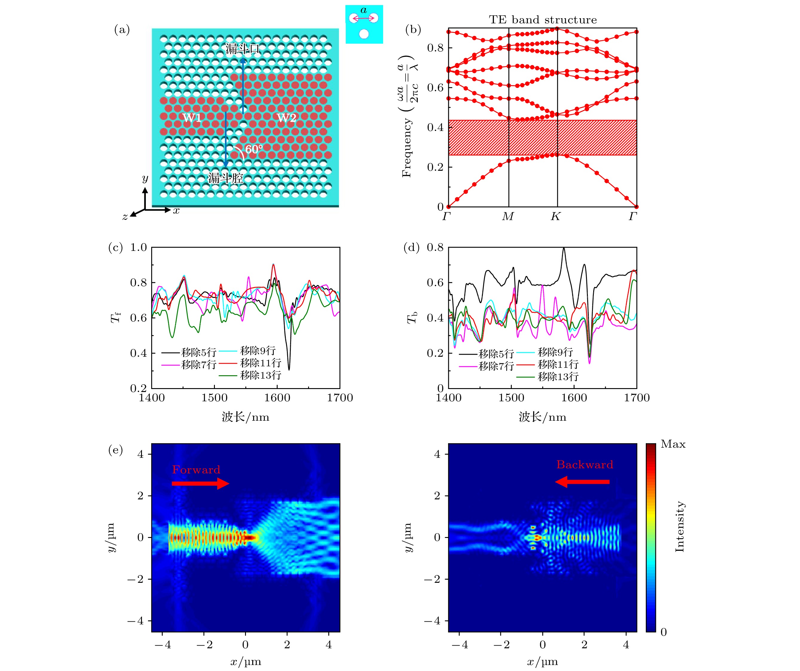
图 1 漏斗型光波导及其传输特性 (a) 漏斗型光波导结构, a = 470 nm为晶格常数, 标为红色的空气孔为线缺陷位置, 移除红色空气孔后形成漏斗型光波导; (b) 光子晶体TE模能带结构图, 其中红色阴影部分为完全禁带部分; W2宽度变化时的正向光波(c)与反向光波(d)传输透射谱, W2宽度分别取移除5行、7行、9行、11行和13行空气孔; (e)正反向光波入射时漏斗型光波导在1550 nm处的场强分布
Fig. 1. Funnel waveguide and transmission characteristics. (a) The structure of funnel waveguide. a = 470 nm is the lattice constant. The air hole marked red is the location of line defect. Remove the red air hole to form a funnel-shaped waveguide. (b) The band structure of the PC. The red shaded area represents the fully photonic bandgap. The transmittance spectra of light waves forward (c) and backward (d) transmit with W2 width-varying. For varying the width of W2, air holes in rows 5, 7, 9, 11 and 13 are removed respectively. (e) The electric field intensity distribution diagrams at 1550 nm in funnel-shaped waveguide.
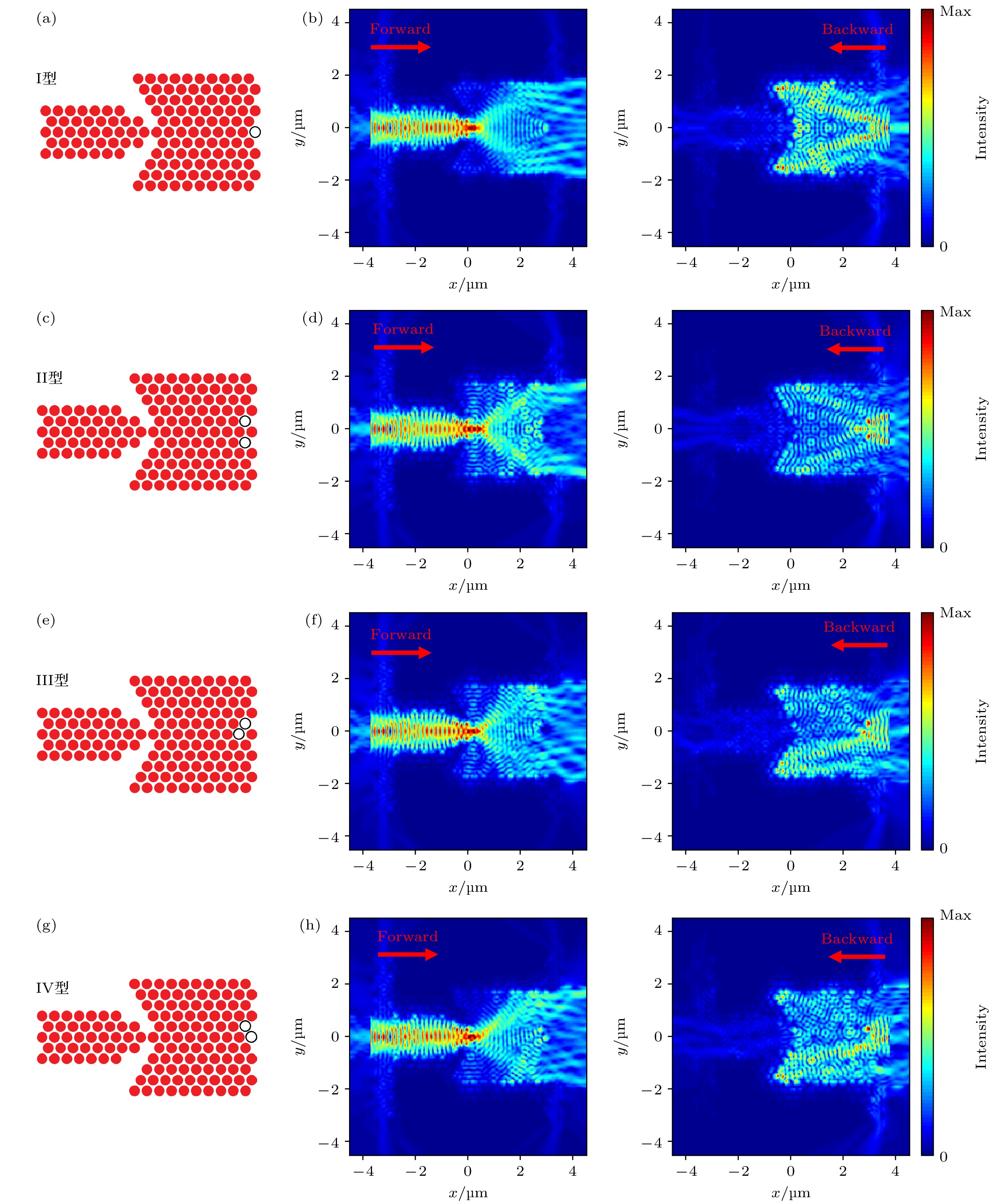
图 2 点缺陷类型及初始位置与场强图, I型(a)、II型(c)、III型(e)和IV型(g)点缺陷及初始位置. 红色圆形表示拟移除空气孔, 白色圆形表示保留的空气孔所形成的点缺陷; 漏斗型光波导中引入I型(b)、II型(d)、III型(f)和IV型(h)点缺陷后正反向光波入射时在1550 nm处的场强分布
Fig. 2. Type and initial position of point defects and the electric field intensity distribution diagrams: The diagrams of type I (a), type II (c), type III (e), type IV (g) of point defects with initial location. The red circle represents the air holes to be removed, and the white circle represents the point defect formed by the retained air holes. The electric field intensity distribution diagrams at 1550 nm in funnel-shaped waveguide with a type I (b), type II (d), type III (f), type IV (h) point defect.
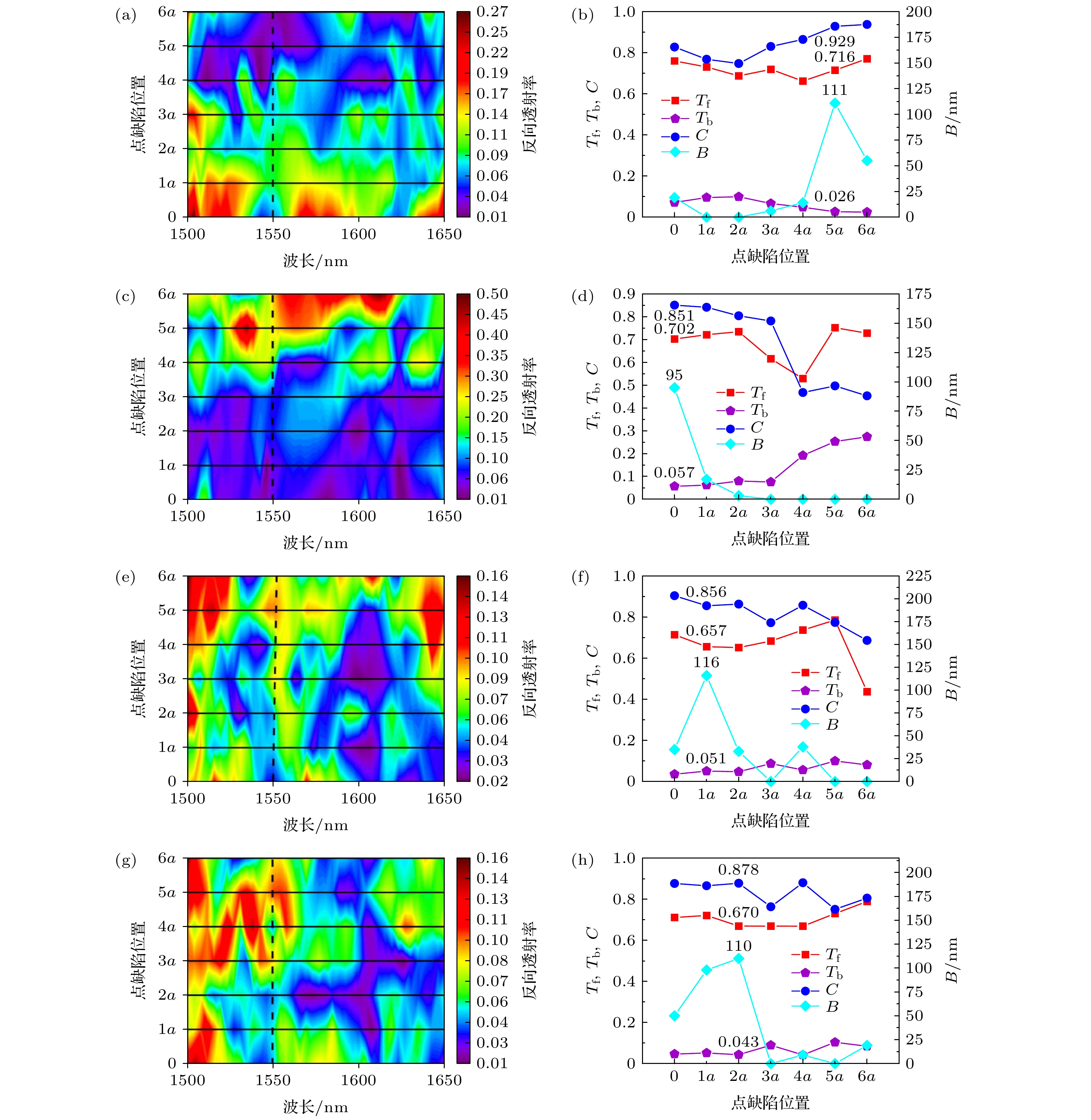
图 3 I型(a)、II型(c)、III型(e)和IV (g)型点缺陷位置移动时的反向光波入射透射谱, 虚线与实线交汇处为点缺陷移动至各位置在1550 nm处的反向透射率值; I型(b)、II型(d)、III型(f)和IV (h)型点缺陷移动至各位置在1550 nm处的Tf (红色线)、Tb (紫色线)、C (蓝色线)和B (青色线)点线图
Fig. 3. Transmittance spectra of light waves backward transmit with type I (a), type II (c), type III (e), type IV (g) defect position movement. The intersection of the dotted line and the solid line is the backward transmittance value at 1550 nm with the point defect movement. The point plot of Tf (red line), Tb (purple line), C (cyan line) and B (orange line) at 1550 nm with type I (b), type II (d), type III (f), type IV (h) point defect position movement.
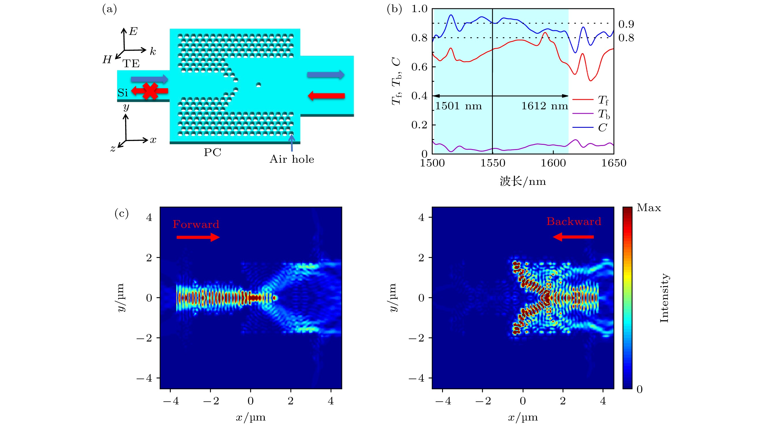
图 4 结构与性能 (a) 本文设计的可实现单向传输的结构示意图, W2宽度为移除11行空气孔, 点缺陷为保留I型第六个空气孔; (b) 单向传输器件透射光谱图(红色线为Tf、紫色线为Tb、蓝色线为C ); (c) TE偏振的正反向入射光在1550 nm处的电场强度分布
Fig. 4. Structure and performance. (a) Schematic drawing of funnel-shaped wave-guide of the realizable unidirectional transmission in this paper. The width of W2 is gained after removing 11 rows of air holes, and the point defect is to retain the sixth air hole of Type I. (b) The transmittance spectra of the unidirectional transmission device (The red line is Tf, the purple line is Tb, and the blue line is C ). (c) The electric field intensity distribution diagrams of forward incident light and backward incident light of TE polarization at the wavelength of 1550 nm.
表 1 在1550 nm处四种类型点缺陷最优位置单向传输性能
Table 1. Optimal location unidirectional transmission performance of four types of point defects at 1550 nm.
点缺陷类型 Tf Tb C B/nm I型, d = 5a 0.716 0.026 0.929 111 II型, d = 0 0.702 0.057 0.851 95 III型, d = 1a 0.657 0.051 0.856 116 IV型, d = 2a 0.670 0.043 0.878 110  下载: 导出CSV
-
[1] Li M 2012 Sci. China Phys. Mech. 55 2316
Google Scholar
[2] Lars T, Qiu M, Srinivasan A 2004 Chem. Phys. Chem. 5 1268
Google Scholar
[3] 武敏, 费宏明, 林瀚, 赵晓丹, 杨毅彪, 陈智辉 2021 物理学报 70 028501
Google Scholar
Wu M, Fei H M, Lin H, Zhao X D, Yang Y B, Chen Z H 2021 Acta Phys. Sin. 70 028501
Google Scholar
[4] Bulgakov E N, Sadreev A F 2014 Opt. Lett. 39 1787
Google Scholar
[5] Soltani A, Ouerghi F, AbdelMalek F 2017 Opt. Commun. 392 147
Google Scholar
[6] Li J, Ye H, Yu Z Y, Liu Y M 2017 Opt. Express 25 19129
Google Scholar
[7] Liu D Y, Yao L F, Zhai X M, Li M H, Dong J F 2014 Appl. Phys. A 116 9
Google Scholar
[8] Ahmet O, Hasan K, Hamza K 2018 J. Opt. Soc. Am. B 35 2111
[9] Ahmet O, Nazmi Y, Hasan K, Hamza K 2019 J. Opt. 21 055104
Google Scholar
[10] Li S, Huang L R, Ling Y H, Liu W B, Ba C F, Li H H 2019 Sci. Rep. 9 17117
Google Scholar
[11] Liu H, Zhang Y Z, Chen C, Bai B B, Zhang X, Zhang H C, Shao Q Y, Wu B, Zhao B L 2021 Opt. Laser Technol. 140 107033
Google Scholar
[12] Hadi R, Mohammad S, Yousef S K 2018 J. Opt. Commun. 39 375
Google Scholar
[13] Wang C, Zhou C Z, Li Z Y 2011 Opt. Express 19 26948
Google Scholar
[14] 刘丹, 胡森 2019 物理学报 024206
Google Scholar
Liu D, Hu S 2019 Acta Phys. Sin. 024206
Google Scholar
[15] Xie J Y, Hu X Y, Wang F F, Ao Y T, Gao W, Yang H, Gong Q H 2018 J. Opt. 20 034004
Google Scholar
[16] Liu B, Liu Y F, Li S J, He X D 2016 Opt. Commun. 368 7
Google Scholar
[17] Liu B, Liu Y F, Jia C, He X D 2016 Aip. Adv. 6 065316
Google Scholar
[18] Ye H, Zhang J Q N, Yu Z Y, Wang D L, Chen Z H 2015 Chin. Phys. B 24 094214
Google Scholar
[19] Ye H, Wang D L, Yu Z Y, Zhang J Q N, Chen Z H 2015 Opt. Express 23 9673
Google Scholar
[20] Chen J J, Huo S Y 2017 Opt. Mater. Express 7 1716
Google Scholar
[21] Fei H M, Zhang Q, Wu M, Lin H, Liu X, Yang Y B, Zhang M D, Guo R, Han X T 2020 Appl. Optics 59 4416
Google Scholar
[22] 费宏明, 严帅, 徐瑜成, 林瀚, 武敏, 杨毅彪, 陈智辉, 田媛, 张娅敏 2020 物理学报 69 184214
Google Scholar
Fei H M, Yan S, Xu Y C, Lin H, Wu M, Yang Y B, Chen Z H, Tian Y, Zhang Y M 2020 Acta Phys. Sin. 69 184214
Google Scholar
[23] Fei H M, Wu M, Lin H, Liu X, Yang Y B, Zhang M D, Cao B Z 2019 Superlatt. Microstruct. 132 106155
Google Scholar
[24] 费宏明, 徐婷, 刘欣, 林瀚, 陈智辉, 杨毅彪, 张明达, 曹斌照, 梁九卿 2017 物理学报 66 204103
Google Scholar
Fei H M, Xu T, Liu X, Lin H, Chen Z H, Yang Y B, Zhang M D, Cao B Z, Liang J Q 2017 Acta Phys. Sin. 66 204103
Google Scholar
[25] Fei H M, Wu M, Lin H, Yang Y B, Liu X, Zhang M D, Cao B Z 2020 Photonic Nanostruct 41 100829
Google Scholar
[26] Fei H M, Yan S, Lin H, Liu X, Yang Y B, Zhang M D, Cao B Z 2020 Opt. Commun. 477 126346
Google Scholar
[27] Fei H M, Wu M, Xu T, Lin H, Yang Y B, Liu X, Zhang M D, Cao B Z 2018 J. Opt. 20 095004
Google Scholar
[28] Ye H, Yu Z Y, Liu Y M, Chen Z H 2016 Opt. Express 24 24592
Google Scholar
[29] Dai D, Wang J, He S 2013 Prog. Electromagn Res. 143 773
Google Scholar
[30] Li C, Liu D, Dai D 2018 Nanophotonics 8 227
Google Scholar


 下载:
下载:
计量
- 文章访问数: 8641
- PDF下载量: 118
- 被引次数: 0
