-
前置电流放大器是扫描隧道显微镜的重要部件之一, 其性能对于扫描隧道显微镜系统的基本操作及新功能开发至关重要. 本文详细分析了影响前置电流放大器性能的因素, 通过筛选噪声极低的运放芯片和电路结构优化, 设计了一款针对扫描隧道显微镜系统的前置电流放大器. 该放大器最灵敏档位(1 GΩ)的噪声低至4
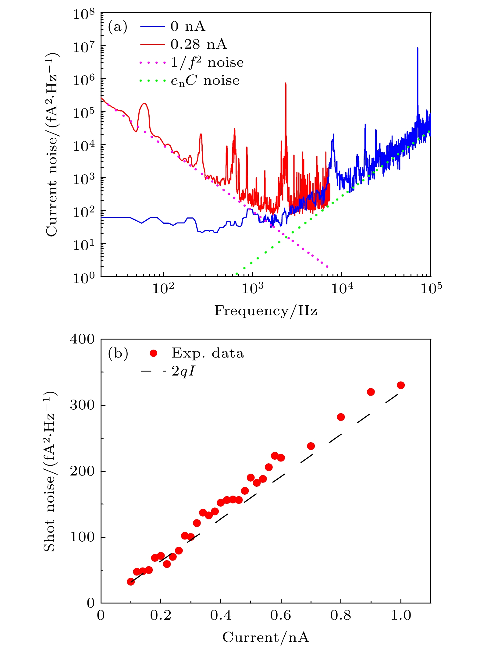
$ {\mathrm{f}}{\mathrm{A}}/\sqrt{{\mathrm{H}}{\mathrm{z}}} $ , 带宽为2.3 kHz, 具有10 MΩ, 100 MΩ和1 GΩ三个测量量程并且可以通过控制信号实现自动切换, 测量范围覆盖pA—μA量级的隧穿电流. 利用该前置电流放大器展示了扫描隧道显微镜系统的主要功能, 包括表面形貌表征、扫描隧道谱测量以及原子搬运, 并探索了隧穿电流中散粒噪声的测量. 通过散粒噪声随隧穿电流的变化关系, 得到隧穿结中散粒噪声的法诺因子约等于1, 验证了简单金属隧穿结中电子隧穿满足泊松过程, 为表面电子关联体系的高精度表征提供了基础.The current preamplifier is one of the important components of the scanning tunneling microscope (STM), and its performance is crucial to the basic operations of the STM system, as well as for the development of demanding novel functionalities such as autonomous atomic fabrication. In this study, the factors that affect the performance of a current preamplifier, including its noise spectrum density and the bandwidth, are analyzed in depth, and a preamplifier is designed and fabricated specifically for the STM system. By using a carefully selected low-noise op amp chip, the optimized current preamplifier has a noise floor as low as 4$ {\mathrm{f}}{\mathrm{A}}/\sqrt{{\mathrm{H}}{\mathrm{z}}} $ and a bandwidth of 2.3 kHz, at its most sensitive transimpedance gain of 1 GΩ. It has three transimpedance gains, 10 MΩ, 100 MΩ, and 1 GΩ, that can be switched through digital control signals. A two-switch configuration is adopted to minimize the noise floor while maintaining the optimal bandwidth. The current detectable by this three-level preamplifier ranges from pA to μA, satisfying the requirements of most STM operations. Using this preamplifier, the fundamental functions of the STM system are successfully demonstrated, including surface topographic characterization, scanning tunneling spectroscopy, and single atom/molecule manipulation. The measurement of shot noise in tunneling current is also explored, and a linear relationship between shot noise and tunneling current is obtained by carefully analyzing noise. It is illustrated that the Fano factor of the shot noise in a normal metallic tunneling junction is approximately equal to 1, revealing the expected Poisson process for electron tunneling in such a scenario. The results are valuable for the high-resolution characterization of correlation systems in the future.-
Keywords:
- scanning tunneling microscope /
- preamplifier /
- shot noise
[1] Binnig G, Rohrer H, Gerber C, Weibel E 1982 Phys. Rev. Lett. 49 57
 Google Scholar
[2] Stroscio J A, Feenstra R M, Fein A P 1986 Phys. Rev. Lett. 57 2579
 Google Scholar
[3] Chen C J 2021 Introduction to Scanning Tunneling Microscopy Third Edition (Vol. 69) (USA: Oxford University Press
[4] Scheiber P, Riss A, Schmid M, Varga P, Diebold U 2010 Phys. Rev. Lett. 105 216101
 Google Scholar
[5] Eigler D M, Schweizer E K 1990 Nature 344 524
 Google Scholar
[6] Bartels L, Meyer G, Rieder K H 1997 Phys. Rev. Lett. 79 697
 Google Scholar
[7] Kalff F E, Rebergen M P, Fahrenfort E, Girovsky J, Toskovic R, Lado J L, Fernandez-Rossier J, Otte A F 2016 Nat. Nanotechnol. 11 926
 Google Scholar
[8] Štubian M, Bobek J, Setvin M, Diebold U, Schmid M 2020 Rev. Sci. Instrum. 91 074701
 Google Scholar
[9] de-Picciotto R, Reznikov M, Heiblum M, Umansky V, Bunin G, Mahalu D 1997 Nature 389 162
 Google Scholar
[10] Saminadayar L, Glattli D C, Jin Y, Etienne B 1997 Phys. Rev. Lett. 79 2526
 Google Scholar
[11] Jehl X, Sanquer M, Calemczuk R, Mailly D 2000 Nature 405 50
 Google Scholar
[12] Bastiaans K M, Chatzopoulos D, Ge J F, Cho D, Tromp W O, van Ruitenbeek J M, Fischer M H, de Visser P J, Thoen D J, Driessen E F C, Klapwijk T M, Allan M P 2021 Science 374 608
 Google Scholar
[13] Kumar A, Saminadayar L, Glattli D C, Jin Y, Etienne B 1996 Phys. Rev. Lett. 76 2778
 Google Scholar
[14] DiCarlo L, Zhang Y, McClure D T, Reilly D J, Marcus C M, Pfeiffer L N, West K W 2006 Phys. Rev. Lett. 97 036810
 Google Scholar
[15] Hashisaka M, Ota T, Yamagishi M, Fujisawa T, Muraki K 2014 Rev. Sci. Instrum. 85 054704
 Google Scholar
[16] Henny M, Oberholzer S, Strunk C, Schönenberger C 1999 Phys. Rev. B 59 2871
 Google Scholar
[17] Chen R, Wheeler P J, Natelson D 2012 Phys. Rev. B 85 235455
 Google Scholar
[18] Bastiaans K M, Benschop T, Chatzopoulos D, Cho D, Dong Q, Jin Y, Allan M P 2018 Rev. Sci. Instrum. 89 093709
 Google Scholar
[19] Kay A 2012 Operational Amplifier Noise: Techniques and Tips for Analyzing and Reducing Noise (Elsevier) pp13–14
[20] Horowitz P, Hill W, Robinson I 1989 The art of electronics (Vol. 2) (Cambridge: Cambridge university Press) pp171–184
[21] Mikhael W B, Michael S 1987 IEEE T. Circuits Syst. 34 449
 Google Scholar
[22] Blanter Y M, Büttiker M 2000 Physics Reports 336 1
 Google Scholar
[23] Kobayashi K, Hashisaka M 2021 J Phys Soc Jpn 90 102001
 Google Scholar
[24] Birk H, De Jong M, Schönenberger C 1995 Phys. Rev. Lett. 75 1610
 Google Scholar
-
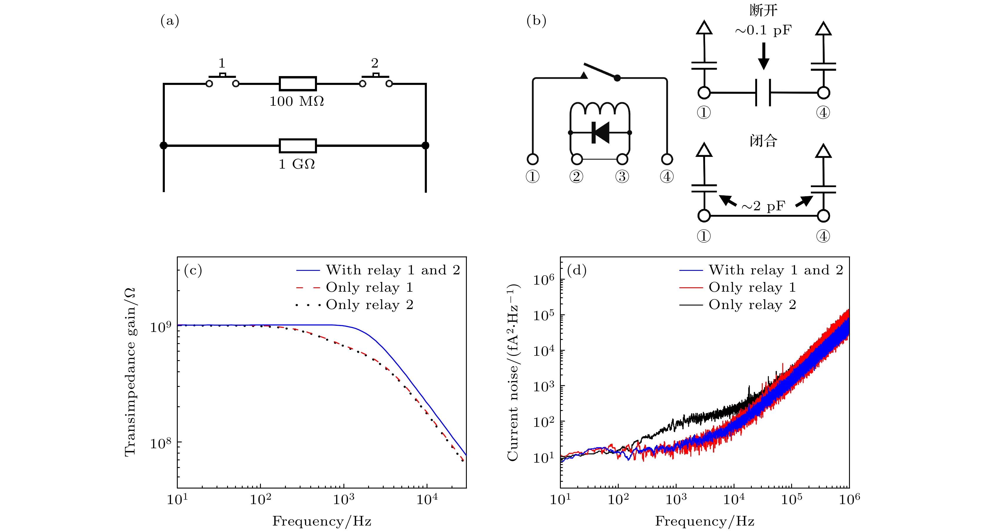
图 3 (a)多量程开关控制设计; (b)继电器结构示意图及其电容特征; (c), (d) 3种不同开关状态下1 GΩ档的增益和等效电流噪声谱密度
Fig. 3. (a) Switching circuit for multiple gain control; (b) schematic diagram of electromagnetic relay and related typical capacitances; (c), (d) the gain and input current noise spectrum density with 1 GΩ transimpedance gain under three different switch conditions.
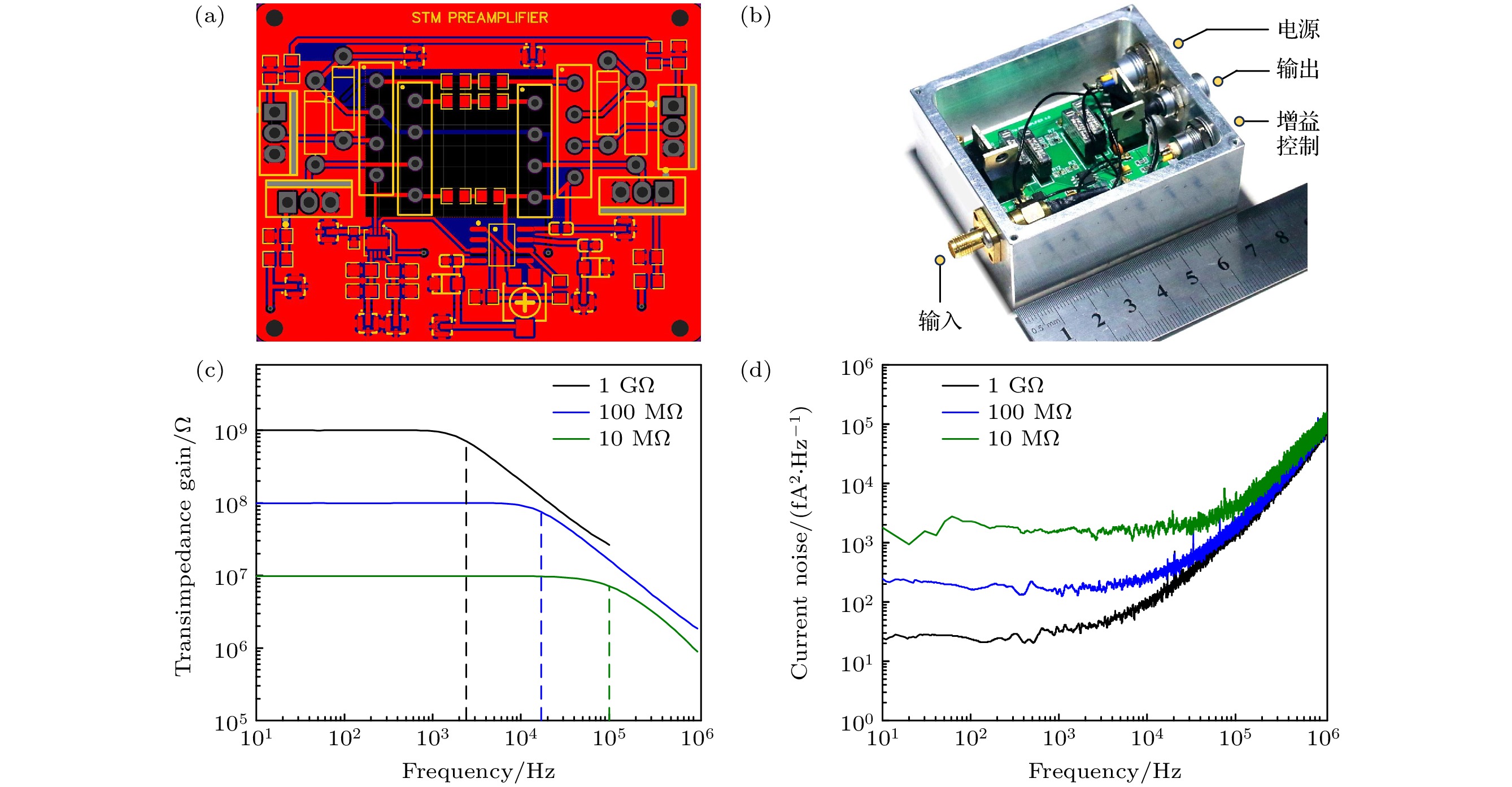
图 4 (a)前置电流放大器PCB设计图; (b)前置电流放大器实物图; (c)不同反馈电阻对应的跨阻增益曲线; (d)不同反馈电阻对应的等效输入电流噪声谱密度
Fig. 4. (a) PCB layout of the preamplifier circuit; (b) photo of the current preamplifier; (c) measured transimpedance gain with different feedback resistors; (d) equivalent input current spectrum density of three gains.
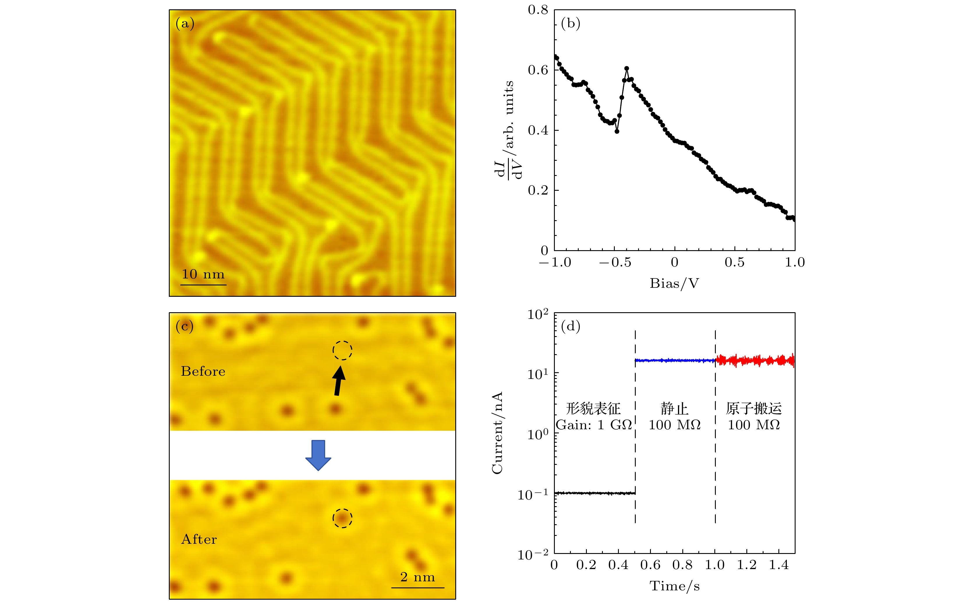
图 5 (a) 78 K温度下Au(111)表面的STM形貌表征(V = 0.5 V, I = 0.3 nA); (b) 隧穿电流微分电导谱; (c) 7 K温度条件下原子搬运前后形貌图(V = 0.2 V, I = 1 nA); (d)不同操作功能下的隧穿电流曲线
Fig. 5. (a) STM topographic image (V = 0.5 V, I = 0.3 nA) of Au(111) surface at 78 K; (b) tunneling differential conductance spectrum measured on Cu(111) surface; (c) STM topographs (V = 0.2 V, I = 1 nA) before and after atomic manipulation at 7 K; (d) tunneling current under different STM operations.
表 1 自制前置电流放大器与三款商业化产品的主要参数对比
Table 1. Main parameters of home-built preamplifier and three commercial products.
Gain/(V·A–1) Input noise
@109 V/A/(fA·Hz–1/2)–3 dB bandwidth
@109 V/AGain control
(manual, remote)自研放大器 $ {10}^{7}—{10}^{9} $ 4.0 2.3 kHz R 商用放大器A $ {10}^{3}—{10}^{11} $ 4.3 1.1 kHz M, R 商用放大器B $ {10}^{3}—{10}^{11} $ 5.0 1.0 kHz M 商用放大器C $ {10}^{3}—{10}^{12} $ 10.0 15.0 Hz M, R -
[1] Binnig G, Rohrer H, Gerber C, Weibel E 1982 Phys. Rev. Lett. 49 57
 Google Scholar
[2] Stroscio J A, Feenstra R M, Fein A P 1986 Phys. Rev. Lett. 57 2579
 Google Scholar
[3] Chen C J 2021 Introduction to Scanning Tunneling Microscopy Third Edition (Vol. 69) (USA: Oxford University Press
[4] Scheiber P, Riss A, Schmid M, Varga P, Diebold U 2010 Phys. Rev. Lett. 105 216101
 Google Scholar
[5] Eigler D M, Schweizer E K 1990 Nature 344 524
 Google Scholar
[6] Bartels L, Meyer G, Rieder K H 1997 Phys. Rev. Lett. 79 697
 Google Scholar
[7] Kalff F E, Rebergen M P, Fahrenfort E, Girovsky J, Toskovic R, Lado J L, Fernandez-Rossier J, Otte A F 2016 Nat. Nanotechnol. 11 926
 Google Scholar
[8] Štubian M, Bobek J, Setvin M, Diebold U, Schmid M 2020 Rev. Sci. Instrum. 91 074701
 Google Scholar
[9] de-Picciotto R, Reznikov M, Heiblum M, Umansky V, Bunin G, Mahalu D 1997 Nature 389 162
 Google Scholar
[10] Saminadayar L, Glattli D C, Jin Y, Etienne B 1997 Phys. Rev. Lett. 79 2526
 Google Scholar
[11] Jehl X, Sanquer M, Calemczuk R, Mailly D 2000 Nature 405 50
 Google Scholar
[12] Bastiaans K M, Chatzopoulos D, Ge J F, Cho D, Tromp W O, van Ruitenbeek J M, Fischer M H, de Visser P J, Thoen D J, Driessen E F C, Klapwijk T M, Allan M P 2021 Science 374 608
 Google Scholar
[13] Kumar A, Saminadayar L, Glattli D C, Jin Y, Etienne B 1996 Phys. Rev. Lett. 76 2778
 Google Scholar
[14] DiCarlo L, Zhang Y, McClure D T, Reilly D J, Marcus C M, Pfeiffer L N, West K W 2006 Phys. Rev. Lett. 97 036810
 Google Scholar
[15] Hashisaka M, Ota T, Yamagishi M, Fujisawa T, Muraki K 2014 Rev. Sci. Instrum. 85 054704
 Google Scholar
[16] Henny M, Oberholzer S, Strunk C, Schönenberger C 1999 Phys. Rev. B 59 2871
 Google Scholar
[17] Chen R, Wheeler P J, Natelson D 2012 Phys. Rev. B 85 235455
 Google Scholar
[18] Bastiaans K M, Benschop T, Chatzopoulos D, Cho D, Dong Q, Jin Y, Allan M P 2018 Rev. Sci. Instrum. 89 093709
 Google Scholar
[19] Kay A 2012 Operational Amplifier Noise: Techniques and Tips for Analyzing and Reducing Noise (Elsevier) pp13–14
[20] Horowitz P, Hill W, Robinson I 1989 The art of electronics (Vol. 2) (Cambridge: Cambridge university Press) pp171–184
[21] Mikhael W B, Michael S 1987 IEEE T. Circuits Syst. 34 449
 Google Scholar
[22] Blanter Y M, Büttiker M 2000 Physics Reports 336 1
 Google Scholar
[23] Kobayashi K, Hashisaka M 2021 J Phys Soc Jpn 90 102001
 Google Scholar
[24] Birk H, De Jong M, Schönenberger C 1995 Phys. Rev. Lett. 75 1610
 Google Scholar
计量
- 文章访问数: 5869
- PDF下载量: 226
- 被引次数: 0


 下载:
下载:
